Language selection

Search

Patent 2022251 Summary

Third-party information liability

Some of the information on this Web page has been provided by external sources. The Government of Canada is not responsible for the accuracy, reliability or currency of the information supplied by external sources. Users wishing to rely upon this information should consult directly with the source of the information. Content provided by external sources is not subject to official languages, privacy and accessibility requirements.

Claims and Abstract availability

Any discrepancies in the text and image of the Claims and Abstract are due to differing posting times. Text of the Claims and Abstract are posted:

  • At the time the application is open to public inspection;
  • At the time of issue of the patent (grant).
(12) Patent: (11) CA 2022251
(54) English Title: ELECTRON-DETECTOR DIODE BIASSING SCHEME FOR IMPROVED WRITING BY AN ELECTRON BEAM LITHOGRAPHY MACHINE
(54) French Title: METHODE DE POLARISATION DE DIODES DE DETECTION D'ELECTRONS AMELIORANT L'ECRITURE DANS UNE MACHINE LITHOGRAPHIQUE A FAISCEAU ELECTRONIQUE
Status: Expired and beyond the Period of Reversal
Bibliographic Data
(51) International Patent Classification (IPC):
  • H01L 21/42 (2006.01)
  • H01J 37/244 (2006.01)
  • H01J 37/317 (2006.01)
(72) Inventors :
  • DEVORE, WILLIAM JAY (United States of America)
(73) Owners :
  • ETEC SYSTEMS, INC.
(71) Applicants :
  • ETEC SYSTEMS, INC. (United States of America)
(74) Agent: OSLER, HOSKIN & HARCOURT LLP
(74) Associate agent:
(45) Issued: 1998-07-07
(22) Filed Date: 1990-07-30
(41) Open to Public Inspection: 1991-02-09
Examination requested: 1994-10-27
Availability of licence: N/A
Dedicated to the Public: N/A
(25) Language of filing: English

Patent Cooperation Treaty (PCT): No

(30) Application Priority Data:
Application No. Country/Territory Date
391,202 (United States of America) 1989-08-08

Abstracts

English Abstract


Disclosed is a biassing scheme for a beam position
location apparatus (50) which comprises electron detector
diodes (52) in an electron beam lithography machine (10)
such that the detector diodes (52) deposit fewer
secondary electrons (62) on a substrate (16) being
processed by the electron beam (22) and thus reduce or
eliminate any charge buildup on said substrate which
deflect the electron beam (22) causing pattern
distortion.


French Abstract

L'invention est une méthode de polarisation pour un dispositif de positionnement de faisceaux (50) pour machine de lithographique à faisceau électronique (10) qui comprend des diodes de détection d'électrons (52) qui déposent moins d'électrons secondaires (62) sur le substrat (16) traité par le faisceau électronique (22), ce qui réduit ou élimine les charges d'électricité statique sur ce substrat qui produisent des distorsions en faisant dévier le faisceau électronique (22).

Claims

Note: Claims are shown in the official language in which they were submitted.

- 6 -
The embodiments of the invention in which an exclusive
property or privilege is claimed are defined as follows:
1. In an electron beam lithography machine with a beam
column and having a controlled electron beam capable of writing
a pattern on a substrate located beneath the beam column, the
improvement in a beam position locating apparatus comprising
electron detector means which locates the beam position by
responding to backscattered electrons generated by the electron
bombardment from reaching said substrate on said substrate by
said electron beam and means to reduce or eliminate secondary
electrons emitted from said detector in response to said
bombardment thereby reducing or eliminating a charge buildup on
said substrate which would deflect said beam and cause pattern
distortion.
2. The machine as claimed in claim 1 wherein the means to
reduce or eliminate said secondary electrons from reaching said
substrate comprises a biassing means on said electron detector
means to attract said secondary electrons.
3. The machine as claimed in claim 2 wherein said biassing
means comprises the application of a voltage on said detector
means which is positive with respect to said substrate.
4. The machine as claimed in claim 1 wherein said electron
detector means comprises diode means and wherein the means to
reduce or eliminate said secondary electrons comprises a biassing
means on said diode means to attract said secondary electrons
from reaching said substrate.
5. The machine as claimed in claim 4 wherein said biassing
means comprises the application of a voltage on said diode means
which is positive with respect to said substrate.

Description

Note: Descriptions are shown in the official language in which they were submitted.


';'-'J 2~2225~
ET-3888
ELECTRON-DETECTOR DIODE BIASSING SCHEME
FOR IMPROVED WRITING BY
; AN ELECTRON BEAM LITHOGRAPHY MACHINE
oS BACKGROUND OF THE INVENTION
This invention relates, in general, to electron beam
lithography and is particularly directed to the reduction
in pattern distortion during beam writing on a workpiece
in an electron beam lithography machine.
In an electron beam lithography machine, there is a
beam column in which an electron beam is electronically
and magnetically controlled and projected onto a
workpiece which is mounted on a movable stage to perform
a writing operation on the workpiece. The workpiece
15 also called a substrate and may be a resist coated wafer
or a resist coated mask located below the beam column.
When the electron beam bombards the substrate, the
beam produces high energy backscattered electrons which
are reflected upwardly and outwardly from the impact
20 point and which are sensed by electron detector diodes
located near the exit of the beam column to detect the
position of the beam at the point of impact. However,
when these backscattered electrons bombard the electron
detector diodes, these detector diodes themselves emit
25 more backscattered electrons and also secondary electrons
of lesser energy, both of which are directed down onto
.:
.~ ::

': 2~22~1
the substrate because of the close proximity of the
substrate to the detector diodes. The backscattered
electrons are able to penetrate the resist but the
secondary electrons, because of their lesser energy, are
05 deposited on the resist, which is non-conducting, and
cause a charge buildup on the resist which in turn can
deflect the electron beam. This means that the electron
beam may not be bombarding the substrate where it is
supposed to and this leads to pattern distortion.
It is therefore an object of this invention to reduce
or eliminate pattern distortion caused by secondary
electrons emitted by the electron detector diodes used in
an electron beam lithography machine.
SUMMARY OF THE INVENTION
The invention which attains the foregoing object
comprises a biassing scheme for electron detector diodes
in an electron beam lithography system such that ~he
detector diodes deposit fewer secondary electrons on a
20 substrate during writing by the electron beam and thus
reduce or eliminate the charge buildup caused by the
secondary electrons on the substrate which deflects the
beam position resulting in pattern distortion.
25 BRIEF DESCRIPTION OF THE DRAWINGS
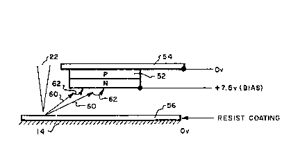
Figure 1 is a schematic illustration of an electron
beam lithography machine incorporating electron
detectors,
Figure 2 is a bottom view of the electron beam column
30 showing the electron detector arrangement near the exit
of the electron beam,
Figure 3 is a schematic illustration of one prior art
electron detector and illustrating the secondary
electrons being deposited on the substrate surface which
35 cause pattern distortion,
Figure 4 is a schematic illustration of one electron

; 20222~
detector of this invention and illustrating an absence of
the secondary electrons being deposited on the substrate
which would have otherwise caused pattern distortion, and
Figures 5 and 6 illustrate a comparison of the test
05 patterns showing the pattern distortion caused by the
prior art electron detector and the writing improvement
as a result of this invention.
DETAILED DESCRIPTION
In the schematic illustration, figure 1, the electron
beam lithography machine incorporating this invention is
identified in its entirety as 10. The machine includes
an electron beam column 12 and a workholding apparatus 14
upon which a workpiece 16 is loaded, processed and
unloaded. The workpiece 16 is a semiconductor wafer or --
mask and is referred to as a substrate or simply a wafer.
As part of the beam column 12, there is provided an
electron beam source 20, demagnification, projection and
deflection optics which generate a finely focused beam 22
20 and may also include illumination and shaping optics when
a shaped beam is used. A central tube 24, (shown in
phantom) within the column 12 is traversed by the beam 22
and maintained at a high vacuum by a high vacuum pump 26
coupled to the column 12. The beam 22 passes through an
aperture 28 in the column and impinges on the substrate
16 for processing the latter. The complete lithography
machine further includes a computer (controller) and
associated binary electronics which controls the beam 22,
controls a drive system ~or driving the workholding
30 apparatus 14, stores pattern data and provides beam
control signals; all identified by a block dia8ram 30.
In the simplified schematic illustration of figure 1,
the workholding apparatus 14 includes a stage 32 which is
driven in the x-y direction and in the z direction by
35 conventional drives and its position sensed by a sensing
system; all identified by block diagram 34. As further
- ~:

~0.~.?~
--4--
shown in figure 1, the electron beam lithography machine
10 also includes a electron beam detection apparatus 50
in the form of a plurality of electron detector diodes 52
mounted on a plate 54 and positioned in close proximity
05 to the aperture 28. Figure 2 shows four such diodes
A,B,C and D, connected to conductor 53, surrounding the
aperture 28.
In the schematic enlargement of one detector diode
52, figure 3, and biased according to the prior art, the
electron beam 22 is shown penetrating a non-conductive
resist coating 56 on the substrate 16. In this
arrangement, the substrate 14 is biased at 0.0 volt, the
detector diode 52 at 0.0 volt and the plate 54 at some
negative potential, such as -7.5 volts. With this bias,
the bombardment of the substrate by the electron beam 22
causes backscattered electrons, represented by arrows 60,
to travel toward the electron detector 52 which, in turn,
emits both backscattered electrons (not shown) and
secondary electrons, represented by arrows 62, directed
toward the resist coating 56. These secondary electrons
62 have lower energy and are thus unable to penetrate the
resist coating 56. This causes a charge buildup on the
resist surface which, in turn, can deflect the beam 22 so
that the beam may not bombard the substrste 16 where it
is supposed to and thus cause pattern distortion.
Figure 4, which is similar to figure 3, but shows the
bias on the detector diode 52 relative to the substrate
16 according to the bias scheme of this invention. This
bias is 0.0 volts on the substrate 16, + 7.5 volts on the
diode 52 and 0.0 volts on the plate 54. This figure also
shows that because of the bias scheme, the secondary
electrons 62 with energy less than 7.5 eV do not travel
to resist 66 and thus do not cause a charge buildup to
affect the placement of the electron beam 22.
Figure 5 shows the effect of pattern distortion
caused by the charge buildup on the substrate and figure
6 shows the correction of the pattern utilizing the

5 ~ ~
present invention.
More specifically, figure 5 shows an underlying grid
70 comprising a plurality of squares with an overlying
pattern 72 of distorted squares. Each of the distorted
o5 squares has a point 74 in its upper left hand corner.
These points 74 represent the location of crosses (not
shown) which were written by a machine under test. These
marks formed an llxll array on a mask 125 mm square with
the spacing between the crosses being 12.5 mm. This mask
10 was processed and then placed in a second machine which
located the crosses at points, such as 74, and determined
the coordinants of each of the crosses. In plotting the
errors, the distance between the undistorted square
corners is the amount shown in HSCALE (horizontal) or
15 VSCALE (vertical). In figure 5, the crescent-shaped
distortion 76 in the upper right hand corner shows errors
of about 0.1 micrometer (um). This crescent 76 is caused
by the secondary electrons from the diode detector 52 in
the following way. During the period of beam adjustment,
20 lasting about five minutes, preceeding pattern writing,
the beam 22 is positioned at a test target approximately
15 mm off the writing surface just above the crescent
76. It is during this five minute period that secondary
electrons accumulate on the writing surface just above
(as shown in the drawings) where the top row of crosses
will be written. The charge remains long enough to
deflect the first row of crosses and produce the
characteristic crescent distortion 76.
Figure 6 is written with this invention in place.
30 Note that the HSCALE/VSCALE numbers have changed to 0.100
um because of smaller errors being found. There is no
trace of the crescent distortion 76.

Representative Drawing
A single figure which represents the drawing illustrating the invention.
Administrative Status

2024-08-01:As part of the Next Generation Patents (NGP) transition, the Canadian Patents Database (CPD) now contains a more detailed Event History, which replicates the Event Log of our new back-office solution.

Please note that "Inactive:" events refers to events no longer in use in our new back-office solution.

For a clearer understanding of the status of the application/patent presented on this page, the site Disclaimer , as well as the definitions for Patent , Event History , Maintenance Fee  and Payment History  should be consulted.

Event History

Description Date
Inactive: IPC from MCD 2006-03-11
Time Limit for Reversal Expired 2003-07-30
Letter Sent 2002-07-30
Grant by Issuance 1998-07-07
Letter Sent 1998-04-14
Amendment After Allowance Requirements Determined Compliant 1998-04-14
Amendment After Allowance (AAA) Received 1998-02-27
Pre-grant 1998-02-27
Inactive: Amendment after Allowance Fee Processed 1998-02-27
Inactive: Final fee received 1998-02-27
Notice of Allowance is Issued 1998-01-02
Letter Sent 1998-01-02
Inactive: Status info is complete as of Log entry date 1997-12-29
Inactive: Application prosecuted on TS as of Log entry date 1997-12-29
Inactive: First IPC assigned 1997-12-12
Inactive: IPC assigned 1997-12-12
Inactive: Approved for allowance (AFA) 1997-12-12
Inactive: Delete abandonment 1997-12-12
Inactive: IPC removed 1997-12-12
Inactive: Abandon-RFE+Late fee unpaid-Correspondence sent 1997-07-30
All Requirements for Examination Determined Compliant 1994-10-27
Request for Examination Requirements Determined Compliant 1994-10-27
Application Published (Open to Public Inspection) 1991-02-09

Abandonment History

There is no abandonment history.

Maintenance Fee

The last payment was received on 1997-07-28

Note : If the full payment has not been received on or before the date indicated, a further fee may be required which may be one of the following

  • the reinstatement fee;
  • the late payment fee; or
  • additional fee to reverse deemed expiry.

Please refer to the CIPO Patent Fees web page to see all current fee amounts.

Fee History

Fee Type Anniversary Year Due Date Paid Date
Request for examination - standard 1994-10-27
MF (application, 7th anniv.) - standard 07 1997-07-30 1997-07-28
Final fee - standard 1998-02-27
1998-02-27
MF (patent, 8th anniv.) - standard 1998-07-30 1998-07-21
MF (patent, 9th anniv.) - standard 1999-07-30 1999-06-30
MF (patent, 10th anniv.) - standard 2000-07-31 2000-07-04
MF (patent, 11th anniv.) - standard 2001-07-30 2001-07-05
Owners on Record

Note: Records showing the ownership history in alphabetical order.

Current Owners on Record
ETEC SYSTEMS, INC.
Past Owners on Record
WILLIAM JAY DEVORE
Past Owners that do not appear in the "Owners on Record" listing will appear in other documentation within the application.
Documents

To view selected files, please enter reCAPTCHA code :


To view images, click a link in the Document Description column. To download the documents, select one or more checkboxes in the first column and then click the "Download Selected in PDF format (Zip Archive)" or the "Download Selected as Single PDF" button.

List of published and non-published patent-specific documents on the CPD .

If you have any difficulty accessing content, you can call the Client Service Centre at 1-866-997-1936 or send them an e-mail at CIPO Client Service Centre.


Document
Description 
Date
(yyyy-mm-dd) 
Number of pages   Size of Image (KB) 
Cover Page 1994-02-26 1 13
Drawings 1994-02-26 3 74
Abstract 1994-02-26 1 10
Claims 1994-02-26 1 31
Description 1994-02-26 5 162
Claims 1998-02-27 1 42
Cover Page 1998-07-06 1 40
Representative drawing 1998-07-06 1 6
Commissioner's Notice - Application Found Allowable 1998-01-02 1 165
Maintenance Fee Notice 2002-08-27 1 177
Fees 1999-06-30 1 35
Correspondence 1998-02-27 2 50
Correspondence 1998-04-14 1 8
Correspondence 1998-04-29 1 49
Correspondence 1998-04-29 1 13
Fees 2001-07-05 1 42
Fees 1997-07-28 1 42
Fees 1998-07-21 1 43
Fees 1996-07-29 1 37
Fees 1995-06-30 1 30
Fees 1992-06-01 1 20
Fees 1994-06-20 1 37
Fees 1993-05-18 1 21
Fees 1996-05-17 1 32
PCT Correspondence 1992-01-10 1 26
Courtesy - Office Letter 1994-11-21 1 52
Prosecution correspondence 1995-01-03 3 74
Prosecution correspondence 1994-10-27 1 35