Some of the information on this Web page has been provided by external sources. The Government of Canada is not responsible for the accuracy, reliability or currency of the information supplied by external sources. Users wishing to rely upon this information should consult directly with the source of the information. Content provided by external sources is not subject to official languages, privacy and accessibility requirements.
Any discrepancies in the text and image of the Claims and Abstract are due to differing posting times. Text of the Claims and Abstract are posted:
| (12) Patent Application: | (11) CA 2023172 |
|---|---|
| (54) English Title: | METHOD TO MANUFACTURE DOUBLE-POLY CAPACITORS |
| (54) French Title: | METHODE DE FABRICATION DE CONDENSATEURS A DEUX POLYMERES |
| Status: | Deemed Abandoned and Beyond the Period of Reinstatement - Pending Response to Notice of Disregarded Communication |
| (51) International Patent Classification (IPC): |
|
|---|---|
| (72) Inventors : |
|
| (73) Owners : |
|
| (71) Applicants : |
|
| (74) Agent: | MARKS & CLERK |
| (74) Associate agent: | |
| (45) Issued: | |
| (22) Filed Date: | 1990-08-13 |
| (41) Open to Public Inspection: | 1992-02-14 |
| Examination requested: | 1997-05-27 |
| Availability of licence: | N/A |
| Dedicated to the Public: | N/A |
| (25) Language of filing: | English |
| Patent Cooperation Treaty (PCT): | No |
|---|
| (30) Application Priority Data: | None |
|---|
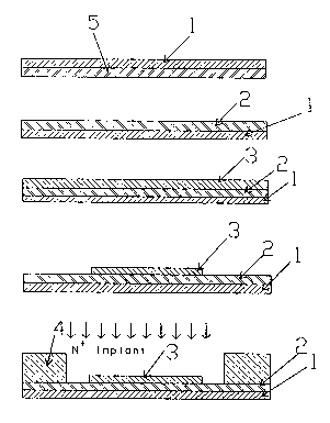
ABSTRACT
A method a manufacturing integrated circuits including
transistors, capacitors, and resistors, comprises the steps
of forming a first poly layer, which is heavily doped;
forming a dielectric layer over the first poly layer; forming
a second poly layer over the dielectric layer, the second
poly layer being lightly doped; and subsequently further
doping the second poly layer at least in capacitor regions
while masking the second poly layer in resistor regions so as
to heavily dope the second poly layer in the capacitor
regions and thereby improve capacitor linearity while
substantially maintaining the resistivity of the lightly
doped second poly layer in the resistor regions. In this way
capacitors having good linearity can be fabricated at the
same time as small area resistors with good contact
resistance.
Note: Claims are shown in the official language in which they were submitted.
Note: Descriptions are shown in the official language in which they were submitted.
2024-08-01:As part of the Next Generation Patents (NGP) transition, the Canadian Patents Database (CPD) now contains a more detailed Event History, which replicates the Event Log of our new back-office solution.
Please note that "Inactive:" events refers to events no longer in use in our new back-office solution.
For a clearer understanding of the status of the application/patent presented on this page, the site Disclaimer , as well as the definitions for Patent , Event History , Maintenance Fee and Payment History should be consulted.
| Description | Date |
|---|---|
| Inactive: IPC from MCD | 2006-03-11 |
| Application Not Reinstated by Deadline | 2001-08-13 |
| Time Limit for Reversal Expired | 2001-08-13 |
| Letter Sent | 2001-06-13 |
| Deemed Abandoned - Conditions for Grant Determined Not Compliant | 2000-11-01 |
| Deemed Abandoned - Failure to Respond to Maintenance Fee Notice | 2000-08-14 |
| Notice of Allowance is Issued | 2000-05-01 |
| Notice of Allowance is Issued | 2000-05-01 |
| Letter Sent | 2000-05-01 |
| Inactive: Approved for allowance (AFA) | 2000-04-14 |
| Inactive: Multiple transfers | 1998-02-16 |
| Inactive: Application prosecuted on TS as of Log entry date | 1997-06-25 |
| Letter Sent | 1997-06-25 |
| Inactive: Status info is complete as of Log entry date | 1997-06-25 |
| Request for Examination Requirements Determined Compliant | 1997-05-27 |
| All Requirements for Examination Determined Compliant | 1997-05-27 |
| Application Published (Open to Public Inspection) | 1992-02-14 |
| Abandonment Date | Reason | Reinstatement Date |
|---|---|---|
| 2000-11-01 | ||
| 2000-08-14 |
The last payment was received on 1999-06-30
Note : If the full payment has not been received on or before the date indicated, a further fee may be required which may be one of the following
Patent fees are adjusted on the 1st of January every year. The amounts above are the current amounts if received by December 31 of the current year.
Please refer to the CIPO
Patent Fees
web page to see all current fee amounts.
| Fee Type | Anniversary Year | Due Date | Paid Date |
|---|---|---|---|
| Request for examination - standard | 1997-05-27 | ||
| MF (application, 7th anniv.) - standard | 07 | 1997-08-13 | 1997-08-13 |
| Registration of a document | 1998-02-16 | ||
| MF (application, 8th anniv.) - standard | 08 | 1998-08-13 | 1998-08-05 |
| MF (application, 9th anniv.) - standard | 09 | 1999-08-13 | 1999-06-30 |
| Registration of a document | 2001-05-04 |
Note: Records showing the ownership history in alphabetical order.
| Current Owners on Record |
|---|
| MITEL CORPORATION |
| Past Owners on Record |
|---|
| FRANCOIS L. CORDEAU |
| GORD HARLING |

