Note: Descriptions are shown in the official language in which they were submitted.
~ 3;~
IMPROVEMENTS IN OR RELATING TO PRINTED CIRCUIT ~OARDS
This invention relates to improvements in or
relating to printed circuit boards.
Conventionally, printed circuit boards are pro-
5 vided with holes for acceptance of circuit board pins andeach circuit board pin communicates with circuitry provided
by the circuit board.
At the present time efforts are being made to
miniaturize electrical and electronic circuitry and its
10 component parts. While many improvements have been made in
this respect, not only with regard to the sizes of solid
state chips for performing multiple electronic function,
efforts to reduce the size of printed circuit hoards have
been somewhat frustrated.
Another problem is related to the provision of
electrical conductors extending from one side to the other
on a board for the purpose of interconnecting together
circuits on the two sides. These conductors are
hereinafter referred to as "through-hole conductors".
20 Holes are drilled in a board, the ho]es then being filled
with copper by deposition techniques to form the through-
hole conductors. These holes which may be spaced apart by
only 0.100 inches, only require to have diameters around
0.013 inches to provide sufficient cross-sectional area for
25 the through-hole conductors for their electrical require-
ments. However, there are various problems ~ssociated with
the provision of the small diameter holes particularly the
problem of drill breakage.
The present invention seeks to provide a circuit
30 board which may carry a high concentration of circuitry
thereby enabling the size of the board to be minimized
while performing its required function. The present in- ;
vention also seeks to provide a method of providing a
circuit board with electrical conductors within holes ~nd
35 which minimizes the above problems.
Accordingly, the present invention provides a
printed circuit board comprising a substrate defining a
plurality of holes and at least two electrical conductors
: ; ' .
.
'~
~?', . ~
are provided upon the surface of each hole, the conductors
being spaced apart from one another circumferentially of
each hole so as to be electrically isolated from one
another, with each conductor electrically connected to an
5 individual circuit line carried by the substrate and ex-
tending towards the hole.
In a circuit board according to the invention,
holes provided with two or more electrical conductors may
be used for receiving circuit board pins, one pin to each
10 hole. In this case, the electrical conductors of these
holes provide electrical terminals for engagement with
electrical conductor lines extending longitudinally of the
pins. These pins, specifically designed for insertion into
their individual holes have a plurality of individual con-
15 ductor lines which are electrically isolated from oneanother. Thus, with this construction, spacing of the
terminals ~or each individual circuit line is not deter-
mined by the spacing of the holes in the board. In con-
trast, the density of the terminal positions is determined
20 by the hole spacing and also by the number of terminals
provided at each hole. Hence, for a given hole spacing,
more terminals are provided in the board for contact with
circuit board pins and a denser board circuitry is made
possible.
Alternatively, two or more electrical conductors
of a hole may be used as through-hole conductors to inter-
connect circuits together on the two sides of the board.
In this case, each hole may be drilled with a substantially
large diameter, e.g. approximately that for receiving a
30 circuit board pin (perhaps in the region of 0.040 inch
diameter), so that the problems associated with drilling
small diameter holes around 0.013 inches are minimized or
overcome. Each through-hole conductor which e~tends
circumferentially for a distance around its hole is ea~ily
35 provided with its required cross-sectional dimensions for
electrical requirements by known plating techniques.
Conveniently, each electrical conductor in a hole
is provided as an arcuate layer which extends partly around
.
: ' ! '
.
'`',` ; ',
':
: ~
the surface of its hole. In the case where the conductors
are to be used as through-hole conductors, then the space
within each hole which is unoccupied by the conductor
material may be at least partly blocked by a plug of di-
5 electric material.
Each electrical conductor within each hole is
preferably comprises an electrolessly deposited underlayer
and a further layer covering the underlayer. Also, each
circuit line, when carried upon one side of the substrate,
10 preferably comprises an underlayer laminated to the
substrate and then second and third layers formed,
respectively, by electroless deposition and electroplating
techniques.
The invention further comprises an assembly of a
15 printed circuit board and a plurality of pins wherein the
circuit board defines a plurality of holes and at least two
electrical conductors are provided upon the surface of each
hole, the conductors being spaced apart from one another
circumferentially of each hole so as to be electrically
20 isolated from one another with each s~onductor extending to
an individual circuit path of the board which extends
towards the hole, and each circuit board pin has a
plurality of electrical conductor lines which extend longi-
tudinally of the pin and are electrically isolated from one
25 another, the pins inserted into individual holes with the
circuit lines in electrical contact with individual
electrical conductors within the holes.
The invention further includes a method of pro-
viding a circuit board with electrical conductors within
30 holes in a substrate of the board comprising providing the
substrate with a plurality of holes, and then forming at
least two electrical conductors upon the surface of each
hole, said electrical conductors spaced apart from one
another circumferentially of each hole so as to be
35 electrically isolated from one another.
In an advantageous way of performing the method,
a masking plug is inserted into each hole to leave desired
exposed regions, spaced circumferentially of the hole and
' ! ;,, . ~
~ ` .
extending alony the length of the hole. The exposed
regions are then coated with conductor material to provide
the electrical conductors. Conductive material may be
first applled to cover the whole surface of each hole. The
5 masking plug is then inserted so that some regions of the
conductive material are masked and other regions remain
exposed. The regions are then coated with an etch
resistant electrically conductive substance, e.g. a
tin/lead composition, and then the plug is removed and the
10 uncoated conductive material at the previously masked
regions are removed by etching. As a result, the con-
ductive material in the other regions together with their
coating substance provide the circumferentially extending
electrical conductors.
With the above method, the conductive material
may be applied by a first application of electroless
material to cover the surface of each hole and then
electroplating over the whole of this surface before apply-
ing the masking plug. Ho~ever, upon removal of the plug
20 from each hole, the electroplated and electroless con-
ductive material all needs to be removed by etching from
the uncoated regions. Preferably ~he.refore by electroless
coating, a first layer of conductive material is applied to
cover the surface of each hole and then the masking plug is
25 inserted into each hole. By electroplating, a second layer
of conductive material is applied to the exposed regions of
the first layer before the coating of the etch resistant
substance is applied. Thus, upon removal of the plug,
there is only the first application of material to be
30 removed in the non-coated regions.
In many practical instances of the use of the
method of the invention, a first layer of conductive
material is applied into the holes of a substrate which has
been previously provided on at least one surface with a
35 conductive layer laminated onto the substrate. The first
layer then covers the surface of the hole and the laminated
conductive layer. In this case, for the purpose of provid-
ing conductive mutually isolated circuits upon desired
.
c ~ ~ `
areas of the sur~ace of the substrate, a plating resistive
ink screened image mask is applied to other surface areas
and the masking plug is then inserted into each hole. A
second layer of conductive material is electroplated onto
5 the exposed regions of the first layer within the holes and
this second layer as also covers the first application
applied to the unscreened areas of the laminated conductive
layer on the surface of the substrate. Subsequently the
exposed regions within the holes and the unscreened areas
lO on the board surface are coated with the etch resistant
substance and after the plug and the screen have been
removed, the conductive material unprotected by the etch
resistant substance is etched away whereby desired areas of
conductors are provided upon the substrate surface and
15 which communicate with the electrical conductors in the
holes. Hence, each electrical conductor within the hole is
electrically connected to an individual conduckor path upon
the surface of the board.
Alternatively, a first layer of a conductive
20 material is applied, preferably by an electroless process,
to cover the surface of each hole and arcuate
circumferentially extending regions of the conductive
material are then selectively removed by cutting, e.g. by
broaching, routing, milling or laser or water cutting so
25 that desired spaced circumferentially extending regions of
the conductive material remain. By an electroplating
procass, a second layer of the conductive material is
applied to the desired spaced regions so as to thicken them
and provide the electrical conductors. In a case where the
30 board has been previously provided on at least one surface
with a laminated conductive layer, the electroless plated
layer of the conductor material also covers the previously
provided conductive layer and the electroplated layer
covers the electroless plated layer upon the substrate
35 surface in addition to within the holes. The electroplated
layer is applied only to areas on the substrate surface in
which conductor material is required in the finished board
by the use of screening methods on all other surface areas.
'
.. . .
~J :J :',J ~ C' ~,` ,'..
After an etch resistant electrically conductive substance
such as tin/lead compositions has been added to cover the : -
electroplated layer of conductor material, the screen is
removed and all uncoated areas on the surface of the board
5 are etched away so that each of the electrical conductors
in the holes are connected to individual conductive areas
on the outside of the board.
Embodiments of the invention will now be
described, by way of example, with reference to the accom-
10 panying drawings, in which:-
Figure 1 shows, in a first embodiment, a plan
view of part of a substrate at a first stage of forming two
electrical conductors upon the sur~ace of a hole in the
substrate in the manufacture of a printed circuit board;
Figure 2 is a cross-sectional view through the
substrate taken along line II-II in Figure l;
Figures 3 and 4 are plan views showing two
further stages in the formation of the electrical con-
ductors in the first embodiment:
Figure 5 is a cross-sectional view of the
partially completed board taken along line V-V in Figure 4
and showing plugs inserted into adjacent holes at the stage
of conductor manufacture shown in Figure 4;
Figure 6 is a plan view showing yet a further
25 stage in the manufacture of the conductors in the first
embodiment: .
Figure 7 is a cross-sectional view o~ the
partially completed board taken along line VII-VII in
Figure 6;
Figure 8 is a plan view of the partially com-
pleted board showing yet a further stage in the manufacture
of the conductors;
Figure 9 is a cross-sectional view through the
partially completed board in Figure 8 taken along line IX-
35 IX in Figure 8;
Figure 10 is a plan view of the partially com-
pleted board acaording to the first embodiment and showing
, .
:
: . ~
: .
., ~ : .
~ ~ ~ `' ' ' `
~'~ J I ~
the next stage in the format.ion of the two electrical con-
ductors;
Figure 11 is a cross-sectional view of the
partially completed board taken along line XI-XI in Figure
5 10;
Figure 12 is a plan view of the completed board
showing the final stage in the manufacture of the two
electrical conductors;
Figure 13 is a cross-sectional view of the
10 printed circuit board taken along line XIII-XIII in Figure
1~ ;
Figure 14 is an isometric view of a printed
circuit board pin for insertion into a hole in the board of
the first embodiment;
Figure 15 is an isometric view of a laminated
strip showing a stage in the manufacture of the pin of
Figure 14 and to a smaller scale than Figure 14;
Figure 16 is a plan view of a coated dielectric
strip for making the pin of Figure 14 according to a
20 different process from that associated with Figure 15;
Figure 17 is a cross-sectional view through the
strip of Figure 16 and taken along line XVII-XVII in Figure
16;
Figure 18 is a cross-sectional view of part of
25 the circuit board of the first embodiment with the pin of
the structure of Figure 14 inserted into a hole in the
board;
Figure 19 is a cross-sectional view through a
printed circuit board forming a modifica~ion of the first
30 embodiment; , ~ ;
Figure 20 is a plan view of the printed circuit
board of Figure 19 taken in the direction of arrow XX in
Figure 19;
Figures 21, 22 and 23 show three different stages
35 of forming two electrical conductors in a hole in a printed '
circuit board according to a second embodiment;
~:, ." : :. :
. ~ : .: : : .
: . ~
. . : .-,
-:
. . ,
': --: ~ ~ ,
Figure 24 is a view similar to Figure 18 and
showing the pin of Figure 14 mounted within a hole in the
board of the second embodiment;
Figure 25 is a plan view of part of a printed
5 circuit board according to a third embodiment and showing
four electrical conductors located within a hole in the
board;
Figure 26 is a cross-sectional view through the
board showing one stage in the manufacture of the four
10 electrical conductors in a single hole;
Figure 27 is an isometric view of a printed
circuit board pin for insertion into a hole in the board of
the third embodiment;
Figure 28 is a cross-sectional view of the pin of
15 Figure 27 taken along line XXVIII-XXVIII in Figure 27;
Figures 29 and 30 are cross-sectional views
similar to Figure 28 and showing various stages in the
manufacture of the circuit board pin of Figure 27;
Figure 31 is a view similar to Figure 18 and
20 showing the pin of Figure 27 mounted within a hole of the
board of the third embodiment;
Figures 32 and 33 are cross-sectional views
through a printed circuit board according to a fourth em-
bodiment and showing different stages in its manufacture;
Figure 34 is a cross-sectional view through a
printed circuit board pin ~or insertion into a hole in the
board of the fourth embodiment; and
Figure 35 is a view similar to Figure 33 and
showing tha pin of Figure 34 mounted into the board o~ the
30 fourth embodiment.
In a first embodiment of the invention, a printed
circuit board is to be provided with two electrical con-
ductors upon the surface of each hole in the board. To
make the printed circuit board, a conventional fiberglass
35 substrate 10 (see Figure 2) is provided for carrying the
circuitry of the board, the substrate having a preformed
layer 12 of copper laminated upon each of its surfaces.
.. ,, . ;.
. :,, .''` ~ . . ~
.
By electroless plating techniques, a conductive
material, namely copper, is added upon the two layers 12
and into each of the holes 14 in the board so as to provide
a covering layer 16 which may be in the region of 0.0001 to
5 0.0002 inches thick. As can be seen from Figure 2, this
layer covers all the exposed surfaces of the layers 12 and
of the surfaces of the holes 1~. Subsequently as shown by
Figure 3, a screen 18 is provided over the two outside
planar surfaces of the layer 16 as a conventional plating
10 resistive ink screened image mask so that parts 20 of the
layer 16 which overlay the layer 12 and which follow
desired conductors paths in the finished board remain
exposed.
In the next stage, plugs 22 of resilient
15 elastomer are inserted into each of the holes as shown in
Figures 4 and 5. The plugs 22 are masking plugs and engage
and mask circumferentially extending regions 24 of the
layer 16 in each hole so that other circumferentially ex-
tending regions 26 of the layer 16 in the holes remain
20 unmasked by the plugs. As may be seen from Figure 4, the
circumferentially extending regions 26 are
circumferentially spaced apart around each hole by a plug.
As seen by Figure 5, for conve~ience during commercial
manufacture and with the holes arranged in straight lines,
25 a plurality of the plugs 22 may be molded integrally with a
main header 28 so that the plugs for any particular row may
be inserted together in a single operation. In a further
staga in the manufacture of the two conductors, by electro-
plating techniques further copper is added to the parts of
30 the layer 16 remaining exposed. This includes the parts 20
on the two sides of the board (Figure 3) and the two
circumferentially extending regions 26 in Figure ~. This
electroplating operation results in a further layer 30 of
copper added to each of the circumferentially extending
35 regions 26 within each hole tFigures 5, 6 and 7) and a
further layer 32 upon the layer 16 upon each surface of the
board. An etch masking substance is then provided upon the
layers 30 and 32, this etch maskin~ substance being a con-
.,,' ~ ~
:. .
~ J i.' .-i} ~. ".: .i
vPntional tin/lead mixture to form an overall covering
layer 34 extending over the layers 32 and a layer 36 upon
the layer 30 within each of the holes 14. This is the
stage shown in Figures 8 and 9.
The masking plugs 22 are then removed from the
holes 14 as shown by Figure 10. At this stage, as shown by
a cross-section (Figure ll), the silk screen masking layers
18 overlie the electroless copper layer 16 at each side of
each electroplated layer 32. This silk screen material is
lO removed by conventional degreasing techniques to expose the
underlying parts of the electroless deposited layer 16. By
conventional etching techniques, all of the exposed copper
is then removed. This comprises the electroless copper in
the circumferentially extending regions 40 (Figure lO),
15 which were previously masked by the plugs 22 and the layer
16 and the underlying originally provided copper layer 12
on each side of the substrate 10 which were covered by the
s:ilk screen 18. As a result, areas oE the conductor
material remain on both surfaces of the substrate (~igures
20 12 and 13) these desired areas providing individual circuit
lines 42 on each side of the substrate 10 and which extend
to individual electrical conductors 44 provided along the
surface of each hole as shown by Figure 12. Conductors 44
extend circumferentially of each hole in arcuate fashion as
25 shown by Figure 12 with each conductor composed of all of
its layers 16, 30 and 36 to provide the total thickness of
each conductor. With each hole thus bearing t~o separate
conductors 44 and individual ci~cuit lines 42 o~ the com-
pleted board circuit, the printed circuit board 45 is thus
30 complete.
The printed circuit board of the first embodiment
may be provided with the two conductors 44 in the manner
described with holes 14 having a diameter of around 0.040
inches.
Each of the electrical conductors 44 may be
amployed as a through-hole connector merely for the purpose
o~ providing two circuit connections from one side of the
board to the other. The arcuate shape of each of the
,. '~ ; ', :"
; . : :
4~
electrical conductors 44 and its thickness provide suffi-
cient cross-sectional area for its electrical requirements.
Thus the method according to the first embodiment provides
two through-hole conductors of arcuate configuration and
5 disposed within a diameter of 0.040 inches.
Alternatively, each hole 14 may be formPd for
receiving a circuit board pin and each of the conductors 44
is provided as a terminal for the circuit lines 42 on each
side of the board to a circuit board pin provided with two
10 conductor lines.
As shown by Figure 14, each circuit board pin 46
has a planar dielectric body 48 formed from a suitable
plastics material, the dielectric body being of constant
thickness from one end to the other of the pin at any
15 section along the pin, the body 48 also being of rectangu-
lar or square section. Upon remote oppositely facing sides
of the body 48 are provided two conductor lines 50 which
completely cover the sides and are electrically isolated
from one another by the body 48. The pin 46 has a main
20 longitudinally extending section 52 for location within a -
hole 14 in the printed circuit board, two oppositely facing
abutment shoulders 54 spaced from one end of the section 52
by a neck 56, and two ends 58 of the ]pin by which the two
conductor lines 50 may be soldered or otherwise connected
25 to separate incoming wiring or contact springs.
The pin 46 may be conveniently formed as one o~ a
plurality of identically shaped pins by taking an in-
definite length or strip 60 of the dielectric material to
~orm the body (see Figure 15) and, after coating over the
30 whole or both sides of the strip 60 with layers 62 of the
conductive material, the individual pins are saparated from
the coated strip to provide the structure shown in Figure
14. The pins are separated in known manner for making
conventional metal printed circuit board pins from strip by
35 a stamping process.
In an alternati~e method of forming each of the
pins 46 (Figures 16 and 17), the strip 60 is selectively
masked on regions 64 on each side of the strip so as to
.
.: .
: : ~ : ,:: : :.
:.
` `
~ ,?~
provide unmasked regions 66 which correspond to and extend
slightly outside of the pins to be stamped as indicated by
the chain-dotted lines 68 for the pins in Figure 16. The
strip is then selectively plated in the unmasked regions 66
5 on both sides of the strip. The pins are separated from
the strip and again have the structure of Figure 14.
A plurality of the pins 46 are inserted, each
into an individual hole 14, in the printed circuit board
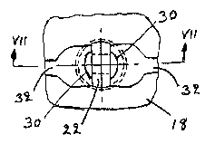
45. With regard to each hole as shown by Figure 18, the
10 pin 46 extends diametrically across the hole and each of
the conductor lines 50 electrically contacts two axially
extending edges of a respective terminal provided by a
conductor 44 lying within the hole. In fact, corners at
the edges of the conductors 44 may cut into the conductor
15 lines 50 during assembly so as to provide a gas-tight
effective connection. Subsequently, gaps defined between
the conductors 44 and the conductor lines 50 are filled
with solder 70 so as to secure the pin 46 in position and `-
also to provide an effective and permanent electrical con-
20 nection between each conductor line 50 and its conductor
terminal 44 within the hole. Each conductor line 50 is
thus electrically connected with an individual circuit line
42 on each side of the board. The soldering operation may
be performed by known soldering techniques, e.g. by the use
25 of vapor phase soldering techniques to~ether with a solder
doughnut disposed upon an upper end oE the pin and which is
caused to flo~ along the gaps upon melting of the solder.
It has been found that with the use of solder, wi~h each
electrical conductor 44 connected securely to its conductor
30 line 50, no electrical connection is formed by the solder
around the body 48 between one conductor line 50 and the
other.
With the pin 46 described above, the dimension
along the major axis across the section 52 may be suitable
35 for insertion into a 0.040 inch diameter hole and is com- ;
parable to dimensions of conventional all metallic circuit
board pins. While the dimensions are comparable, the pin
46 does provide two completely electrically isolated con-
~. ~ : . ... ..
. : :- -
.. ..
;? ,~
ductor lines 50. The plastics materlal of the body pro-
vides the required strength for the body for handling and
pin insertion purposes while the conductor lines 50 need
only have sufficient cross-sectional area for their
5 electrical requirements. The thickness of each of the
conductor lines 50 may only be in the region of 0.005
inches. Thus there is a small cross-sectional area of
conductor line 50 on each side of the body 48 and, as a
result, a minimized resistance to the passage of electrical
lO signals along the conductor lines.
With the two conductors 44 provided at each hole
in the board for connection to an individual pin 46 or
alternatively for use as through-hole conductors, an ex-
tremely dense circuitry arrangement may be provided with
15 the electrical conductors at each hole being disposed ex-
tremely closely together and with each hole diameter being
sufficiently small to accommodate one of the pins 46. For
a required circuitr~ arrangement, the size of the printed
circuit board is accordingly minimized.
When the conductors 44 are to be used as through-
hole conductors, masking plugs ma~ be caused to remain in
each of the holes. However, these plugs need to be of
different design from the plugs 22 in that they must be
contained wholly within each of the holes 14 so as not to
25 extend outwardly beyond the conducti~le material on each
side of ~he board.
In a modi~ication o~ the pins 46, the body 48 may
be formed of other dielectric material such as fiber~lass
or a ceramic.
In a modification of the first embodiment as
shown in Figures l9 and 20, a printed circuit board 72 is
provided with two electrical conductors 44 within each of
its holes 40 as described in the first embodiment.
However, the board 72 is provided with two individual
35 circuit lines 74 extending to each of the holes 14 in the
board. Each of the circuit lines 74 i~ electrically con-
nected, one to each of the electrical conductors 44. In
this modification, the electrical conductors 44 serve the
.~
~ , : .
14
sole function of providing terminals Eor pins similar to
the pins 46 described in the first embodiment and therefore
outside circuit line connections upon the board and to the
conductors 44 are not required. In this case the silk
5 screen masking arrangement on each surface of the board has
resulted in removal of sufficient copper material to result .
in two terminal pads 76 (Figure 20) each forming an ex- :
tension of its associated terminal 44. As shown by Figure
19, each of the terminal pads 76 is composed of the layers
10 12, 16 and 32 of copper material together with the tin/lead
layer 34, each layer being provided in the manner described
in the first embodiment.
In a second embodiment as shown by Figures 21, 22
and 23, printed circuit board 78 (Figures 23) is formed
15 from a substrate 80 (Figure 21) having upon each side sur-
face a preformed layer (not shown) of copper as described ~
in the first embodiment. After a layer of copper is laid ~.
over all surfaces by an electroless process and provides an
extra thickness layer 82 of 0.0001 to 0.0002 inches which
20 extends around the inside surface of the hole in a similarmanner to the layer 14 in the first er~odiment, then dia--
metrically opposed circumferentially e~tending regions 8~ :
o~ the layer 82 are removed as shown by Figure 21. Regions
84 may extend also into the material of the substrate
25 itself, but preferably should not do so, because of de-
lamination problems which may result in the fiberglass of
the substrate. However, to distinguish in the drawings,
the process of this embodiment from the first embodiment,
the regions 84 are, indeed, shown as extending into the
30 substrate althou~h in practice this is not advisable. The
material at the regions 84 may be removed by milling, rout-
ing, broaching or laser cutting techniques. The removed
regions 84 are of such a size as to comfortably accept a
section 52 of a pin 46 when the pin is pressed into the
35 hole as shown in Figure 24. The copper on the two surfaces
of the board is then covered in regions where copper con-
ductors are not required in the finished board by a silk
screen layer 86 as shown in Figure 21 so that copper
~ ' ~
: . ~
- . ~
remains exposed upon each surface in regions 88 where cir-
cuit lines are to be provided to each of the holes 81.
Subsequently, as shown in Figure 22, a further conductive
layer 90 is applied by electroplating upon the regions 88
5 and a layer 92 of copper is also applied by electroplating
upon the electroless layer 82. A section through the board
with the respective layers then resembles that of Figure 7
in the first embodiment with the masking plug in Figure 7
omitted. A final deposition is then made with an etch
10 masking material, i.e. tin/lead, to provide an overlying
layer 94 (Figure 23) upon the layer 90 and a layer 96 of
tin/lead is formed upon the layers 92 within the hole. A
section through the board 80 at this stage then resembles
Figure 9 in the first embodiment with the masking plug 22
15 removed. The silk screen layer 86 is then removed from -
each side of the board and the copper material underlying
the silk screen is thPn removed by conventional etching
techniques. This results in circuit lines on the board
surfaces underlying and including the layers 94, and
20 arcuate electrical conductors 97 within each hole extending
circumferentially around the hole and spaced apart from
each other. Each of the conductors 97 is formed from the
preformed copper layer and the electroless layer together
with the layers 92 and 96 in the manner described above.
With each conductor 97 acting as a terminal with-
in its respective hole (Figure 24), a pin 46 is inserted
into each hole and extends diametrically across it and into
the two removed regions 84 with each conductor line 50
electrically abutting edges of a respective conductor 97.
30 In Figure 24 each conductor terminal 97 is sectioned as a
single layer for clarity~ Subsequently gaps formed between
the conductor terminals 97 and the conductor lines 50 are
filled with solder 98 so as to secure each pin in position
and also to provide an effective electrical contact between
35 each conductor line 50 and its respective conductor ter-
minal 97. The soldering operation may be performed by
known soldering techniques as explained in the first em-
bodiment.
.: ,
: :
" ~
16
In further embodiments now to be described, while
more than two electrical conductors are described within
each hole of a printed circuit board, the size of each hole
and its respective circuit board pin for use with the hole,
5 may, because of manufacturiny restrictions need to be
larger than those described in the first and second embodi-
ments.
In Figure 25, there is shown a plan view of a
printed circuit board 100 having four individual circuit
10 lines 102 on each side (one side only being shown) of the
board. Each circuit is integral with an electrical con-
ductor 104 which extends along each hole on the sur~ace
thereof. Each electrical conductor extends
circumferentially of the hole as shown in Figure 25 and is
15 electrically isolated by being circumferentially spaced
from adjacent electrical conductors.
While the steps in the manufacture of the board
100 may be similar to those described in the first embodi-
ment by using masking plugs to mask parts of each hole upon
20 which electrical conductors are not required, clearly the
plugs 106 themselves, as shown by Figure 26, are of differ-
ent shape from the plugs 22 described in the first embodi-
ment. As shown by Figure 26, each plug is substantially
cruciform in cross-section with arms 108 providing the
25 maskad regions of the hole surface and upon which copper
material should not be deposited. Figure 26 does not show
the detail of the layers of each of tha conductors 104 as
is shown in previous embodiments, but it should be under-
stood that each conductor 104 is composed of an underlying
30 copper layer which has been electrolessly deposited, an
overlayer of electroplated copper material. This is the
composition of each conductor 10~ in the stage at Figure 26
with the mask in position. Subsequently, a tin/lead layer
would also be applied to cover the electroplated layer
35 prior to removal of the plugs 106 and masking material
present upon the two sides of the board. Etching would
then follow to remove the unwanted copper material within
the holes and upon surfaces of the board substrate.
. .
- ~ . . :
, . . .
.
. . .
17
A printed circuit board pin 110 for use with the
printed circuit board lOn of the third embodiment is of
definite length as shown by Figure 27 and comprises a di-
electric body 112 which carries four relatively electrical-
5 ly isolated con~uctor lines 114 extending along the length ,
of the body. These are clearly shown in Figures 27 and 28.
The body is molded from a urethane material or from any
other suitable dielectric material, and has tapered ends
116. The conductor lines 114 are of substantially
10 rectangular shape as shown in Figure 2~ and are laterallyspaced-apart around the substantially circular periphery of
the body and lie in recesses 118 of the body so as to pro-
trude slightly from the surface of the body.
The conductor lines 114 may be formed by a plat-
15 ing process, the stages of which are shown in Figures 29and 30. After the body 112 has been preformed by molding
techniques, which also provide the longitudinally extending
recesses 118, the peripheral surface of the body is masked
by the use of a suitable masking material 120 between the
20 recesses 118. This is shown in Figure 29. After masking,
the conductor lines 114 (Figure 30) are built-up within tha
recesses 118 by conventional plating techniques from copper
and to the required depth. After removal of the masking
material the cross-sectional shape of the pin is as shown
25 in Figure 28.
Each of the pins 110 is inserted into its in-
dividual hole 106 in tha printed circuit board. When
inserted into position, the conductor lines 114 engage the
conductor terminals 104, one to each conductor as shown by
30 Figure 31. The conductor lines 114 may be soldered to
their respective terminal conductors 104 by the use of a ~'
doughnut of solder, as in the first embodiment together
with vapor phase soldering techniques. Alternatively, the
plastic of the body 112 of each pin may have a certain
35 compressive resiliency to allow for an interference com-
pliant fit within its hole with each conductor line 114 in
gas-tight engagement with its respective terminal conductor
104.
::
-, ~
;
,; . " ' ~ ' ~' . ,
18
In a fourth embodiment as shown in Figure 33, a
printed circuit board 122 comprises a plurality of pin
receiving holes 124. Each pin receiving hole 124 has a
main hole portion 126 of large diameter to accept a pin and
5 a plurality, namely four, secondary hole portions 128 of
substantially smaller diameter which are interconnected
radially with the main hole portion 126 alon~ the length of
the hole. Each secondary hole portion 128 has upon its
surface a conductor terminal 130. As may be seen from
10 Figure 33, each conductor terminal 130 has ends at posi-
tions of intersection of the secondary hole portion with
the main hole portion, the ends exposed at the circum-
ference of the main hole portion.
Each hola 124 is formed initially by providing
15 four secondary holes 132 as a group 134 with the holes
spaced apart at the corners of an imaginary square around
the a~is of the hole 124 to be provided. Continuous co~-
posite conductive layers 136 composed of a first layer of
electrolessly deposited copper and then a second copper
20 layer by electroplating are then formed so as to completely
cover the surfaces of the holes 132. An overlying tin/lead
la~er is also provided to protect the underlying layers
during etching when certain conducti~e material on the
outer surfaces of the board is removed (as described in
25 other embodiments) to provide indiviclual circuit lines to
each conductor 136. This is the situation shown by Figure
32. Subsequently, the main part 126 of the hole 124 is
formed, the periphery of the main part 126 interesting the
peripheries of the holes 132 so as to cause interconnection
30 between the main and secondary hole portions as described
above. During formation of the main hole part 126, a
circumferentially extending section of each of the con-
ductors 136 is removed to produce the conductor terminals
130 with terminal ends exposed at the circumference of the
35 major hole portion 126 as has already been described.
Figure 34 illustrates a circuit board pin 138 for
insertion into each of the holas 124~ ~s is shown by
Figure 34, the circuit board pin 138 is of square or
.
19 ~ .
rectangular section and has longituclinally flat sides 1~0.
Junction regions between the sides 140 are recessed to
accommodate conductor lines 142 which extend longitudinally
of the pin. These conductor lines are substantially L-
5 shaped with two legs of each line lying in a recess of theplane of the adjacent side 140. The lines 142 are con-
veniently formed by plating techniques similar to that
described with reference to Figures 28 to 30.
As may be seen from Figure 35, a circuit board
10 pin 138 is inserted into each of the holes 124. When each
pin has been forced into position, each conductive line 142
is in gas seal-tight engagement with the two axially ex-
tending ends of corresponding conductor terminals 130 which
are exposed at the circumference of the main portion 126 of
15 the hole. Gaps between surfaces of the conductor lines 142
and the conductor terminals 130 are then filled with solder
144 by conventional soldering operations. The solder pro-
vides acceptable electrical continuity between the con-
ductor lines 142 and the conductor terminals 130. As dis-
20 cussed above in previous embodiments, with the solderingoperation, the solder is not caused to flow around the pin
so that there is no electrical bridging between one con-
ductor terminal 130 and the next~
As may be seen from the above embodiments, the
25 invention is concerned with a printed circuit board having
two or more electrical conductors associated with each hole
and which serve individual circuit lines extending towards
the hole. While the embodiments described illustrate the
use of two or four such electrical conductors, in other
30 embodiments there may be different numbers of conductors
provided at each hole, for instance three or five con-
ductors or more. The number of conductors which may be
provided for each hole is subject to the practicalities of
commercial manufacture involved in the provision of the
35 numbers of conductors for each hole, the numbers of circuit
lines which it is practically possible to extend to each
hole, and the resultant minimum size of each hole capable
of being provided with the required number of conductors.
. .
' ;`' , :~
,
;
, .
: ' ~ . ` ,; ' 1 ~ . ~ ' ,