Note: Descriptions are shown in the official language in which they were submitted.
202~676
This invention relates to a television system con-
verter which converts a hlgh-deflnition televislon slg-
nal into an NTSC signal of the present television
system.
A hlgh-definltlon televislon system, which is dif-
ferent from the present televlslon system ln an aspect
ratio, a number of scanning llnes, and a frame fre-
quency, has been developed. As one of example, there is
a MUSE (Multiple Sub-Nyquist Sampllng-Encodlng) system.
The MUSE system ls dlsclosed ln INTERNATIONAL
BROADCASTING SYMPOSIUM ON RADIO AND TELEVISION
ENGINEERING 1985 SESSION 2-~7) "Transmlssion of HDTV by
MUSE system" by Yulchl Nlnomlya et al.
The transmlsslon of MUSE slgnals ln thls system by
a broadcastlng satelllte was planned, and ls now in the
stage where such the transmlsslon ls put to practlcal
use. To recelve MUSE slgnals and see them as an lmage,
a MUSE decoder and a MUSE dlsplay are requlred. How~
ever, lt wlll take tlme to spread the MUSE decoder and
MUSE display wldely among common vlewers. Therefore,
there can be consldered a devlce whlch can receive MUSE
slgnals and convert the slgnal of the system lnto an
NTSC system, and see an lmage on a dlsplay of NTSC
system.
In case of convertlng the MUSE slgnal lnto the NTSC
slgnal, a point to notlce ls that the field frequency
of the MUSE signal ls 60 Hz and that of the NTSC signal
36 76
-- 2
ls 59.94 Hz.
Another polnt to notlce ls that a frequency of
the horlzontal scannlng llne of the MUSE slgnal is
30 x 525 = 15.75 KHz and that of the NTSC slgnal ls
sg.94 ~ 2 x 525 = 15.734 KHz. Also, a frequency of
color sub-carrler fsc ls deflned to a 1~2 multlple of
the integral of one period of the horizontal scanning
line, that is, 455/2.
If the televlslon slgnal havlng fleld frequency of
60.00 Hz ls used slmllar to NTSC system, color sub-
carrler fsc~ ls 60.00/59.94 x fsc. The color sub-
carrler fsc' has dlfferences of about 1000 ppm as
compared wlth the sub-carrier fsc of the NTSC slgnal.
In general, the frequency draw-ln range of the
color sub-carrler ln a televlslon recelver ls about
fsc ~ 400 Hz (= 100 mmp). If there are about lOOOppm
dlfferences, such a frequency cannot draw ln the color
sub-carrler. Therefore, lf the color sub-carrler havlng
such a dlfference ls input lnto a color signal proces-
sor, a color klller clrcult ls operated, so that an
lmage becomes monochrome.
To overcome thls problem, lf a normal color
sub-carrler fsc ls forced to use, the relatlonshlp
of an lnterleave between a lumlnance slgnal such as
a reference NTSC slgnal and the color sub-carrler
cannot be completely malntalned. As a result, lnterrup-
tlons such as a cross color and a cross lumlnance are
:
;
:
.
202367~
frequently generated in a recelver.
An ob~ect of the present inventlon is to provide a
television system converter which can prevent an image
from becoming monochrome in a receiver, and which can
reduce interruptions such as a cross color and a cross
luminance.
To attain the above ob~ect, the present invention
comprises:
scanning line processing means, to which a first
television signal whose frame frequency is different
from a television signal of the standard system is
supplied, for converting the first television signal
into an interlaced scanning luminance signal and two
interlaced scanning color-difference signals with a num-
lS ber of scanning lines which are smaller than the televi-
sion slgnal of the present standard system;
digital/analog converting means for converting the
interlaced scanning signals output from the scanning
llne processing means into analog signals, respectlvely
flrst synch regenerating means, to which the flrst
televlsion signal ls supplled from an input terminal,
for generating a sampling clock of the flrst television
signal;
phase-locked loop means for generating a color sub-
carrler and phase-synchronlzlng the color sub-carrler
wlth the clock lnput from the flrst synch regenerating
means; and
~236~6
quadrature modulating means, to which the two
color-different analog signals obtained from digital/
analog converting means are lnput, for modulatlng the
two color-dlfferent analog slgnals by the color sub-
carrier from the phase-locked means.
The color sub-carrier ls converted into the fre-
quency draw-ln range of a next stage television system
ln connection with the phase-locked means, the first
synch regenerating means, and the quadrature modulating
means.
Thls lnventlon can be more fully understood from
the followlng detalled descrlptlon when taken ln con-
~unction with the accompanying drawings, in which:
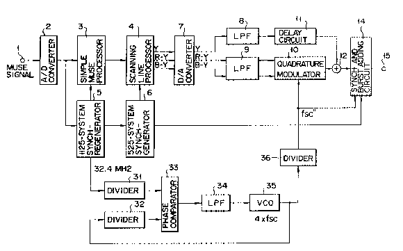
Fig. l is a block diagram showlng one embodiment
of the present lnvention;
Flg. 2 ls an explanatory drawlng showlng an example
of the dlsplay of the system-converted MUSE slgnal; and
Flg. 3 ls a dlagram speclflcally showlng a slmple
MUSE processor of Flg. l and a scannlng llne processor.
An embodlment of the present lnventlon will be
explalned wlth reference the drawlngs.
Flg. 1 shows one embodlment of the present
lnventlon. A MUSE slgnal, which ls recelved by a
tuner, ls lnput to an lnput termlnal 1 and supplled to
an analog to dlgltal ~herelnafter called A/D) converter
; 2. A dlgltal MUSE slgnal, whlch ls converted by an A/Dconverter 2, ls supplled to the simple MUSE processor 3
'' . ' ~ ':
. . . ., . , :
202367~
and 1125 system synch regenerator 5.
In the simple MUSE processor 3, a false orlglnal
high-difinltion signal is decoded. A clock, a tlmlng
slgnal, and a control slgnal, which are necessary to
perform the MUSE processing, are generated by 1125 sys-
tem synch regenerator 5. The clock, the tlming signal,
and the control signal are supplled to the simple MUSE
processor 3, a 525 system synch generator 6, and a fre-
quency divider 31.
The hlgh-definltion television signal, which is
decoded by the simple MUSE processor 3, is input to a
scanning line processor 4, and the number of scanning
lines is changed from 1125 to 400. The reason why the
number of scanning lines is not changed from 1125 to 525
ls that the aspect ratio of the high-definition televi-
sion signal is 16:9, so that a state of display as shown
ln Flg. 2 ls requlred ln order to pro~ect the lmage ln
the present televlslon recelver. However, slnce the
synch system of the output slgnal of the scannlng llne
processor must be 525/frame, the scannlng llnes of about
125 ln the upper and lower portlons of the dlsplay are
dlsplayed as black or gray as shown ln Flg. 2. In
other words, lf the aspect ratlo of the MUSE slgnal ls
malntalned, space reglons are generated ln the upper and
lower portlons of the dlsplay.
The 525 system synch generator 6 generates the
clock, the tlmlng slgnal, and the llke, whlch are
2~2~676
-- 6 --
necessary ln the scanning line processor 4, by use of
the timlng slgnal supplled from the 1125 synch regenera-
tor 5. However, since the converslon of the frame fre-
quency is not considered ln a MUSE-NTSC converter, the
frame frequency is 60.00 Hz and the frequency of the
horizontal scanning line ls 30 x 525 = 15.75 KHz.
The lumlnance signal Y, whlch is output from the
scanning line processor 4, and the color-dlfference sig-
nals (R - Y slgnal and B - Y slgnal) are lnput lnto a
dlgltal-to-analog (herelnafter called D/A) converter 7
and converted lnto analog slgnals. The analog lumlnance
slgnal Y ls supplied to a low pass fllter (LPF) 8 and (R
- Y) slgnal and (B - Y) signals are supplled to a low
pass fllter 9.
Two color-dlfference analog slgnals, whlch are out-
put from the LPF 9, are input into a quadrature modula-
tor 10 and modulated by a color sub-carrier fsc'', whlch
is supplied from a divider 36. on the other hand, the
analog luminance signal Y, whlch is output from the LPF
8, ls time-ad~usted by a delay circult 11 and lnput into
an adder 12. In the adder 12, the tlme-ad~usted luml-
nance slgnal and a carrler-color-dlfference slgnal
(chromlnance slgnal)~ whlch ls supplled from the quadra-
ture modulator 10, are synthesized.
In the ~uadrature modulator 10, two sub-carrlers,
whose phase are different from each other, are generated
by use of the color sub-carrler fsc''. The two
.
~23676
sub-carriers are modulated by the correspondlng color-
difference analog slgnals, respectively. The modulated
two signals are synthesized, output as the above-
mentloned carrler-color-difference signals, and input
into the adder 12.
The output signals of the adder 12 are supplied to
a synch and burst adding circuit 14. The synch and
burst adding clrcuit 14 adds various control slgnals
such as a synch signal, and a burst signal into the
signals, which are supplied from the adder 12 and gener-
ates a decode video signal, and supplies the signals to
an output terminal 15.
The above-mentioned sub-carrier fsc~' is generated
by a phase-locked loop circuit, which comprises dividers
31, 32, a phase comparator 33, a low pass filter 34, a
voltage controlllng osclllator (VCO) 35 uslng crystal,
and a dlvlder 36 ln the followlng manner.
The slgnal, whlch ls output from the 1125 system
synch-regenerator 5, ls a clock of 32.4 MHz (~ 960 S/H x
1125 x 30 Hz), which is necessary for performing the
slmple M~SE processing. The slgnal ls also supplled
to the dlvlder 31 and dlvlded (1/12000). On the other
hand, the output of the VOC 35, whlch osclllates quadru-
ple color-sub carrler frequencles, is dlvlded (1/5303).
The outputs of the dividers 31 and 32 are phase-compared
with each other by the phase comparator 33 and the high
frequency component is removed from the phase different
. ~ .
'' . ' ,, ' :, . .
. -
202367~
outputs through the LPF 34, and the outputs are supplied
to the control terminal of the VC0 35.
Thereby, the oscillation frequency of the VC0 35 is
phase-synchronized wlth the clock of the high-deflnltion
signal system.
As a result, the oscillatlon frequency 4fsc' of the
VCo 35 is as follows:
4fsc' z (32.4 MHz/12000) x 5303 = 14.318 MHz.
Therefore, the frequency fsc'' of the color sub-
carrler, whlch ls output from the dlvlder 36 for 1/4
dlvldlng ls as fullows:
fsc~ , 3.579525 MHz (false color sub-carrler).
Then, fsc " /30.00 = 119317.5.
Looklng fsc'' carefully, thls frequency value ls
a 1/2 multlple of the lntegral of the frame frequency of
30.00.
; Therefore, it turns out that the color sub-carrlerfsc" ls a signal whlch ls lnverted every frame of the
NTSC slgnal.
A normal sub-carrier fsc is as follows:
fsc . 525 x 59.94/2 x 455/2 - 3.579542 MHz.
Therefore, the dlfference between the above-
mentloned fsc" and fsc ls as follows:
(fsc - fsc" ) / fsc x 1000000 = 4.7 ppm.
Thls value fully satlsfies the draw-in frequency
range, fsc + 400 Hz (+ 100 ppm), of the color sub-
carrler of the televislon receiver of the NTSC eystem
~2~676
connected to the MUSE-NTSC converter.
In the above embodiment, the divldlng ratlos of two
dividers 31 and 32 have been set as follows:
1/12000, 1~5303, fsc~ = 3.579s2s MHz.
However, Table 1 shows the combinatlons showing the
case whlch satlsfies the followlng three conditions:
The color sub-carrier fsc~ satisfies the draw-in
frequency range, fsc + 400 Hz, of the color sub-carrier
of the television receiver of the NTSC system;
The color sub-carrier fsc " ls a 1/2 multlple of
lntegral of the frame frequency (30.00 Hz); and
The divldlng ratlos of the dlvlder 31 of 32.4 MHz
and the dlvlder 32 of 4fsc" are respectlvely small.
Table 1
Dividing Dlvlng Dlfference
fsc" Ratlo Ratlo ppm between
_ of 32.4 MHz of 4fsc'l fsc and fsc "
3.579255 1/60000 1/26513 -80.2
3.579375 1/4320 1/1909 -46.7_
3.579795 1/20000 1/8839 70.7
Accordlng to the above embodlment, the conversion
of the frame frequency of the flrst televlslon slgnal
~for example, MUSE slgnal) ls not performed. In other
words, the fleld frequency of 60.00 Hz ls malntalned and
the color sub-carrler ls locked to the phase reverslng
agalnst the frame frequency. Thereby, lnterference of
the color frequency band such as a cross color ln the
'
: '
6 7 6
-- 10 --
display receiver and a cross luminance can be prevented.
According to the present inventlon, the frequency
of the color sub-carrier can be set to the frequency
reversing every frame as the field frequency of the
input television signal is maintained. Also, the fre-
quency of the color sub-carrier can be set to the fre-
quency draw-in range in the color signal processor of
NTSC system. Moreover, in the present apparatus, a mem-
ory having a large capaclty ls not requlred and an image
can be prevented from becoming monochrome, and interfer-
ence such as a color cross and a cross luminance can be
reduced.
As a method for reducing interference such as the
cross color and the cross lumlnance, lt can be consid-
ered that the field frequency of the output signal of
the scannlng line processor 4 is co~verted from 60.00 Hz
to 59.95 Hz and is corrected to a reference NTSC signal.
To accomplish thls method, a memory having a large
capaclty for convertlng the frame frequency ls provided
between the scannlng llne processor 4 and the D/A
converter 7. Then, the output slgnal of the scannlng
llne processor 4 18 wrltten ln the frame memory wlth
the clock of 60.00 HZ x n and readout wlth the clock of
59.94 Hz x n. n (number of samples durlng lH) ls
approxlmately 1000 x 525.
However, accordlng to thls method, a memory of one
frame ~about lO00 samples /H) x 525 x 8 blts x 2 (for
.' ' ' ~ '~:,; ' ' "'
.
'' ~ , '.
, ~ . . . ..
~36 ~6
a lumlnance slgnal and a color signal) ls required only
for the conversion.
It can be said the above converter ls not a simple
MUSE-NTSC converter, which simply converts an MUSE sig-
nal into an NTSC signal.
In contrast, according to the embodiment shown inFig. 1, a memory having a large capacity is not
required, and interference such as a cross color and a
cross luminance can be reduced.
The reason why the word "simply~ is used is as
follows:
In the MUSE system, an image signal of one frame ls
divided into four fields, and transmitted as an MUSE
signal. Therefore, it is necessary to superimpose data
of four flelds. However, to superimpose data of four
fields, a large number of memories are required, and the
cost of the apparatus ls increased.
For thlæ reason, ln the slmple MUSE processor 3,
the calculatlon of the data of the surrounding plcture
elements ln the same filed can be performed.
Flg. 3 shows the lnner parts of the simple MUSE
processor 3 and the scannlng llne processor 4.
An MUSE slgnal, whlch ls dlgltlzed by clock rate
of 16.2 MHz, ls supplled to an lnput termlnal 201.
The MUSE slgnal ls lnput to an lnterafleld interpola-
tion circult 202 and 1125 system synch generator 5.
The intrafleld lnterpolatlon clrcult 202 performs
~ ' :
.- : ~ - .
: ' ' .
2~23676
- 12 -
an interpolation processing by use of the surrounding
pixels in the same fields. The lnterpolated slgnal ls
lnput to a TCI (time compressed integratlon) decoder
203. The TCI decoder 203 outputs two color dlfference
5 slgnals, which are multlplled durlng the horlzontal
blanklng perlod of the lumlnance slgnals, to be extended
to the tlme axls. The lumlnance signals Y, (R - Y),
(B - Y) are lnput to the followlng scanning llne proces-
sor 4.
A tlmlng slgnal ls supplled to the scannlng line
processor 4 from 1125 system synch generator 5 and 525
system synch generator 6. The scannlng llne processor
4 comprlses a scanning llne converter 204 and an lnter-
lace converter 205. The scannlng llne converter 204
converts 1125 sequentlal scannlng llne slgnals lnto 525
sequentlal scannlng llne slgnals. The converted luml-
nance slgnals Y, (R - Y), (B - Y) are supplled to the
lnterlace converter 205. The lnterlace converter 205
converts 525 sequential scanning llne signals into 525
lnterlaced scannlng signals. The lnterlaced scanning
signals, luminance signals Y, ~R - Y), ~B - Y) are lnput
to low pass filters 8 and 9 shown ln Flg. 1.
The above embodlment explalned that the slgnals to
be lnput to the scannlng llne processor 4 were MUSE slg-
25 nals whlch was slmply generated. However, the presentlnventlon ls not llmlted to these slgnals. If the slg-
nals are televlslon slgnals whlch are different from
. - -
.
.
~3676
the television signal of standard system ln the frame
frequency, the apparatus of the present invention can be
used.
., . . - .
: ., ~ .. ..
, . . .