Note: Descriptions are shown in the official language in which they were submitted.
~3678
1 Title o~ the Invention
SEMICONDUCTOR DEVICE
Back~round of the Invention
(Field of the Invention)
The present invention relates to a semiconductor
device used in a light reception circuit section or the
like in an optical data link or an optical CATV system.
(Description of the Related Background)
A conventional light reception circuit of this type is
shown in Fig. 1, for example. A light signal is received
by a light-receiving element 1 and converted into a
voltage signal by a resistor RL. A direct-current
component is removed by a capacitor Cc from the reception
signal which is converted into the voltage signal, and the
reception signal is amplified and demodulated by an
amplifier 2. The resistor RL, the capacitor Cc, and the
amplifier 2 are formed on the same integrated circuit (IC)
chip 3. Generally, the resistor RL has a resistance of
several hundreds ohms to 10 kQ , and the direct-current
component cutoff capacitor Cc has a capacitance of several
pico-farad to several hundreds pico-farad. A junction
capacitance CPD of about 0.5 pF is present in a p-n
junction of the light-receiving element 1, a floating
capacitance CCG (to ground) is present in the capacitor
Cc, and an input capacitance CI N is present in an input
section of the amplifier 2. When an input resistance of
2~3`6378
1 the amplifier 2 is given by RIN,
a high-pass cutoff frequency FH and a low-pass cutoff
frequency FL of the reception signal are expressed by the
following equations, respectively.
FH = 1/[2~ (RL//RIN)- (CPD + CIN + CCG)] . . . (1)
FL = 1/[2~ (RL//RIN)- Cc] ...(2)
Figs. 2(A) and 2(B) show the inside of a package when
the IC chip is packaged. Fig. 2(A) is a plan view of the
IC chip, and the Fig. 2(B) is a side view of the IC chip.
A common ground pattern 5 which is set at a common
reference voltage for the circuit is formed on a ceramic
substrate 4, and IC chip 3 is die-bonded on the ground
pattern 5 through a back metal formed on the back of the
IC chip 3. A reference potential of an inner circuit of
the IC chip 3 is set to be equal to a potential of the
ground pattern 5 by means of a boding wire. A signal
terminal pattern 6 electrically isolated from the common
ground pattern 5 is wire-bonded with external terminals of
the IC chip 3 and electrically connected to frame lead
pins.
In the above conventional device arrangement, when the
resistance of the resistor RL is increased to improve
receiving sensitivity of the circuit, an S/N ratio showing
a signal-to-noise ratio is increased, thereby improving
the receiving sensitivity. However, as understood from
equation (1), the high-pass cutoff frequency FH is
decreased. ~hen the resistance of the resistor RL is
'' ~ "
2~:3678
1 constant, the high-pass cutoff frequency FH is increased
proportional to a decrease in capacitance of (CPD + CI N +
CCG) .
In order to decrease the low-pass cutoff frequency FL,
as understood from equation (2), when the resistance of
the resistor RL is constant, the capacitance of the
direct-current component cutoff capacitor Cc must be
large. For this reason, a electrode pattern 7 for the
capacitor Cc occupies a large area in the IC chip 3 as
shown in Fig. 3. Therefore, the floating capacitance CCG
present between the electrode pattern 7 and the ground
pattern 5 is increased, thereby decreasing the high-pass
cutoff frequency FH. In addition, when the capacitance of
the capacitor Cc is decreased to decrease the floating
capacitance CCG, the low-pass cutoff frequency FL is
increased, thereby increasing jitter.
Summar~ of the Invention
It is an object of the present invention to provide a
semiconductor device having a high receiving sensitivity
and a wide receiving band. According to the present
invention, a r-eception circuit for removing a direct-
current component of a reception signal by a capacitor is
incorporated in a semiconductor chip, a metal film is
provided on a back of the semiconductor chip, a first
conductive pattern set at a common reference voltage for
the circuit is formed on an electrically insulating
678
1 substrate, a second conductive pattern is formed to be
electrically insulated from the first conductive pattern,
the metal film of the semiconductor chip is fixed to the
second conductive pattern, and the voltage of the second
conductive pattern is equal to the voltage of the
capacitor of the reception circuit.
Therefore, a variation in voltage of the capacitor
formed within the semiconductor chip is substantially
equal to a variation in voltage of the second conductive
pattern underlying the capacitor. As a result, there is
almost no floating capacitance in the capacitor for
removing a direct-current component of the reception
signal. For this reason, a semiconductor device having a
high receiving sensitivity and a wide receiving band can
be provided. The device according to the present
invention is effectively employed to a high-speed and
wide-band communication system.
The present invention will become more fully
understood from the detailed description given
hereinbelow and the accompanying drawings which are given
by way of illustration only, and thus are not to be
considered as limiting the present invention.
Further scope of applicability of the present
invention will become apparent from the detailed
description given hereinafter. However, it should be
understood that the detailed description and specific
examples, while indicating preferred embodiments of the
20~3678
1 invention, are given by way of illustration only, since
various changes and modifications within the spirit and
scope of the invention will become apparent to those
skilled in the art from this detailed description.
Brief Description of the Drawin~s
Fig. 1 is a circuit diagram showing a light reception
circuit on a conventional IC chip mounted on a
semiconductor device;
Fig. 2A is a plan view showing the inside of the
semiconductor device on which the conventional IC chip
shown in Fig. 1 is mounted;
Fig. 2B is a side view showing the inside of the
conventional semiconductor;
Fig. 3 is a view showing a electrode pattern of the
conventional IC chip shown in Fig. l;
Fig. 4A is a plan view showing the inside of a
semiconductor device according to the one embodiment of
the present invention;
Fig. 4B is a side view showing the inside of the
semiconductor device shown in Fig. 4A; and
Fig. 5 is a circuit diagram showing a light reception
circuit on an IC chip mounted on the semiconductor device
shown in Figs. 4A and 4B.
Detailed DescriPtion of the Preferred Embodiment
Figs. 4A and 4B show an embodiment of the present
~23678
1 invention, in which Fig. 4A is a plan view and Fig. 4B is
a side view.
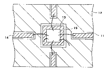
A ceramic substrate 11 is made of an electrically
insulating material such as alumina (Al203). The
substrate 11 is metallized by gold-palladium or silver-
palladium to form a ground pattern 12 in a wide area. The
ground pattern 12 is set at a common reference voltage of
each semiconductor circuit chip mounted on the substrate
11. The metal used in metallization is patterned by
etching techniques to form an island-like die area pattern
13 electrically isolated from the ground pattern 12. By
patterning, a signal terminal pattern 14 having an
elongated shape is formed to be electrically isolated ~rom
the ground pattern 12.
An IC chip 15 which incorporates a light reception
circuit is die-bonded on the die area pattern 13, and a
metal film formed on the back side surface of the IC chip
15 is electrically connected and fixed to the die area
pattern 13. The external terminals of the IC chip 15 are
wire-bonded on the signal terminal pattern 14, thereby
transferring a signal from the circuit to a frame lead pin
(not shown) connected to the signal terminal pattern 14.
one of the external terminals is wire-bonded on the die
area pattern 13.
Fig. 5 shows a circuit incorporated in the IC chip 15.
An external terminal 16 of the IC chip 15 is connected
to a light-receiving element 17 such as a photodiode
67~
1 outside the chip and connected to a resistor RL inside the
chip. That is, the light-receiving element 17 and the
resistor RL are connected in series with each other and
the resistor RL are electrically connected to the ground
pattern 12. The external terminal 16 is connected to one
terminal of a capacitor Cc inside the chip, and the other
terminal of the capacitor Cc is connected to the input
terminal of a buffer amplifier 18 which is a non-inverting
amplifier having a amplification factor of 1. The buffer
amplifier 18 is constituted by a source follower circuit
and the like, and an output from the amplifier 18 is sent
to an amplifier 19. The output terminal of the amplifier
19 is connected to an external terminal 20, and the
external terminal 20 is connected to a receiver (not
shown). The output terminal of the buffer amplifier 18 is
connected to an external terminal 21, and the external
terminal 21 is wire-bonded on the above die area pattern
13 to be electrically connected with the above die area
pattern.
In the above arrangement, when a light signal is
received by the light-receiving element 17, the light
signal is converted into an optical output current. The
optical output current is converted into a voltage signal
by the resistor RL, and then a direct-current component of
the voltage signal is removed by the capacitor Cc. The
reception signal from which the direct-current component
is removed is amplified and demodulated by the amplifier
~2~ 78
1 19 through the buffer amplifier 18. The demodulated
signal is sent to the receiver through the external
terminal 20. The reception signal output from the buffer
amplifier 18 is sent to the die area pattern 13 through
the external terminal 21. For this reason, the voltage of
the capacitor Cc is applied to the die area pattern 13.
Therefore, a variation in voltage of the capacitor Cc
is substantially equal to a variation in voltage of the
die area pattern 13 underlying the IC chip 15. That is,
the amplitudes of the voltages at the capacitor Cc and the
metal film formed on the back side of the IC chip 15 are
equal to each other, and the phases of their voltages are
equal to each other. In this case, a floating capacitance
CCG to ground (die area pattern 13) of the capacitor Cc is
parasitically formed between the electrode of the
capacitor Cc and the metal film (die area pattern 13).
That is, since the floating capacitance CCG defines a rate
of variation in charge accumulated between both the
electrodes to a variation in voltage applied between both
the electrodes, the floating capacitor CCG is not almost
present.
For this reason, the high-pass cutoff frequency FH of
the reception signal expressed in equation (1) can be
increased because the floating capacitance Cc G can be
neglected. The capacitance of the direct-current
component cutoff capacitor Cc can be increased regardless
of the floating capacitor CCG, and the low-pass cutoff
~3;6 78
l frequency FL expressed in equation (2) can be decreased.
Therefore, the width of a receiving band of the circuit is
increased. In addition, since the capacitance CCG is
decreased in equation (1) and the capacitance Cc is
increased in equation (2), the resistance of the resistor
RL can be increased, thereby improving the receiving
sensitivity of the circuit.
In the light reception circuit of this type, the low-
pass cutoff frequency FL is generally set to be less than
l/100 to 1/1,000 of the high pass cutoff frequency FN.
Therefore, in order to form a light reception circuit
having, e.g., a bandwidth of 500 MHz, the low-pass cutoff
frequency FL must be set to be less than 5 MHz. When a
minimum receiving sensitivity is set at -30 dBm, the
resistor RL connected to the light-receiving element 17 in
series must have a resistance of 1 kQ at least. In this
case, the capacitance of the direct-current component
cutoff capacitor Cc can be calculated by substituting each
constant in equation (2) expressing the low-pass cutoff
frequency FL as follows. In this case, since the
resistance of the resistor RL is sufficiently larger than
that of the input resistor RIN of the amplifier 19, the
resistance of the parallel combination resistor RL//RIN of
the resistor RL and the resistor RIN is substantially
equal to that of the resistor RL.
5 x 106 = 1/(2~ 1 x 10³- Cc)
.-. Cc = 31.8 pF
2~367~
1 A capacitance per unit area of a capacitor which can
be monolithically formed on the IC chip falls within the
range of about 0.05 to 0.1 fF/~ m2. In this case, even if
a capacitor having a capacitance per unit area of 0.1 fF/
~ m2 can be formed, the area of the capacitor Cc is
318,000 ~ m2.
In the conventional arrangement shown in Figs. 1 and
2, when the capacitor Cc having this area is formed, a
floating capacitance CCG (to ground) of the capacitor Cc
is as follows. In this case, assume that the IC is made
of gallium arsenide (GaAs), that the thickness o$ a GaAs
substrate is normally set to be 400 ~ m, and that its
specific dielectric constant ~ is set to be 13.
CCG = ~ (318,000 . 400) = 92 fF
The sum (CPD + CIN) of the junction capacitance CPD Of
the light-receiving element 1 and the input capacitance
CIN of the amplifier 2 falls within the range of 0.4 to
0.6 pF. For this reason, in a conventional device
arrangement, the ratio of the floating capacitance CCG to
the sum of the capac:itances is about 20%, and the floating
capacitance cannot be neglected. Therefore, the
denominator of equation (1) is increased, and the high-
pass cutoff frequency FH is decreased due to the influence
of the floating capacitance CCG. AS a result, the
bandwidth of the signal received by the circuit is
narrowed.
~owever, according to the present invention, the
~v36 78
1 variation in voltage of the capacitor Cc is substantially
equal to the variation in the die area pattern 13 as
described above. I'here~ore, even when the capacitor Cc
has the large area of 318,000 ~ m2, the floating
capacitance CCG is not almost present in the die area
pattern 13. For this reason, the bandwidth of the signal
received by the reception circuit is large, and the
receiving sensitivity of the circuit is improved.
From the invention thus described, it will be
obvious that the invention may be varied in many ways.
Such variations are not to be regarded as a departure from
the spirit and scope of the invention, and all such
modifications as would be obvious to one skilled in the
art are intended to be included within the scope o~ the
following claims.