Note: Descriptions are shown in the official language in which they were submitted.
' ) r~ r~ ~
BACKGROUND OF ~HE INVENTION
Field of the Invention
This invention relates generally to a magnetic head position
control system and, more particularly to a system in which the
magnetic head employed in recording a magneto-optical disk is
driven to maintain a constant distance between the recording
surface of the disk and the magnetic head.
Description of the Backqround
In a reeording apparatus for a magneto-optical disk in
general, an optical head and a magnetic head are disposed in a
eontaet-free fashion on opposing sides of the disk. The recording
apparatus operates in accordanee with a magnetic field modulation
system, whereby a magnetic field corresponding to the recording
signal is generated by the magnetic head and applied to the
magneto-optical disk, and the area of the disk that is subjected to
the magnetic field is heated by a laser beam from the optical head,
thereby effecting signal recording.
Because of the information density requirements and the
dimensions involved, the laser beam emitted from the optical head
must be properly focused onto the disk. The optical head generally
controls the focus by collecting focusing data produced by the
laser light irradiated onto and reflected from the recording area
of the disk, thereby producing a predetermined spot on the
~ ~ ~J ~d~
recording ~urface of the disk for recording. By this means, it is
possible for the above-described optical head to remain at a
constant distance from the magneto-optical disk even when the
relative position between the magneto-optical disk and the optical
head is changed due to fluctuations in the thicXness o~ the
magneto-optical disk, the rotating disX deviates from its in-plane
position, or the disk table adapted for rotating the disk is
tilted. In the absence of some means for detecting the relati~e
distance between the magnetic head and the magneto-optical disk,
the magnetic head must be mounted at a position sufficiently spaced
apart from the magneto-optical disk so that the magnetic head will
not contact the magneto-optical disk, even when the position of the
magneto-optical disk fluctuates in one or more of the above-
described fashions.
When the magnetic head is too far away from the magneto-
optical disk, the power consumption is disadvantageously increased
because the magnetic head must~generate a stronger magnetic field
for supplying the predetermined recording magnetic field to the
recording surface of the magneto-optical disk. In other words,
when the separation between the magnetic head and the magneto-
optical disk is excessive, an insufficient magnetic field will be
applied to the recording surface of the magneto-optical disk,
thereby increasing the error rate or lowering the S/N ratio. In
the worst of cases, recording may be unfeasible.
: For obviating the above inconvenience, an electrode may be
mounted on the ~agnetic head in opposition to the magneto-optical
,r ~.~ W P~ ~
disk for detecting changes in the relative distance between the
magnetic head and the disk based on changes in capacitance between
the disk and the electrode. The position of the magnetic h~ad may
be controlled by the detection output of the electrode for
maintaining a constant relative distance between the magnetic head
and the disk and to enable the magnetic head to be positioned in
the vicinity of the magneto-optical disk. Japanese Patent
Application Hei 1-214138 proposes a floating control of a
perpendicular magnetic recording system including a disX medium and
a stylus, which corresponds to a magnetic head.
However, when the changes in the relative distance between the
magnetic head and the disk are measured by the changes in
capacitance between the magneto~optical disk and the capacitance
detection electrode mounted on the magnetic head, the accuracy o~
the control of the magnetic head positi.on by the detection output
is affected by the linearity of temperature characteristics of the
control circuit, so that a predetermined relative distance between
the magnetic head and the disk cannot be maintained with accuracy.
OBJECTS AND SUMMARY OF THE INVENTION
Accordingly, it is an object of the present invention to
provide a magnetic head position control apparatus for use with a
magneto-optical disk that can eliminate the above-noted defects
inherent in previously proposed systems.
It is another object of the present invention to provide a
magnetic head position control apparatus in which changes in the
relative distance between the magnetic head and the magneto-optical
disk are detected from changes in capacitance between a capacitance
detection electrode mounted on the magnetic head and the magneto-
optical disk.
It is a further object of the present invention to provide a
position control system in which the magnetic head is accurately
maintained at a predetermined distance from the magneto-optical
disk, without being influenced by temperature characteristics or
nonlinearities of the control circuit.
According to an aspect of the present invention a magnetic
head position control apparatus includes a magnetic head in
opposition to the magneto-optical disk, an oscillator circuit
having an oscillation frequency that is variable as a function of
changes in capacitance between the capacitance detection electrode
and the magneto-optical disk, a phase locked loop type phase
detection circuit for detecting a phase difference between the
output of the oscillator c~r~uit and the output of a voltage
controlled oscillator having oscillation characteristics close to
those of the oscillator circuit, whereby the oscillation output of
the oscillator circuit performs feedback control of the phase of
the voltage controlled oscillator based on the output of the phase
detection circuit to form an ultimate detection output based
thereon, and a head driver, operating in response to the ultimate
detection output of the phase locked loop type phase detection
circuit to drive the magnetic head, as well as the capacitance
detection electrode, towards or away from the recording surface of
the magneto~optical disk.
In accordance with the ahove described magnetic head position
control apparatus, changes in the relative distance between the
magnetic head and the magneto-optical disk are detected in the form
of changes in capacitance between the capacitance detection
electrode attached to the magnetic head and the magneto-optical
disk. The oscillation frequency of the oscillator circuit changes
with changes in the capacitance. The phase locked loop type phase
detection circuit detects the phase difference between the
oscillation output of the voltage controlled oscillator forming a
portion of the phase locked loop type phase detection circuit and
the oscillation output of the oscillator circuit. It is by this
oscillation output that the oscillation output of the voltage
controlled oscillator is controlled in a feedback control fashion.
The voltage controlled oscillator has oscillation characteristics
similar to those of the oscillator circuit so that errors
ascribable to differences in temperature characteristics and
nonlinearities of the oscillator circuit and the voltage controlled
oscillator will not exist. The phase locked loop type phase
detection circuit produces a detection output corresponding to
changes in the relative distance between the magnetic head and the
magneto-optical disk, which is sent to the head driver as control
signals. The head driver, in turn, drives the magnetic head in
accordance with the control signals to malntain the relative
distance at a constant value.
,'' , f ~ .; . . ~ s
The manner in which the above and other objects, features, and
advantages are achieved by the present inveniion will become
apparent from the following description thereof, to be read in
conjunction with the accompanying drawings in which like reference
numerals represent the same or similar elements.
BRIEF DESCRIPTION OF THE DRAWINGS
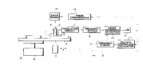
Fig. 1 is a block diagram showing the construction of a
~agnetic head position control apparatus according to an embodiment
of the present invention.
Fig. 2 is a perspective view of a capacitance cletection
electrode mounted on a magnetic head as employed in the magnetic
head position control apparatus of Fig. 1.
Fig. 3 is a cross~sectional view of the magnetic head shown in
Fig. 2.
Fig. 4 is a schematic diagram of an oscillator circuit
employed in the magnetic head position control apparatus of Fig. 1.
Fig. 5 is a schematic diagram of a voltage controlled
oscillator employed in the magnetic head control apparatus of Fig.
1. .
Fig. 6 a block diagram showing a magnetic head position
control apparatus according to another embodiment of the present
invention.
Fig. 7 is a illustrative diagram useful in explaining the
effects of stray capacitance on detecting the distance between the
magnetic head and the magneto-optical disk.
DETAILED DESCRIPTION OF PREFERRED EMBODIMENTS
Referring to Fig. 1, the recording apparatus for a
magneto-optical disk includes a magnetic head 2 and an optical head
3 arranged in a contact-free manner on opposing sides of a magneto-
optical disk 1 rotationally driven by a spindle motor ~. The
magnetic head 2 applies a recording magnetic field to a recording
surface 5 of the magneto-optical disk 1, which magnetic field
corresponds to a current that runs through a recording coil 4 from
a recording signal processing circuit (not shown). The optical
head 3 irradiates onto the recording surface 5 of the magneto-
optical disk 1 a laser beam that is generated from a laser diode
(not shown) enclosed in the optical head 3. The information to be
stored on the disk is recorded on the recording surface 5 by the
recording magnetic field and the laser beam. The magnetic he~d 2
and the optical head 3 are attached to a slider, not shown, so as
to be simultaneously driven radially across the disk 1 as indicated
by an arrow X. The magnetic heàd 2 and the optical head 3 may also
be moved in a direction towards or away from the recordiny surface
5 of the disk 1 as indicated by an arrow Y. The optical head 3 may
be controlled by a focusing servo in the direction shown by the
arrow Y.
The magnetic head position control apparatus of the present
invention regulates the position of the magnetic head 2 by moving
the magnetic head in a direction towards or away from the recording
surface 5 of the disk 1 as indicated by the arrow Y. This magnetic
head position control apparatus is hereinafter explained.
A capacitance detection electrode 6 is attached to the
magnetic head 2 facing the magneto-optical disk 1. This detection
electrode 6 is movable in the direction of the arrow Y along with
the magnetic head 2. A capacitance is generated between the
detection electrode 6 and the magneto-optical disk 1 as a function
of the relative distance between the electrode 6 and the disk 1.
Thus the changes in the relative distance between the disk 1 and
the head 2 may be detected ~y measuring the change in the
capacitance.
~ igs. 2 and 3 illustrate a concrete example of the
construction of the magnetic head 2 fitted with the capacitance
detection electrode 6. As shown therein, the magnetic head 2 is
formed by a core 20 having a U-shaped cross-section. A magnetic
yoke 21 in the form of a column is projected from the center of an
inner wall of' the web of the U-shaped core 20. A recording coil 4
is wound about the peripheral wall of the magnetic yoke 21. The
capacitance detection electrode 6 is formed of a s~uare-shaped
metallic plate having a central through-hole for receiving the
magnetic yoke 21. The capacitance detection electrode ~ is secured
to the ends of both arms of the U-shaped core 20 with the foremost
part of the magnetic yoke 21 passing through the through-hole.
When in use, the magnetic head 2 is mounted with the end of the
magnetic yoke 21 and the capacitance detection electrode 6 facing
the magneto-optical disk 1.
The ~apacitance detecti~n electrode 6 is connected to an
oscillator circuit 7 in the manner shown in ~ig. 1. The
' Ç~' tJ ~; "'' ~
oscillation frequency of the oscillato-r circuit 7 is variable as a
function of the capacitance changes detected by the capacitance
detection electrode 6 and is constructed as shown for example in
Fig. 4. Thus, the oscillator circuit 7 shown in Fig. 4 is an LC
oscillator circuit comprised of an amplifier 41, a coil 42
connected across the input and output terminals of the amplifier 41
and a pair of capacitors 43, 44 connected respectively between the
input and output terminals of the amplifier 41 and ground. The
capacitance of the capacitor 43 corresponds to the capacitance
between the electrode 6 and the disk 1. Thus, the oscillation
frequency of the circuit 7 changes as a function of the capacitance
change in the capacitor 43, that is, the capacitance change between
the electrode 6 and the disk 1. The oscillation output of the
oscillator circuit 7 is output from the amplifier 41 by means of a
buffer amplifier 45.
This oscillator circuit 7 is provided in proxi~ity to the
capacitance detection electrodè~6. By providing the circuit 7 in
proximity to the capacitance detection electrode 6, the effect of
any stray capacitance may be reduced. Also, by setting the Q of
the oscillator circuit 7 at a higher ~alue, the circuit 7 is less
susceptible to disturbances from the electro-magnetic field created
by the magnetic head 3 so that the circuit 7 may perform a more
stable control operation.
The oscillation output from the oscillator circuit 7 is
supplied to a phase locked loop (PLL) type phase detection circuit
3 which is comprised of a phase difference detection circuit 10, a
voltage controlled oscillator 11, and a low-pass filter LPF 13 or
the like. The oscillation output from the oscillator circuit 7 is
supplied to the phase difference detection circuit 10 by means of
a frequency divider 9, the oscillation output of the voltage
controlled oscillator 11 is supplied to the phase difference
detection circuit 10 by means of a frequency divider 12, and the
detection output of the phase difference detection circuit 10 is
fed back to the voltage controlled oscillator ll by means of the
LPF 13.
The voltage controlled oscillator 11 has oscillation
characteristics similar to those of the oscillator circuit 7, and
may be constructed, for example, as shown in Fig. 5. Thus, similar
to the oscillator circuit 7 shown in Fig. 4, the voltage controlled
oscillator 11 shown in Fig. 5 is comprised of an amplifier 51, a
coil 52 connected across the input and output terminals of the
amplifier 51, a capacitor 54 connected between the output terminal
of the amplifier 51 and ground, and a capacitor 53 connected
between the inp~t terminal of the amplifier 51 and a negative power
source -B by means of a variable capacitance diode 55. The
detection output of the phase difference detection circuit 10 is
supplied via LPF 13 to the ~unction between the capacitor 53 and
the variable capacitance diode 55, whereby the capacitance of the
diode 55 is variable as a function of the detection output. Thus,
the frequency of the oscillation output of the voltage controlled
oscillator 11, obtained at the output o~ the amplifier 51 by means
1 x ~ s~
of a bu~fer amplifier 56, changes as a function of the detection
output of the phase difference detection circuit 10.
This oscillation output from the voltage controlled oscillator
11 is transmitted via frequency divider 12 to the phase difference
detection circuit 10 for phase comparison with the oscillation
output that is supplied from the oscillator circuit 7. If any
phase difference is measured between these oscillation outputs, a
detection output corresponding to the phase difference is output
from the phase difference detection circuit 10 for feedback control
of the oseillation phase of the voltage controlled oscillator 11 to
decrease the phase difference. The detection output of the phase
differenee detection cireuit 10 of the PLL type phase detection
eircuit 8 finally is output as the detection output by means of LPF
13.
Thus an ultimate detection output is obtained from this ~LL
type phase deteetion circuit 8 as a function of changes in the
relative distanee d between the capacitance detection electrode 6
and the magneto-optical disk 1, that is, in the relative distanee
between the magnetic head 2 and the magneto-optical disk 1.
This detect.ion output is transmitted to a phase compensator 14
for phase compensation and thence to head drive means 15. The
drive means 15 operates, with the detection output as a control
signal, to drive the magnetic head 2, together with the capacitance
detection electrode 6, in a direction towards or away from the disk
1 as shown by the arrow Y by, for example electro-magnetic means,
11
' ?-~ ~ J j ~ ~
for maintaining a constant relative distance between the magnetic
head 2 and the magneto-optical disk 1.
In this manner, with the present magnetic head position
control apparatus, the control signal for the head drive means 15
is produced by the PLL type phase detection circuit 8, which
includes the voltage controlled oscillator 11 having oscillation
characteristics similar to those of the oscillation circuit 7.
Thus, any errors caused by different temperature characteristics of
the various circuit elements such as the coils 42, 52, or those
caused by nonlinear characteristics of the voltage controlled
oscillator 11 may be eliminated to realize a highly accurate
control operation. In addition, use of the PLL type phase
detection circuit 8 provides a high gain as compared with a control
circuit in which the oscillation output of the oscillator circuit
7 is directly converted into an electrical voltage for driving the
magnetic head 2 without the use of the PL~ type phase detection
circuit. Thus, the PLL type phase detection circuit provides a
highly accurate wide-range control operation.
In accordance with the above-described magnetic head position
control apparatus, a positioning servo operation is performed on
the magnetic head as a function of the capacitance formed between
the recording surface 5 (metal evaporated surface) of the magneto-
optical disk 1 and the capacitance detection electrode 6. However,
there is a risk that when the size of the disk 1 or the area of the
recording surface changes, the control operation may not result in
an optimum magnetic gap at all times.
12
Thus, the capacitance may be affected when the magneto-optical
dis~ 1 is loaded on the turntable, because stray capacitance Co may
form between the reflective surface, which may be aluminum foil,
formed by evaporation on the recording surface of the optical disk
and the turntable. Such stray capacitance Co would then cause the
oscillation frequency of the oscillation circuit 7 to change.
Since the stray capacitance Co changes marXedly with the outer
size of the magneto-optical disk loaded on the turntable and more
so with the area of the vaporized metal surface which forms the
recording surface of the magneto-optical disk, the rèlative
distance d from which the magnetic head is positioned from the disk
changes slightly with the size of the magneto-opt.ical disk, so that
the magnetic gap d cannot be initially set to an optimum value.
A magneto-optical head position control apparatus according to
the present invention, designed for obviating the above mentiolled
drawbacks, will be hereinafter explained.
Fig. 6 is a block diagram illustrating the above mentioned
magnetic head position control apparatus, wherein the same parts as
those of Fig. 1 are designated by the same reference numerals. ~or
example, numeral 1 denotes the magneto-optical disk, numeral 2
denotes the magnetic head mounted in opposition to the disk 1, and
numeral 3 denotes the optical head.
The output of the capacitance detection electrode 6 is
supplied to a C/V converter 21 for converting the capacitance
values into corresponding signal voltages. Although the C/V
converter 21 corresponds to the PLL type phase detection circuit 8,
as shown in Fiy. 1, it may also be constituted by other conversion
units.
Disk data detection unit 22 measures the detectlon data output
from the optical head 3~ The detection data output from the
optical head relates to the outer shape or the inside diameter of
the magneto-optical disk 1, that is, the area of the recording
surface on which a metal foil is deposited. This data is pre-
recorded on the lead-in area of the magneto-optical disk 1 in the
form of bit data.
A DtV converting unit 23 converts the detected data to a
voltage for selecting and outputting predetermined bias voltage
signals from the data of the disk data detection unit 22. The
output of this D/V converting unit 23 and the output of the C/V
converting unit 21 are su~med together at signal summiny point 24.
The summed data, which includes the predetermined bias signals from
the D/V converting unit 23, is transmitted to the servo circuit of
the magnetic head 2. '~
As the size ~ of the magneto-optical disk 1 increases as shown
in Fig. 7, the value of the stray capacitance Co between the disk
1 and the recording apparatus also increases as a general rule,
which results in the capacitance value detected at the magnetic
head 2 being increased. As a result, the servo circuit of the
magnetic head 2 will compensate for the increase in detected
capacitance by increasing the distance between the magnetic head 2
and the magneto-optical disk 1. In other words, the servo circuit
will increase the magnetic gap d. When the magnetic head 2 is
14
separated from the magneto-optical disk 1, the intensity of the
impressed magnetic field is lo~ered.
In such a case, the D/V converting unit supplies to the servo
circuit a bias signal, superimposed with the signal from the C/V
converting unit, which will reduce the strength of the control
signal to prevent the magnetic head 2 from being drawn too far away
from the magneto-optical disk 1.
When the magneto-optical disk 1 being employed is of a lesser
diameter, the stray capacitance Co becomes smaller so that by means
of the D/V converter 23 the magnetic head 2 is controlled to move
in the opposite direction to that described above, that is, the
servo circuit tends to narrow the magnetic gap d. It is not
desirable that the magnetic head 2 be closer to the magneto-optical
disk 1 than the predetermined distance d since the magnetic head 2
may contact the recording surface of the magneto-optical disk 1 on
application of a sudden impact on the magneto-optical recording
apparatus, resulting in in~ury to the head 2 or to the disk 1.
However, according to the present invention, when a small-
sized disk is loaded, the disk data detection unit 22 first reads
data from the disk indicating that the disk is of a smaller size,
and a bias signal suited to the disk size is supplied by the D/V
converter 23 to the servo circuit to control the position of the
magnetic head 2 to provide a magnetic gap d which will prevent the
above mentioned inconvenience from occurring.
In this manner, the servo circuit of the present invention for
controlling the magnetic head position is designed to compensate
for the effects of any stray capacitance Co generated by different
sized magneto-optical disks 1 that are loaded in the recording
apparatus. The servo circuit of the present invention will
automatically regulate the value of the bias signal output from the
D/V converter 23, so that the magnetic head may be controlled to
provide an optimum magnetic gap at all times.
The foregoing embodiment is useful when data relating to the
size or the inside diameter of the disk are previously input in the
lead-in area of the disk. Ho~-ever, the above-described embodiment
may be arranged similarly to the conventional multiple disk player,
50 that a disk size detection unit 25 for detecting the size of the
magneto-optical disk by a photosensor may be provided, and a bias
signal which will give the optimum magnetic gap for the particular
loaded disk is selected by the detection unit 25 and transmitted to
the signal summing point 24, as indicated by a broken line in Fi~.
6.
The bias signal supplied ~to the servo circuit may also be
input directly to the C/V converter 21, as shown by the dashed line
connection in Fig. 6.
According to the present invention as described above, various
predetermined bias signals which correspond to various sizes of
magneto-optical disks are supplied to the servo circuit that
controls the magnetic head position for compensating the effects of
any stray capacitance caused by the vaporized metal surface of the
magneto-optical disk beiny employed. ~hus, a servo may supply the
optimum magnetic gap at all times to the magnetic head to assure
highly accurate data recording.
It is understood, of course, that the above is presented by
way of example only and that many variations and modifications
could be effected by one skilled in the art without departing from
the spirit or scope of the invention, which is to be defined by the
appendèd claims.