Note: Descriptions are shown in the official language in which they were submitted.
2~237~ 3
GASEOUS ISOSTATIC LAMINATION PROCESS
Back~round of the Invention
This invention relates to fabricating thick film circuits.
With the increasing complexity of silicon integrated circuit chips, a need
5 has arisen for thick film hybrid circuits of greater complexity and finer lines. In
order to meet this need, a technology has developed employing low temperature co-
fired ceramic processing. This technology involves fabricating multilayer circuits by
laminating separate layers of unfired (green) ceramic sheets, each with its own
pattern of conductors, resistors, and capacitors (see, e.g., Bheduar, et al "Low10 Temperature Co-Fired Ceramic Tape System - An Overview," First Internadonal
SAMPE Electronics Conference, June 23-25, 1987 at pp. 720-734.)
At present, lamination of the separate sheets is done either by a uniaxial
or an isostatic pressing process. The uniaxial process, while effective, has thedisadvantage of requiring inserts and confining dies in most cases. The present
15 isostadc process, which is also effective, uses a liquid pressing medium such as
water, and this requires placing the sheets in a bag to protect the components during
lamination. In addition to the fact that bagging of parts slows down the process, the
bags can rupture or leak under pressure resulting in damage to the components.
It is therefore an object of the invention to provide an alternative method
20 of laminating ceramic sheets for multilayer thick film circuit fabrication.
Summary of the Invention
This and other objects are achieved in accordance with the invention
which is a method of fabricating multilayer thick film circuits. A plurality of
cerarr~c sheets is provided, each with conductive patterns on at least one major25 surface. The sheets are stacked within an enclosure and a gas is introduced therein to
provide sufficient pressure isostatically to said sheets to cause adherence between the
sheets. Subsequently, the resulting structure is heated to sinter together the plurality - -
of sheets.
Brief Description of the Drawin~
These and other features of the invention are delineated in detail in the ; -
following descripdon. In the drawings:
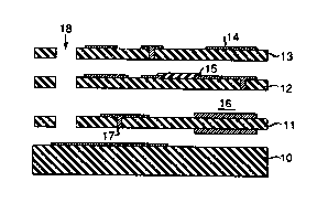
FIG. 1 is an exploded perspective view of a stack of sheets for
fabricating a circuit in accordance with an embodiment of the invention.
' ' ' ' , . j' ' " ' ' ' " , ' " ' ' . ', ' . ' , ., ' '
2 ~ 2 ~
- 2 -
FIG. 2 is a side view of a portion of an apparatus for laminating said
sheets which can be utilized in accordance with the same embodiment, and
FIG. 3 is a schematic view of a further portion of an apparatus for
laminadng said sheets in accordance with the same embodiment.
S It will be appreciated that for purposes of illustration these figures are
not necessarily drawn to scale.
Detai1ed Description
FIG. l shows, for illustrative purposes, a simple multilayer thick film
circuit which could be manufactured in accordance with the invention. The circuit
10 includes several layers of ceramic sheets, 10-13, which are in an unfired or "green"
state. The sheets typically vary in thickness from .1 to .3 mm. Each sheet has two
opposite major surfaces with conductive patterns formed on one or more of the
surfaces. The patterns includes conductors (eg, 14), resistors (lS), and capacitors
(16). Also included are via holes (eg, 17) foITned through the sheets and filled with
15 conductive material to provide interconnection between the components on the
various levels, and a cavity, 18, through sheets, 11-13, for mounting of a
semiconductor chip (not shown). The patterns are formed by standard thick film
techniques such as screen printing using standard materials. For example, the
conductors may be Au, the resistor material Ruthenium based, and the capacitor
20 formed from two conductors on eilher side of a ceramic sheet as shown. The via
holes may be filled by Au. While the patterns are printed on the sheets, the sheets
remain unfired until later in the processing as described below.
- The plurality of sheets are stacked for the purpose of lamination on a
plate such as illustrated in FIG. 2. The plate comprises a base, 20, typically made of
25 Aluminum. The sheets, eg, 21, are aligned on the plate by means of alignment pins,
æ and 23, which extend from the base through holes formed in the sheets. After
stacking, several of such plates may be placed in a rack such as that shown as 30 in
FIG. 3. The rack includes several shelves, eg, 31, upon which the sheets (not shown)
may be mounted in primarily a horizontal orientation. The shelves are coupled by a
30 frame to a cap, 32, which provides a vacuum-tight seal over chamber, 33, within
which the rack is situated. A source, 34, of gas is coupled to chamber, 33, by in1et,
35. Also coupled to the inlet is a pressure gauge, 36, for monitoring the pressure of
the incoming gas. A standard temperature control apparatus, 37, is also coupled to - -
thc chamber through a high presure thermocouple, 38, and heat tape, a portion of
- ,,: . . .: -
: " , :, ~ , . .
,,: "".~,,,"". - , ,, - , ,i ~ ,,, " , ,~
2~3~ 3
which is shown as 39, which is typically a resistor material formed over most of the
surface of the charnber.
The pardcular apparatus employed was a cornmercially available
isostadc pressure equipment sold by Pressure Products Incorporated under the
5 designadon AOH.
In a pardcular example, the sheets were first prelarninated in a standard
uniaxial press such as that sold by Hull under the designation 359-F in order toremove trapped gas between the sheets. This pre-lamination was effected at a lowpresure (less than 70 Kg/cm2) with the sheets heated to a temperature of
10 approximately 70 degrees C for a time of 1 minute. The sheets were then loaded into
the pressure charnber, 33, and air from the gas source, 34, was introduced therein to
create a pressure of approximately 210 Kg/cm2. Preferably, the pressure should be
within the range 150 to 250 Kg/cm . The rack was kept at a temperature of
approximately 70 degrees C, although a range of 50 degrees C to 110 degrees C
15 could be udlized. The isostatic lamination was carried on for approximately 10
minutes although dmes within the range 5 to 15 minutes are generally useful.
Subsequent to the lamination process, the resulting muldlayer parts were
removed from the pressing apparatus and placed in a standard furnace for firing. A
standard burnout of organic material was effected at a temperature of approximately
20 350 degrees C for about 1 hour. This was followed by sintering at a temperature of
approximately 850 degrees C for about 15 minutes. For most ceramic sheets, a
burnout will be performed at 250 to 500 degrees C for 1/2 to 4 hours, and a sintering
at 750 to 950 degrees C for 5 minutes to 2 hours. While the lamination process 5 '
results in a bonding of the various sheets, the firing process fuses the ceramic layers
25 together to form a homogeneous ceramic with the various conductors, resistors, and ~ ~ -
capacitors embedded therein.
It was discovered that the gaseous lamination technique of the present
invendon results in muldiayers with good adherence and apparently no air trappedbetween the layers. Proper registration was also maintained between the layers
30 during the lamination process in spite of the gas flow. As in the liquid isostadc
process, no inserts were needed for defining cavides within the layers, nor was a
canfining die needed to prevent parts from being pressed out of the stack. However,
unlike the liquid process, the present process was done without bagging of the parts.
Various modificadons of the invention will become apparent to those
35 sldllcd in the art. For example, a non-reactive gas such as nitrogen may be employed
a~ ~c gas medium instead of air. Further, although the process is preferably ca~ried
.. . ..
. .
' " '' ,"' ' " :~"' , ','' "' ' ' ',
. .. . . .
2~7~ 3
out without a bag, it might be desirable in certain cases to bag the sheets prior to
laminadon. The bag, however, can be much thinner than that generally needed for
liquid pressing medium (.02 mm thickness), and consequently provide better
conformance to edges and cavity walls. In addition, the pre-lamination step may be
5 unnecessary if the chamber, 33, is first evacuated prior to introduction therein of the
gas from source, 34. All such variations which basically rely on the teachings
through which the invention has advanced the art are properly considered within the
scope of the invention.
,, , , -, , , ,, , ;, , , , : " - :,
' , , ,, ' ' ' ' , ,,: ', " " ' , , ' ,: ',, ," " ' ' ~ '
i , " ,"~, ",, " - ,, , , , , ,,, ;, , ",.. . .. . .
,," , " ,, , ' ' , ' ' ' " ' ' ' ' ':
,. . . ... . .