Note: Descriptions are shown in the official language in which they were submitted.
-
- 202~11g
TWO LAYER MATCHING DIELECTRICS FOR
RADOMES AND LENSES FOR WIDE ANGLES OF INCIDENCE
1 BACKGROUND OF THE INVENTION
1. Technical Field
This invention relates to radomes and lenses and, more
particularly, to a radome or lens with two impedance matching layers.
2. Discussion
Electromagnetic antennas, including radar antennas, are
used under a variety of environmental conditions. Without protection,
these antennas become vulnerable to the adverse effects of rain, heat,
erosion, pressure and other sources of damage, depending upon where the
antenna is used. Radar antennas, for instance, have been used in
space-based, airborne, ship-borne and land-based applications. In each
of these applications an antenna is subjected to a different set of
environmental forces, some of which have the potential to render an
unprotected antenna inoperable or severely damaged.
In order to protect an antenna from the adverse effects of
its environment, antennas have been enclosed by shells which shield the
antenna from its environment. The shielding of the antenna is
typically accomplished by housing it within a relatively thin shell
which is large enough so as not to interfere with any scanning motion
of the antenna. The shielding shells used for radar antennas are
typically called radomes.
A particular radome design is required to protect its
antenna from the surrounding environment, while simultaneously not
1 1 8
1 interfering with signals passed to and from the antenna and while not
interfering with the overall performance of the system upon which the
antenna is mounted. For instance, in airborne applications, a radome
protects an antenna from aerodynamic forces and meteoric damage, while
S at the same time allowing radar transmission and reception, and while
preventing the antenna from upsetting the aerodynamic characteristics
of the airborne vehicle upon which it is mounted. Radomes are employed
in ship-borne applications to protect antennas from wind and water
damage, and from blast pressures from nearby guns.
Lenses have been used in connection with horn antennas to
facilitate transmission and reception of electromagnetic signals. The
lens is typically positioned in the path of the electromagnetic signal,
and in front of the horn antenna. The lens is used to bend or focus
the signal, as the signal is transmitted or received.
Of particular importance are the electromagnetic charac-
teristics of materials used in building the radome or lens. Currently,
the structures used to produce radomes and lenses possess permit-
tivities that are not equal to that of free space or of the atmosphere.
The resulting impedance mismatch can cause reflections at the
boundaries of the radome or lens, and can cause distortion and loss in
the electromagnetic signal. The adverse consequences of an impedance
mismatch become particularly acute when electromagnetic signals are
transmitted or received from high angles of incidence with respect to
the radome or lens. Attempts have been made in the past to minimize
the effects of the impedance mismatch between the atmosphere or the
free space that is in contact with the radome or the lens. For
instance, prior attempts to match a radome or lens with a permittivity
of:
~radome or lens = 4 ~o
(~0 being the permittivity of free space) have included a single
impedance matching layer between the radome or lens and the atmosphere.
This impedance matching layer has typically had a permittivity whose
value falls between that of the atmosphere or free space, and the
2024 1 1 8
radome or lens. These previous impedance matching designs have shown
good performance only when inco~ing electromagnetic signals have had
small angles of Lncidence. These prior designs have also shown
significant sensitivity to signal polarization.
SUMMARY OF THE ~NV~NlION
The present invention provides an impedance matching design
for a structure, such as a lens or radome, and its surrounding
environment. The design employs two (2) impedance matching layers.
The present invention provides an optimized transmission characteristic
that exhibits minimal polarization sensitivity. In the preferred
embodiment, a radome or lens with a permittivity greater than that of
free space is matched to its surrounding environment through the use of
two (2) optimized impedance matching layers.
Other aapectc of thic invention are aa followa:
A multi-layered ~tructure having a ba~e or ~Up~GL L member for
receiving and pa~aing incident elect~ -gnstic energy to and from
an adjacent ambient dielectric medium, said multi-layered structure
comprising:
a first i o~Ance matching layer in contact with said
adjacent ambient dielectric medium, said fir~t i a~nce matching
layer having a permittivity higher than that of said adjacent
ambient dielectric medium;
a eecond ~ an~e matching layer in contact with ~aid firet
i ---nre matching layer, said second i ed~nce matching layer
having a permittLvity higher than that of oaid first i ~'-nc-
matching layer, wherein caid pormittivity of eaid eecond ; _~Ance
matching layer io greater than a square root of ~aid permittivity
of said eupport or bace member, and, wherein ~aid permittivity of
eaid fir~t ; -'-nco matching layer divided by eaid permittivity of
~aid ~econd ~_a'-nce matching layer ie equal to the equare root of
said permittivity of ~aid adjacent ambient dielectric medium
divided by the cquare root of eaid permittivity of said eupport or
base member, wherein said permittivity of said ~econd ; ia'Ance
matching layer i~ 3 times the permittivity of ~aid ad~acent ambient
dielectric medium, (3 * ~o)~ wherein said permittivity of said
fir~t ; _~nce matching layer i8 1. 5 time~ the permittivity of
said adjacent ambient dielectric medium ~1.5 * ~O)~ wherein ~aid
20241 18
_ 3a
~econd i r~_~Ance matching layer has a thickne~s of 0 833
centimeters ~cm), and wherein said first i pe~Ance matching layer
has a thickness of 1 441 centimeters (cm);
said support or base member being in contact with aaid second
; _3'Ance matching layer, ~aid base member having permittivity
higher than that of ~aid second i~ E~ance matching layer wherein
said permittivity of said support or base member is 4 time~ (*) the
permittivity of ~aid adjacent ambient dielectric mediu~7 (4 * ~o);
and
said multi-layered structure providing a substantially
optimized transmis~ion bandwidth for both transver~e electric and
transverse magnetic polarization~ of said elect~ -g~tic energy
for wide angle~ of incidence
A radome for receiving and pa~oing incident elect~. -qn~tic
energy to and from an adjacent am~7ient dielectric medLum, said
radome comprising
a first i _dA~ce matching layer in contact with said
adjacent ambient dielectric medium, said first i ,~'Ance matching
layer having a permittivity higher than that of said ad~acent
ambient dielectric medium;
a second ~ nce matching layer in contact with ~aid first
i ~rc'-ncs matching layer, said second i -~nce matching layer
having a permittivity higher than that of ~aid first i~ -'An~e
matching layer, wh-rein the permittivity of ~aid ~econd i ~a'An~Q
matching layer i~ 3 time~ the permittivity of said adjacent ambient
dielectric medium, (3 * rO) and wherein the permittivity of the
fir~t i rc'~nre matching layer is 1 5 times the permittivity of
said adjacent ambient dielectric medium (1 5 * rO);
a shell in contact with said second ; L c~Ance matching layer,
said shell having a permittivity higher than that of said second
i ~'An~e matching layer, wherein said permittivity of ~aid oecond
; r~='Ance matching layer is greater than the square root of said
permittivity of said shell, and wherein said permittivity of said
firot ; 3~Ance matching layer divided by said permittivity of said
- second ; ~Ance matching layer is equal to the square root of said
permittivity of said adjacent ambient dielectric medium divided by
the square root of ~aid permittivity of said shell, and wherein
~aid permittivity of ~aid shell is 4 time~ (*) the permittivity of
- said adjacent ambient dielectric medium, ~4 * ~0);
~ aid two i ~ nce matching layer~ cooperating with ~aid
~h-ll to provid- a ~ub~tantially optimized tran~mis~ion bandwidth
for both tran~ver~e electric and tran~ver~e magnetic polarization~
of ~aid electromagnetic energy for angles of incidence of 0 to 60
de~e-~;
" ~`
3b 2024 1 1 8
a third ; ~Ance matching layer in contact with said shell,
said third layer being in contact with the surface of ~aid shell
oppoaite to the ~urface of Qaid ~hell that is in contact with said
sQcond layer, ~aid third layer having a permittivity equal to ~aid
permittivity of said second layer;
a fourth i ~'Ance matching layer in contact with said third
layer on one ~ide and in contact with said adjacent ambient
dielectric medium on the other side, said fourth layer having a
permittivity equal to said permittivity of oaid first layer; and
wherein ~aid ~econd and ~aid third i s~n~e matching layer- have a
thickne~ of 0 833 centimeter~ (cm), and, wherein said fir~t and
~aid fourth ; ~ ncs matching layer~ have a thicknes~ of 1,441
centimeter- ~cm)s and
~ aid four i a'-nce matching layer~ cooperating with said
~hell to provide a ~ub~tantially opt~ i~ed tran~miasion bandwidth
for both tran-ver-e electric and tran-ver-e magnetic polarization~
of ~aid elect~ -gn~tic energy for angle~ of incidence of 0 to 60
de~Lee~
A focusing device for receiving and passing incident
electc~ ~gn~tic energy to and from an adjacent ambient dielectric
medium, said focu~ing device comprising
a first i r,3dAnce matching layer in contact with said
adjacent ambient dielectric medium, said first ; 2'Ance matching
layer having a permittivity higher than that of said adjacent
ambient dielectric medium;
a ~econd ~ a~Ance matching layer in contact with ~aid fir~t
; ~- nc~ matching layer, aid econd i e~Ance matching layer
having a permittivity higher than that of said fir~t ; -'~ncs
matching layer wherein ~aid permittivity of ~aid second ; a'-nce
matching layer is 3 time- the permittivity of said ad;acent ambient
dielectric medium, ~3 * ~0), and, wherein ~aid permittivity of ~aid
first ; ~2'~nce matching layer is 1 5 times the permittivity of
said adjacent ambient dielectric medium (1 5 ~0);
a len~ in contact with said second ; ~Ance matching layer,
~aid lens having a permittivity higher than that of ~aid second
; e~A~ce matching layer wherein the permittivity of said lens is 4
timeo (*) the permittivity of oaid adjacent ambient dielectric
medium, (4 * ~0), wherein said permittivity of said second
; r,a'~nce matching layer is greater than the square root of said
permittivity of ~aid len~, and wherein ~aid permittivity of oaid
~econd ; r,~-n~e matching layer is equal to the ~quare root of oaid
permittivity of ~aid adjacent ambient dielectric medium divided by
the quare root of ~aid permittivity of oaid leno;
2024 1 1 8
3c
~ aid two ~ nce matching layer~ cooperating with said len~
to provide a substantially optimized transmission bandwidth for
both transverse electric and transver~e magnetic polarization~ of
said electr~ -7nstic energy for angle~ of incidence of O to 60
degrees;
a third i _c'Ance matching layers in contact with said lens,
said third layer being in contact with the surface of said lens
opposite to the surface of said lens that is in contact with said
second layer, said third layer having a permittivity equal to said
permittivity of said second layer;
a fourth ; ~Ance matching layer in contact with said third
layer on one side and in contact with said ad;acent ambient
dielectric medium on the other side, said fourth layer having a
permittivity equal to said permittivity of said first layer,
wherein said second and said third i r~ nee matching layers have a
thickne~- of 0 833 centimeter~ (cm), and wherein oaid first and
~aid fourth ; ~.~anc- matching layer~ have a thic~n~ of 1,441
c~ntimet~re (cm); and
~ id four ~ p~'~nce matching layers cooperating wlth ~aid
lens to provide a substantially optimized tran~ ission bandwidth
for both transverse electric and transverse magnetic polarizations
of said elect~ -gn~tic energy for angles of incidence of O to 60
degrees
BRIEF DESCRIPTION OF THE DRAWINGS
The various ob~ects snd advantages of the present invention
will become apparent to those skilled in the art by reading the
following specification and by reference to the drawings in which
FIG 1 is a ray tracing through four (4) dielectrics of
increasing permittivity;
FIG 2 is a graph illustrating the transmission
characteristics of electromagnetic energy in the transverse magnetic
polarization for a structure having two (2) optimized impedance
matching layers for an incident angle of sixty degrees (60);
FIG 3 is a graph illustrating the transmission
characteristics of electromagnetic energy in the transverse electric
polarization for a structure having the same two (2) optimized
impedance matching layer~ as in FIG 2 for an incident angle of sixty
degrees (60);
FIG 4 is a graph illustrating the transmission
characteristics of electromagnetic energy in the transverse magnetic
polarization for a structure having the same two (2) optimized
2024 1 1 8
l impedance matching layers as in FIG. 2 for an incident angle of fifty
degrees (50);
FIG. 5 is a graph illustrating the transmission
characteristics of electromagnetic energy in the transverse electric
polarization for a structure having the same two (2) optimized
impedance matching layers as in FIG. 2 for an incident angle of fifty
degrees (50);
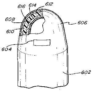
F~G. 6 is a view showing a radome made in accordance
with the teachi n~e of this invention, the radome being mounted on
an airborne vehicle; and
FIG. 7 is a view ehowing a focusing device made in
accordance with the teachings of this invention, the focucing
device being ueed to bend incoming and outgoing elect~ netiC
signale in conncction with a horn antenna.
DESCRIPTION OF THE PREFERRED EMBODIMENT
With reference now to the drawings, and more particularly
to FIG. l, there is shown a support or base member 2 with impedance
matching layers 4 and 6, in contact with an adjacent ambient dielectric
medium 8, such as air or free space. The permittivity of support or
base member 2 is ~3, which is greater than the permittivity of impedance
matching layer 4. The permittivity of impedance matching layer 4 is ~2.
which is greater than the permittivity of impedance matching layer 6.
The permittivity of impedance matching layer 6 is ~" which is greater
than the permittivity of adjacent ambient dielectric medium 8. The
permittivity of ad~acent ambient dielectric medium 8 is ~0, which is
typically equal to the permittivity of the atmosphere or of free space.
Incident ray l0 travels through the ad~acent ambient dielectric medium
8, and represents the path of an electromagnetic signal that is being
received by support or base member 2 from medium 8. However, the path
of ray l0 could also represent an electromagnetic signal that is being
transmitted from base member 2 to medium 8. Ray l0 creates an angle of
incidence 90, with respect to the normal 12 of the boundary between
impedance matching layer 6 and ad~acent ambient dielectric medium 8.
i~ ~
202~18
.
1 As is known in the art, as ray 10 travels across the
boundary between adjacent ambient dielectric medium 8 and impedance
matching layer 6, ray 10 will be refracted or bent in accordance with
Snell's law. Therefore, because impedance matching layer 6 has a
permittivity greater than that of adjacent ambient dielectric medium 8,
angle ~ will be less than the angle of incidence ~0. As ray 10 crosses
the boundary between impedance matching layer 6 and impedance matching
layer 4, it will again be refracted according to Snell's law. Ray 10
creates angle ~, with respect to normal 14 of the boundary between
impedance matching layer 4 and impedance matching layer 6. Because the
permittivity of impedance matching layer 4 is greater than that of
impedance matching layer 6, angle ~2 will be less than angle ~,.
Similarly, as ray 10 crosses the boundary between impedance matching
layer 4 and support or base member 2, it will again be refracted
according to Snell's law. Because the permittivity of support or base
member 2 is greater than that of impedance matching layer 4, angle 93
with respect to the normal 16 of the boundary between impedance match-
ing layer 4 and support or base member 2, will be less than angle 92.
In a particularly useful (but not limiting) embodiment, the
thickness X, of impedance matching layer 6 is 1.441 centimeters (cm) and
the thickness X2 of impedance matching layer 4 is 0.833 centimeters (cm)
so that the layers 6 and 4 are tuned for an electromagnetic signal of
frequency 6 GHz, as is shown in FIG. 1. As illustrated in FIG. 1, the
permittivity ~3 of support or base member 2 is four (4) times that of
the permittivity ~0 of ad;acent ambient dielectric medium 8 (4 * ~0).
Based on this permittivity for support or base member 2, the optimal
permittivity ~2 for impedance matching layer 4 is three (3) times the
permittivity of adjacent ambient dielectric medium 8 (3 * ~0).
Similarly, the optimal permittivity ~, for impedance matching layer 6
is 1.5 times the permittivity of adjacent ambient dielectric medium 8
(1.5 * ~0). It will be readily apparent to those skilled in the art
that thickness X2 of impedance matching layer 4 and thickness X, of
impedance matching layer 6 can be altered to tune these impedance
matching layers for incident electromagnetic signals with frequencies
other than 6 GHz. Similarly, the optimal transmission characteristics
for both transverse magnetic and transverse electric polarizations of
2~:4II8
1 electromagnetic signals to or from an adjacent ambient dielectric
medium 8 with permittivity ~0 can be achieved for a support or base
member 2 with a given permittivity ~3 by using the following relation-
ships for the permittivity ~2 of matching layer 4 and the permittivity
~, of matching layer 6:
~0 = permittivi~ of free space or air;
2 = ~ ~ 3;
~3 S ~2 S ~3;
lo for ~0 s ~3;
for angles of incidence 0 s ~0 s 60; for electromagnetic signals
ranging from microwave to optical frequencies; and for a 60Z transmis-
sion bandwidth around the tuning frequency.
While FIG. 1 illustrates an embodiment of the present
invention that has a planar or flat shape, it should be understood that
the present invention can be effectively embodied in a curved multi-
layered structure, such as a curved radome or lens. A curved radome or
lens will realize the present invention's advantages provided that the
curvature of the radome or lens is "electrically large" with respect to
the incident or transmitted electromagnetic signals. As is known in
the art, a curved multi-layered structure is electrically large with
respect to a given signal if the radius of curvature of the multi-
layered structure is significantly larger than the wavelength of the
given electromagnetic signal. As is known in the art, when a multi-
layered structure is electrically large the multi-layered structure
may be locally approximated as a planar or flat multi-layered structure
as illustrated in FIG. 1.
Turning now to FIG. 2, there is shown the transmission
characteristics of a multi-layered structure comprised of a support or
base member with two (2) optimized impedance matching layers, like that
of FIG. 1, for electromagnetic signals in the transverse magnetic
polarization. Transmission in decibels is plotted along axis 202 as a
function of signal frequency in GHz plotted along axis 204. Curve 206
2~24:~8
1 illustrates the transmission characteristic for a range of signal
frequencies near 6 GHz, and for an electromagnetic signal passing to or
from adjacent ambient dielectric medium 8 at an angle of incidence ~0
of sixty degrees (60) upon impedance matching layer 6. The transmis-
sion characteristic of FIG. 2 illustrates the situation where thethicknesses X, and X2, and the permittivities of impedance matching
layers 6 and 4, the permittivity of the support or base member 2, and
the permittivity of the ad;acent ambient dielectric medium 8 are all
equal to those illustrated in FIG. 1.
Turning to FIG. 3, there is shown the transmission
characteristics of a multi-layered structure comprised of a support or
base member with two (2) optimized impedance matching layers, like that
of FIG. 1, for electromagnetic signals in the transverse electric
polarization. Transmission in decibels is plotted along axis 302 as a
function of signal frequency in GHz plotted along axis 304 for the same
surface used to generate the characteristic of FIG. 2. Curve 306
illustrates the transmission characteristic for a range of signal
frequencies near 6 GHz, and for an electromagnetic signal passing to or
from adjacent ambient dielectric medium 8 at an angle of incidence ~0
of sixty degrees (60) upon impedance matching layer 6. The transmis-
sion characteristic of FIG. 3 illustrates the situation where the
thicknesses X, and X2, and the permittivities of impedance matching
layers 6 and 4, the permittivity of the support or base member 2, and
the permittivity of the ad;acent ambient dielectric medium 8 are all
equal to those illustrated in FIG. 1.
Turning to FIG. 4, there is shown the transmission
characteristics of a multi-layered structure comprised of a support or
base member with two (2) optimized impedance matching layers, like that
of FIG. 1, for electromagnetic signals in the transverse magnetic
polarization. Transmission in decibels is plotted along axis 402 as a
function of signal frequency in GHz plotted along axis 404 for the same
surface used to generate the characteristic of FIG. 2. Curve 406
illustrates the transmission characteristic for a range of signal
frequencies near 6 GHz, and for an electromagnetic signal passing to or
from adjacent ambient dielectric medium 8 at an angle of incidence ~0
of fifty degrees (50) upon impedance matching layer 6. The transmis-
8 2024 1 1 8
l sion characteristic of FIG. 4 illustrates the situation where thethicknesses X, and X~, and the permittivities of impedance matching
layers 6 and 4, the permittivity of the support or base member 2, and
the permittivity of the ad~acent ambient dielectric medium 8 are all
equal to those illustrated in FIG. 1.
Turning now to FIG. 5, there is shown the transmission
characteristics of a multi-layered structure comprised of a support or
base member with two (2) optimized impedance matching layers, like that
of FIG. 1, for electromagnetic signals in the transverse electric
polarization. Transmission in decibels is plotted along axis 502 as a
function of signal frequency in GHz plotted along axis 504 for the same
surface used to generate the characteristic of FIG. 2. Curve 506
illustrates the transmission characteristic for a range of signal
frequencies near 6 GHz, and for an electromagnetic signal passing to or
from ad~acent ambient dielectric medium 8 at an angle of incidence ~0
of fifty degrees (50-) upon impedance matching layer 6. Similarly, the
transmission characteristic of FIG. 5 illustrates the situation where
the thicknesses X, and X2, and the permittivities of impedance matching
layers 6 and 4, the permittivity of the support or base member 2, and
the permittivity of the ad~acent ambient dielectric medium 8 are all
equal to those illustrated in FIG. 1.
Turning now to FIGS. 6 and 7, there is illustrated
two (2) viewe of ~ ' ~ d; - - ts mado in accordanco with the
te~ch~ngs of this invention. FIG. 6 illustrates the use of a radome
made in accordance with the te~ g~ of the present invention in
connection with an airborne vehicle 602. Radar antenna 604 is housed
within the radome. Radome 606 is shown as having a cut away portion,
exposing the layers of the structure that are ueod to create radom~ 606.
Layer 608 is a first impedance matching layer substantially identical
to layer 6 in FIG. 1. Layer 610 is an impedance matching layer
substantially identical to layer 4 in FIG. 1. Shell 612 is a base
member substantially identical to base member 2 in FIG. l. Layer 614
is an impedance matching layer substantially identical to layer 4 in
FIG. 1. Similarly, layer 616 is an impedance matching layer substan-
tially identical to layer 6 in FIG. 1. In the typical radome, both
sides of a shell 612 must be matched to its surrounding environment
2021118
-
1 because there is typically an atmosphere or free space in contact with
both sides of the shell. Because both sides of a given shell must pass
electromagnetic energy to and from an adjacent ambient dielectric
medium, the typical radome made in accordance with the present
invention will use two (2) impedance matching layers on each side of a
given shell.
FIG. 7 illustrates the use of a focusing device 706 made in
accordance with the teachings of the present invention in connection
with a horn antenna 702. Focusing device 706 is shown as being
comprised of four (4) impedance matching layers 710, 712, 716 and 718
and lens 714. Layer 710 is an impedance matching layer substantially
identical to layer 6 in FIG. 1. Layer 712 is an impedance matching
layer substantially identical to layer 4 in FIG. 1. Layer 716 is an
impedance matching layer substantially identical to layer 4 in FIG. 1.
Similarly, layer 718 is an impedance matching layer substantially
identical to layer 6 in FIG. 1. Lens 714 is a base member substan-
tially identical to base member 2 in FIG. 1. Without impedance
matching layers 710, 712, 716 and 718, both sides of lens 714 would be
in contact with the adjacent ambient dielectric medium such as air or
free space in the surrounding environment. In order to match the
permittivity of lens 714 with its surrounding environment, focusing
device 706 is made in accordance with the present invention and
includes two (2) impedance matching layers on each side of lens 714.
A substantially planar wave 708 is shown as being incident
on lens 706. Wave 708 is bent by lens 706 as it passes through the
lens. A substantially spherical wave 704 is transmitted from lens 706
to horn antenna 702. Typically, horn antenna 702 can transmit as well
as receive electromagnetic signals. FIG. 7 illustrates transmission as
well as reception. When transmitting, horn antenna 702 emits a
substantially spherical wave 704. Wave 704 is incident upon lens 706.
Lens 706 bends wave 704 and transmits a substantially planar wave 708.
It should be understood that while this invention was
described in connection with one particular example, that other
modifications will become apparent to those skilled in the art after
having the benefit of studying the specification, drawings and
following claims.