Note: Descriptions are shown in the official language in which they were submitted.
2-02~385
20982-EPC/RDS -1-
PRBDI~-~ OK'~ ~ FOR T~TN~ T ZATION
OF BLBCTRONIC AND OPTICAL SIGNALS
Field of the Invention
This invention relates to an electronic circuit
for providing a linear output from an amplitude
modulated transmission device such as a semiconductor
laser which has an output distorted from its input due
to inherent nonlinearity. The distortion of the
nonlinear device is compensated by applying a
predistorted signal to the input of the nonlinear
device. The predistortion is chosen such that the
distortion of the nonlinear device restores the
undistorted signal.
2 5 Back~round of the Invention
Directly modulating the analog intensity of a
light-emitting diode (LED) or semiconductor laser with
an electrical signal is considered among the simplest
methods known in the art for transmitting analog
signals, such as sound and video signals, on optical
fibers. Although such analog techniques have the
advantage of significantly smaller bandwidth
requirements than digital pulse code modulation, or
analog or pulse frequency modulation, amplitude
modulation may suffer from noise and nonlinearity of
the optical source.
*
-2- 202~38~
1 Distortion inherent in certain analog transmitters
prevents a linear electrical modulation signal from
being converted linearly to an optical signal, and
instead causes the signal to become distorted. These
effects are particularly detrimental to multi-channel
video transmission which requires excellent linearity
to prevent channels from interfering with each other.
A highly linearized analog optical system has wide
application in commercial TV transmission, CATV,
interactive TV, and video telephone transmission.
Linearization of optical and other nonlinear
transmitters has been studied for some time, but
proposed solutions suffer from practical disadvantages.
Most applications have bandwidths which are too large
for practical use. Feedforward techniques require
complex system components such as optical power
combiners and multiple optical sources. Quasi-optical
feedforward techniques suffer from similar complexity
problems and further require extremely well-matched
parts.
One method employed in the past to reduce
distortion inherent in nonlinear devices has been
predistortion. In this technique, a modulation signal
is combined with a signal equal in magnitude to the
distortion inherent in the nonlinear device but
opposite in sign. When the nonlinear device modulates
the combined signal, the device's inherent distortion
is canceled by the combined signal's predistortion and
only the linear part of the source signal is
transmitted. This predistortion signal is usually in
the form of additive and subtractive combinations of
the input fundamental frequencies as these
intermodulation products constitute the most fertile
source of distortion in analog signal transmission. In
the distribution of AM signals for cable television,
for example, there are often as many as 40 frequencies
on a particular band and plenty of opportunities for
~ _3_ 202~38S
1 second order and third order intermodulation products
of those frequencies.
Current predistortion techniques generally divide
an input signal into two or more electrical paths and
generate predistortion on one or more of the paths
resembling the distortion inherent in the nonlinear
transmitting device. The generated predistortion is
the inverse of the nonlinear device's inherent
distortion and serves to cancel the effect of the
device's inherent distortion when recombined with the
input signal.
Attenuation can be used to match the magnitude of
the predistortion to the magnitude of the device's
inherent distortion characteristics before the signals
are recombined and sent to the nonlinear device for
modulation. However, the method suffers from crudeness
because nonlinear devices frequently have amplitude and
phase distortion characteristics dependent on the
frequency of the modulating signal. Present techniques
provide no means for compensating for these
frequency-dependent nonlinearities.
Neglecting to correct for the frequency dependence
of the distortion leads to a result which may be quite
tolerable for many systems and for signals with
relatively narrow bandwidth. However, they become
particularly troublesome when converting an electrical
TV signal to an optical signal for cable transmission.
Such signals for cable TV may have forty or more input
frequencies, all of which need to have high quality
amplitude modulated signals. The transmission devices
for such signal must have an exceptionally high degree
of linearity.
The present invention accordingly is addressed to
these and other difficulties found in the prior art.
-4- 202438S
1 8ummary of the Invention
Thus, in practice of this invention according to
a presently preferred embodiment, a predistortion
circuit for reducing distortion in the transmission of
analog signals splits an input modulation signal into
two electrical paths, one primary and one secondary.
A predistortion amplifier on the secondary path
generates second order or higher order intermodulation
distortion products of the input signal. The
distortion so generated, or predistortion, is adjusted
to be substantially equal in magnitude and opposite in
sign to the distortion inherent in a nonlinear
modulation device to which the signal is applied. The
predistortion signal is adjusted in amplitude and phase
to match the frequency dependence of the distortion by
the nonlinear device. The phase of the signals are
synchronized by a delay or phase adjustment element in
one of the electrical paths. The primary and secondary
signals are then recombined to produce a single
modulation signal including intermodulation product
distortion. Thus, the predistortion circuit largely
linearizes the transmission of modulating signals by
cancelling distortion inherent in nonlinear
transmitting devices.
_ ~5~ 2~ ~3~
1 Brief Description of the Drawing~
These and other features and advantages of this
invention will be better understood and more fully
appreciated by reference to the following detailed
description when considered in conjunction with the
accompanying drawings, wherein:
FIG. 1 is a block diagram showing a presently
preferred embodiment of a predistortion circuit;
FIG. 2 is a block diagram of a push-push amplifier
employed in the predistortion circuit according to a
preferred embodiment of this invention;
FIG. 3 is a schematic diagram exemplifying a
practical predistortion circuit; and
FIG. 4 is an illustration of the effect of
predistortion on the waveforms of a modulation signal.
-6- 202~38~
1 Detailed Description
The concept of predistortion is shown abstractly
in FIG. 4. An input signal Y0 is input to a
predistortion network 40. The predistortion network
has a nonlinear transfer function which deviates from
linearity oppositely and inversely from the deviation
of a nonlinear transmitter having a known transfer
function 41. The signal Y1 from the predistortion
network is a combination of the input source signal Y0
and predistortion resulting from the nonlinear transfer
function 40. Signal Y1 is fed into the nonlinear
transmitter and, after modulation by the transmitter,
appears as a substantially linear signal Y2 as a result
of the inherent distortion of the transmitter inversely
related to and cancelled by the predistortion of signal
Y1 -
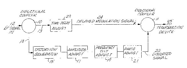
Referring now to FIG. 1, an input source signal 12
feeds into a directional coupler 10 and is split into
a primary electrical path 13 and a secondary electrical
path 14. Typically, the portion of the signal on the
primary electrical path is substantially larger in
power than the signal on the secondary electrical path.
For example, an 11 dB directional coupler may be used
to achieve this result.
The secondary electrical path comprises in circuit
series a distortion generator 15, an amplitude
adjustment block 17, a "tilt" or frequency adjustment
block 19, and a fine phase adjustment block 21. These
elements may be varied in order along the secondary
electrical path without departing from the functional
purpose of the invention.
In one embodiment, the signal on the secondary
electrical path feeds first into the distortion
generator. The output of the distortion generator
comprises intermodulation distortion of the input
frequencies. Second order or second and higher order
distortion may be produced. Ideally, the fundamental
~- 202438~
--7--
1 frequency is suppressed in the distortion generator by
cancellation, filtering or other means. The
intermodulation product so generated is opposite in
phase to the input signal. This inversion may be
accomplished within the distortion generator or with a
separate inverter element (not shown).
The distorted output from the distortion generator
is matched in magnitude to the magnitude of inherent
distortion predicted in the transmission device (not
shown in Fig. 1) receiving the output signal 25. The
matching function occurs in the amplitude adjustment
block 17 and this adjustment may be accomplished
manually with a variable attenuator or dynamically with
an automatic gain control element, for example. The
output of the amplitude adjustment block 17, therefore,
comprises intermodulation distortion of a small portion
of the input signal and is substantially equal in
magnitude and opposite in sign to distortion inherent
in a nonlinear transmission device receiving the output
signal 25 of the predistortion circuit. This output or
predistortion signal effectively reduces the frequency
independent component of the distortion of the
nonlinear device.
Generation of the predistortion signal on the
secondary electrical path typically involves a time
delay relative to the primary electrical path. Before
the primary and secondary paths are recombined an
adjustment is made to set the relative phase of the
primary path electrical signal with respect to the
phase of the secondary path electrical signal which
results in best cancellation of the distortion inherent
in the nonlinear device. This phase matching is done
on the primary electrical path by an external delay 23
which receives the primary portion of the signal 13
split by the directional coupler 10. The time delay
may be manually or automatically adjusted. An
~ -8- ~a~
1 exemplary delay may be simply a transmission line of
selected length to introduce a suitable delay.
An exemplary transmission device may be a semicon-
ductor laser or LED modulated by the output signal.
The inherent distortion of such a device is not
independent of frequency. Generally speaking, the
distortion is inherently greater at higher frequencies.
To adjust for frequency dependent distortion of
the nonlinear transmitting device, the output of the
amplitude adjustment block is then fed into a frequency
adjustment or "tilt" adjustment block 19. The tilt
adjustment is a variable filter or other similar means
which increases the amplitude of the distortion at high
frequencies for an "up-tilt" and decreases it at high
frequencies for a "down-tilt." This adjustment, like
the amplitude adjustment, may be done either manually
or automatically. By passing more or less of the
high-frequency distortion products than the
low-frequency distortion products, the tilt adjustment
enables the predistortion signal to be tailored more
precisely to the inherent distortion characteristics of
the nonlinear device.
Typically, the amplitude adjustment is made to
compensate for the distortion occurring at the low
frequency end of the band. The frequency adjustment is
then made as an up-tilt to compensate for distortion at
the high frequency end of the band. It may be noted
that this same effect can be achieved by amplitude
adjustment at the high frequency end, and an up-tilt or
down-tilt on the low-frequency end as an appropriate
attenuation or amplification of the signal.
An additional fine phase adjustment block 21 on
the secondary electrical path provides for more
accurate setting of the relative phase between the
distortion generated in the secondary path and the
distortion inherent in the nonlinear device. This
adjustment, like the amplitude adjustment, may also be
- 9 20~438~
1 made manually and may be frequency dependent. It is
found that manual adjustment of amplitude, frequency
and phase is usually completed in less than a minute.
What one does is make the appropriate adjustment while
observing the distortion in the output of the nonlinear
device. The adjustment seeks to minimize the final
distortion. The optimum adjustment is when the
predistortion signal is of the same magnitude as the
distortion inherent in the nonlinear device, and the
predistortion is exactly 180 out of phase with the
distortion.
It is significant that the phase adjustment is
made relative to the distortion of the device.
Previously time delays have been introduced so that the
predistortion is exactly in phase (or 180 out of
phase) with the primary signal. This may be sufficient
for some purposes, but is not suitable for others, such
as TV bandwidth modulation of a laser, for example.
Once the relative phases of the signals on the
primary and secondary electrical paths have been set,
they are recombined by the output directional coupler
11. The combined signal 25, including the
predistortion component from the secondary path, is
output to a nonlinear transmission device for
modulation of the signal.
An example of a predistorter or distortion
amplifier block 15 is shown in detail in FIG. 2. A
portion of the input signal 14 on the secondary
electrical path is fed into a 180 splitter 30 which
divides the signal into a first electrical path 58 and
a second electrical path 39 of equal magnitude and
opposite sign. If desired, the signals so divided need
not be of equal magnitude if subsequently amplified or
attenuated.
The first electrical path feeds into a first
amplifier 32 generating second order and higher order
intermodulation products of the fundamental frequencies
-lO- 2024~85
1 in the input signal 14. The second electrical path,
carrying a signal opposite in sign to the first
electrical path, feeds into a second amplifier 33
generating even order intermodulation products which
are of the same sign as those output by the first
amplifier 32, but generating odd order intermodulation
products opposite in sign to those output by the first
amplifier. The signals are combined additively by a
O-degree combiner 34 which substantially reduces the
fundamental frequencies and odd order intermodulation
products, leaving even order intermodulation product
components in an output signal 37. Ideally, this
process produces pure second order and higher order
even components of intermodulation distortion.
The first and second amplifiers 32 and 33 are
adjustable to prevent complete cancellation of the odd
order intermodulation product components. This
adjustment can be accomplished by varying the bias
currents to the amplifiers which has little effect on
gain of the fundamental frequencies. An increase in
the bias current of the first amplifier 32 with a
corresponding decrease in the bias current of the
second amplifier 33 will unbalance the two amplifiers
in the sense that the magnitude of intermodulation
products produced will no longer be identical between
the two amplifiers. Thus, the odd order
intermodulation products will not cancel one another.
The unbalancing of this distortion circuit, which
is referred to as a push-push amplifier, allows
generation of intermodulation distortion of all orders
of interest for predistortion purposes. The
fundamental frequencies may be suppressed by particular
amplifier design or by filtering means (not shown)
either in series with, after or integral to each
amplifier. Preferably, the bias currents of both
amplifiers 32 and 33 are adjusted in equal and opposite
directions or senses, so that the unbalance affects
- 20213~5
--11--
1 only the odd order intermodulation products and the
even order intermodulation products remain balanced and
substantially unchanged in magnitude.
One embodiment of the predistortion circuit is
shown in FIG. 3. The signal 14 in the secondary path
from the signal splitting coupler 10 is first
attenuated by way of an adjustable attenuator R1, R3 to
assure a constant signal level. If the signal is too
small there may not be sufficient distortion to
compensate for the distortion of the transmission
device. Conversely, if the signal is too large, the
distorter could be overloaded and itself produce
unacceptable distortion.
The attenuated signal is split in the 180
splitter 30, and capacitively coupled to the first and
second amplifiers 32 and 33. The bias of the
amplifiers is adjusted to obtain the desired third
order and higher order intermodulation products, and
the recombined signal is attenuated by way of the
amplitude adjustment 17 to obtain the desired amount of
distortion at relatively low frequencies, such as 50
MHz. Next one checks the higher frequency end of the
band and adjusts the frequency filter 19 until the
distortion matches the inherent distortion of the
transmission device at this higher frequency. This has
little effect on the predistortion at the lower
frequency end of the band. It, in effect, tilts the
amplitude as a function of frequency around a pivot
near the low end of the band.
The time delay 23 is adjusted at the high
frequency end of the band to adjust the phase of the
signal in the primary signal path. Again, this has
little effect at the low frequency end of the band.
Finally, the phase adjustment 21 is used to more
precisely adjust the phase of the predistortion
generated in the secondary path to compensate for the
phase distortion by the nonlinear device. If need be,
202~385
-12-
1 the adjustment sequence can be repeated to more closely
match the inherent distortion of the transmission
device. Ordinarily, the initial attenuator and the
bias of the predistortion amplifiers need not be
adjusted, but may remain in a preset state. The three
adjustments of the amplitude, tilt, and phase are
sufficient. The principal delay in the primary path
may also be fixed for a given secondary path.
The signal in the secondary path is recombined
with the signal in the primary path by way of the
directional coupler 11, and the signal 25 thereby
predistorted is applied to a laser 38 or the like for
modulation.
Many variations and modifications will be apparent
to those skilled in the art without departing from the
spirit and scope of the invention. For example,
although described and illustrated in the context of a
TV signal modulating a laser or light emitting diode,
other nonlinear devices such as amplifiers may have
inherent distortion largely cancelled by this
technique. The fine adjustment of the relative phase
of the signals in the primary and secondary paths is in
the secondary path in the illustrated embodiment, but
this could also be in the primary path with the coarse
adjustment. The secondary path is preferred since such
a delay in the primary path may have an inappropriate
impedance for this path.
In this embodiment, there is a single secondary
signal path with its distortion generator. If desired,
a third "secondary" path could be employed with one
path generating second order cancellations signals and
another path generating third order cancellation
signals. Each of these paths may have its own
adjustment for frequency dependence of amplitude and
phase. In such an embodiment it is preferred to have
fine adjustment of phase in each of the secondary
paths. In the event two or more secondary paths are
2024385
-13-
1 used for higher order distortion, the amplitude, tilt
and phase in either path may be adjusted first since
there is no interaction between them.
Because of such variations, the invention may be
practiced other than as specifically described.