Note: Descriptions are shown in the official language in which they were submitted.
292~588
SWITCHING REGULATOR OF A SIMPLE STRUCTURE
CAPABLE OF REDUCING A SWITCHING LOSS
Background of the Invention:
This invention relates to a switching regulator
for use in regulating an input a.c. voltage into an
output d.c. voltage.
A conventional switching regulator of the type
described comprises a rectifying circuit supplied with
an input d.c. voltage to produce a rectified voltage and
a converter circuit for converting the rectified voltage
into an output d.c. voltage. The converter circuit has
10 a pair of input terminals and a pair of output terminals
and comprises a main transformer having primary and
secondary windings for forming parts of primary and
secondary circuits connected to the input and the output
terminals, respectively. The primary circuit comprises
15 a switching transistor connected to the primary winding
in series while the secondary circuit comprises the
subsidiary winding, a diode connected to the secondary
winding in series, and a smoothing circuit which is
-
,, 2024S~8
connected to the diode and which comprises an output
capacitor connected to the output terminals. A load is
connected in parallel to the output capacitor. In
addition, a pulse width control circuit is connected
5 between one of the output terminals and the switching
transistor.
The pulse width control circuit is operable to
selectively put the switching transistor into an
on-state and an off-state in accordance with the output
10 d.c. voltage developed across the output terminals.
More specifically, the pulse width control circuit
serves to vary a time interval of the on-state with a
switching period of the transistor kept unchanged.
In the meanwhile, it is a recent trend that the
15 switching transistor is turned on and of~ at a high
frequency of, for example, 500 kHz higher than 100 kHz.
In this event, the switching transistor should quickly
switch a large current at every switching operation.
Herein, it is to be noted that the switching transistor
20 is connected to the primary winding which is operable as
an inductive load of the switching transistor. Under
the circumstances, a switching noise inescapably takes
place in the conventional switching regulator.
In order to prevent occurrence of such a
25 switching noise, noise reduction circuits, such as a CR
snubber, must be connected to the primary and the
secondary windings of the transformer. This makes the
switching regulator intricate and bulky in structure and
3 20245~8
expensive. Moreover, such a switching noise tends to
become large with an increase of a current which flows
through the switching transistor and the diode.
In a paper contributed by Y. Masuda et al to
5 National Conference held in 1983 by the Institute of
Electronics and Communication Engineers in Japan,
disclosure is made about a converter which comprises a
magnetic amplifier in a secondary circuit of a main
transformer so as to widen a controllable range;
10 Herein, it is to be noted that the magnetic amplifier is
composed of a saturable reactor having a winding and a
control circuit which is coupled to the winding and
which is complicated in structure. Thus, the converter
inevitably comprises the complicated control circuit and
15 is therefore expensive.
Summary of the,Invention:
It is an object of this invention to provide a
switching regulator which is simple in structure and
inexpensive.
It is another object of this invention to
provide a switching regulator of the type described,
which is capable of being switched at a high frequency
without a switching noise and without a switching loss.
A switching regulator to which this invention is
25 applicable is for use in regulating an input a.c.
voltage into an output d.c. voltage. The switc~hing
regulator comprises input rectifying means for
rectifying the input a.c. voltage into a rectified
~ 20245~8
voltage and converting means supplied with the rectified
voltage for converting the rectified voltage into the
output d.c. voltage. The converting means has a pair of
input terminals supplied with the rectified voltage and
5 a pair of output terminals for the output d.c. voltage.
The switching regulator comprises a transformer
comprising a primary winding and a secondary winding
which form parts of primary and secondary circuits,
respectively. The primary circuit comprises a switching
10 transistor connected in series to the primary winding to
form a primary series connection circuit and operable in
response to a switching control signal to be selectively
put into an on-state and an off-state. The primary
series connection circuit is connected between the input
15 terminals. The secondary circuit comprises a series
connection of the secondary winding, a diode, a
saturable reactor, and an output capacitor with the
output capacitor connected to the output terminals. The
converting means further comprises a frequency control
20 circuit connected between a preselected one of the
output terminals and the switching transistor for
controlling the switching transistor to produce an
output control signal so that a time interval of the
on-state of the switching transistor is varied in
25 accordance with the output d.c. voltage with a time
interval of the off-state of the switching transistor
kept unchanged, and means for supplying the output
202~5~
control signal to the switching transistor as the
switching control signal.
Brief Description of the Drawing:
Fig. 1 is a block diagram of a conventional
5 switçhing regulator;
Fig. 2 is a block diagram of a switching
regulator according to a preferred embodiment of this
invention;
Fig. 3 is an equivalent circuit for use in
10 describing operation of the switching regulator
illustrated in Fig. 2;
Fig. 4 shows a waveform which appears at
portions of the switching regulator illustrated in Fig.
2; and
Fig. 5 is another equivalent circuit for use in
describing another operation of the switching regulator
illustrated in Fig. 2.
Description of the Preferred Embodiment:
Referring to Fig. 1, a conventional switching
20 regulator will be described for a better understanding
of this invention and may be known as a forward
converter or an on-on type voltage resonant converter in
the art. The illustrated switching regulator comprises
an input rectifying circuit 11 connected to an input
25 power source 12 and a converter section 15 connected to
the input rectifying circuit 11 and a load resistor 16.
More specifically, the input power source 12 supplies
the input rectifying circuit 11 with an input a.c.
6 20 24588
voltage of a commercial frequency. The input rectifying
circuit 11 comprises an input line filter 17, an input
rectifier circuit 18, and an input capacitor 19. At any
rate, the input a.c. voltage is rectified through the
5 input line filter 17, the input rectifier circuit 18,
and the input capacitor 19 and is supplied to the
converter section 15 as a rectified voltage which is
smoothed by the input capacitor 19.
The converter section 15 has a pair of input
10 terminals and a pair of output terminals and comprises a
main transformer 21 having a primary winding and a
secondary winding which form parts of primary and
secondary circuits of the main transformer 21,
respectively. The primary circuit is connected between
15 the input terminals while the secondary circuit is
connected between the output terminals.
More particularly, the primary circuit is formed
by a series connection of the primary winding of the
main transformer 21 and a switching transistor, namely,
20 a main transistor 22 which is controlled in a manner to
be described later. ~n the illustrated example, the
switching transistor 22 is connected in parallel to a
first snubber 23 which is composed of a series
connection of a resistor and a capacitor and which may
25 therefore be called a CR snubber.
On the other hand, the secondary circuit
comprises a first diode 26 connected to the secondary
winding of the main transformer 21 in series, a second
7 20245~8
diode 27 connected to the first diode 26 and the
secondary winding, a coil 28 connected to a point of
connection between the first and the second diodes 26
and 27, and an output capacitor 29 connected between the
5 output terminals and connected to the coil 28 in series.
As shown in Fig. 1, the output capacitor 29 is connected
in parallel to the load resistor 16.
In addition, a pulse width controller 31 is
connected between one of the output terminals and the
10 switching transistor 22 and is operable in a manner to
be described later. As illustrated in Fig. 1, second
and third snubbers 32 and 33 are connected in parallel
to the first and the second diodes 26 and 27,
respectively, and are similar to the first snubber 23.
15 At any rate, the first through the third snubbers 23,
32, and 33 are effective to eliminate a switching noise
resulting from a switching operation of the switching
transistor 22, as known in the art.
In the illustrated converter section 15, the
20 rectified voltage is converted into a sequence of
rectangular voltage pulses by switching the switching
transistor 22. The rectangular voltage pulses are
transformed by the main transformer 21 into transformed
voltage pulses which have a transformed voltage level
25 and which appear in the secondary circuit. The
transformed voltage pulses are delivered to the first
and the second diodes 26 and 27 to be rectified therein
and supplied to a smoothing circuit formed by the coil
8 2024S~
28 and the output capacitor 29. Thus, a smoothed
voltage is sent to the load resistor 16 in the form of
an average d.c. voltage.
Herein, it is to be noted here that the first
5 diode 26 is turned on when the switching transistor 22
is put into an on-state. In this connection, the
illustrated switching regulator is named the forward
converter, as mentioned before.
Now, it is assumed that the rectified voltage
lO across the input capacitor l9, the output voltage across
the output capacitor 29, a switching period of the
switching transistor 22, and a time interval of the
on-state of the switching transistor 22 are represented
by Vi (volt), Vo (volt), T (second), and Ton (second),
15 respectively, and that turns of the primary and the
secondary windings of the main transformer 21 are
represented by Nl and N2, respectively. Under the
circumstances, a relationship between the rectified
voltage Vi and the output voltage Vo is given by:
Vo = (Ton/T)-(N2/Nl)-Vi.
From the above equation, it is apparent that the
output voltage Vo can be stabilized by varying the time
interval Ton of the on-state with the switching period
substantially kept unchanged. To this end, the pulse
25 width controller 31 is operable in response to the
output voltage to deliver a switching control signaL to
the switching transistor 22. Such a switching control
9 20245~8
signal may have a high frequency of, for example, 500
kHz
It is noted that the switching transistor 22 is
connected to the primary winding which is operable as an
5 inductance element and that a large current should be
switched by the switching transistor 22 at each time
when the switching transistor 22 is turned on and off.
Accordingly, the illustrated switching regulator has
disadvantages as pointed out in the preamble of the
10 instant specification. In addition, the first through
the third snubbers 23, 32, and 33 must be connected so
as to reduce the switching noise in addition to the
input line filter 17.
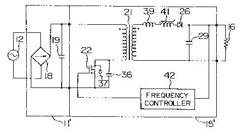
Referring to Fig. 2, a switching regulator
15 according to a preferred embodiment of this invention
may be an on-on type resonant regulator, namely, a
forward converter like in Fig. 1 and therefore comprises
similar parts designated by like reference numerals.
Like in Fig. 1, the illustrated switching regulator
20 comprises an input rectifying circuit 11' and a
converter section 15'. In the example, the input
rectifying circuit 11' is similar in structure to that
illustrated in Fig. 1 except that the input line filter
17 is removed from Fig. 2 but is operable in a manner
25 similar to that illustrated in Fig. 1. In any event,
the input a.c. voltage is produced from the input power
source 12 and is supplied through the input rectifier
circuit 18 and the input capacitor 19 to be impressed as
20245~8
the rectified voltage across the input terminals of the
converter section 15'. In Fig. 2, the primary
transformer 21 is included in the converter section 15'
and has a primary winding and a secondary winding which
5 form parts of primary and secondary circuits,
respectively.
In Fig. 2, the primary circuit comprises a
switching transistor, namely, a main transistor 22
connected in series to the primary winding of the main
10 transformer 21 to form a primary series circuit. A
capacitor 36 is connected in parallel to the switching
transistor 22. The illustrated switching transistor 22
is operable as a diode specified by an internal diode 37
when it is turned off, as shown in Fig. 2.
On the other hand, the secondary circuit
comprises an inductance element 39 which may be formed
either by a leakage inductance of the main transformer
21 or by an external inductance. Like in Fig. 1, the
illustrated secondary circuit comprises a diode 26
20 identical with the first diode 26 of Fig. 1 and an
output capacitor 29 connected across the output
terminals.
It is to be noted that a saturable reactor 41 is
also included in the secondary circuit and has no
25 control winding, as readily understood from Fig. 2. The
saturable reactor 41 exhibits a high impedance during an
off-state of the diode 26 and a low impedance during an
on-state of the diode 26. The high impedance falls
11 20245~8
within a range between 100 kilohms and 500 kilohms while
the low impedance is smaller than 1 ohm and may be, for
example, 0.01 ohm.
The inductance element 39, the saturable reactor
5 41, the diode 26, and the output capacitor 29 are
connected in series to one another in the secondary
circuit of the main transformer 21, as illustrated in
Fig. 2. Like in Fig. 1, the output capacitor 29 is
connected in parallel to the load resistor 16.
Moreover, a frequency controller 42 is connected
between one of the output terminals and the switching
transistor 22. The frequency controller 42 is operable
in response to the output voltage and produces a
sequence of switching control pulses which are specified
15 by an on-state time interval variable in accordance with
the output voltage and an invariable off-state time
interval. As a result, the control pulses have variable
frequencies. Thu~, the switching transistor 22 is
repeatedLy turned on and off in response to the
20 switching control pulses of the variable frequency.
As readily understood from Fig. 2, the diode 26
is put into a conductive state or an on-state when a
positive voltage is impressed across the primary winding
of the main transformer 21 and when the switching
25 transistor 22 is turned on. On the other hand, the
diode 26 is put into an off-state while the switching
transistor 22 is turned off as will later become clear
as the description proceeds. In this connection, the
12 20245~8
illustrated switching regulator is called the forward
converter, as mentioned before.
As described above, the diode 26 is repeatedly
put into the on-state and the off-state in cooperation
5 with the switching transistor 22. A diode switching
period is formed by a time interval of the on-state and
a time interval of the off-state. The time intervals of
the on-state and the off-state will be named an on-state
time interval and an off-state time interval.
Referring to Fig. 3, the secondary circuit of
the switching regulator illustrated in Fig. 2 is
equivalently represented by a circuit shown in Fig. 3
during the on-state time interval of the diode 26.
During the on-state time interval, the diode 26 becomes
15 conductive and a forward voltage drop of the diode 26
may be therefore néglected because the forward voltage
drop is sufficiently small. In addition, the output
capacitor 29 is replaced in Fig. 3 by a constant voltage
source 45 on the assumption that the output capacitor 29
20 has a sufficiently large capacitance. Furthermore,
another constant voltage source 46 specifies an induced
voltage which appears across the secondary winding
during the on-state time interval of the main
transformer 21 and may be referred to as an additional
25 constant voltage source. The induced voltage is
invariable and is therefore a constant voltage.
Herein, it is surmised that the rectified
voltage across the input capacitor 19 (Fig. 2) and the
13 202~5a8
constant voltage of the constant voltage source 46 are
represented by El and E2, respectively, and that the
primary and the secondary windings have first and second
turns Nl and N2, respectively. Under the circumstances,
5 the constant voltage E2 is given by:
E2 = (N2/Nl)-El.
When an inductance of the inductance element 39
and the output voltage, namely, the constant voltage of
the constant voltage source 45 are represented by L and
10 V0, respectively, a current IL which ~lows through the
inductance element 39 is given by:
IL = (E2 - V0)~t/L = ((N2-El/Nl) - V0))-t/L.
On the other hand, an inverse voltage takes
place across the secondary winding of the main
15 transformer 21 during the off-state time interval of the
diode 26. In this event, no current is caused to flow
throuqh the inductance element 39 even when such an
inverse voltage takes place. This is because such a
current is interrupted by the diode 26.
Referring to Fig. 4, description will be made
about operation of the switching regulator illustrated
in Fig. 2. In Fig. 4, a capacitor voltage (depicted at
Vc) across the capacitor 36 is shown along a top line of
Fig. 4 while a current (depicted at ITl) flowing through
25 the primary winding of the main transformer 21 is
illustrated along a second line of Fig. 4. In addition,
a current (depicted at IL) flowing through the
14 2024588
inductance element 39 is shown along a bottom line of
Fig. 4 and may be called a coil current.
When the on-state time interval and the
off-state time interval of the diode 26 are represented
5 by Ton and Toff, respectively, an average value of the
coil current IL, namely, the output current (depicted at
Io) is given by:
~Ton
Io = l/(Ton + Toff ,J IL dt
= (((N2-El/Nl) - Vo)/(2L))-(l/((l/Ton) + (Toff/Ton ))).
(1)
Under the circumstances, when a resistance of
the load resistor 16 is represented by R, the output
15 voltage Vo is given by:
Vo = R-Io. (2)
Substitution of Equation (1) into Equation (2)
gives:
Vo = N2-El/(Nl-(l + (2L/R).((l/Ton) + (Toff/Ton2)))).
(3)
From Equation (3), it is understood that the
output voltage Vo can be stabilized by controlling the
on-state time interval Ton in response to a variation of
the d.c. input voltage-El and the load resistor 16.
Herein, let switching operation of the switching
transistor 22 be carried out within a comparatively low
frequency which is lower than 100 kHz. In this case,
the leakage inductance of the main transformer 21 and
the like may be neglected and L may be therefore
20245~8
considered to be equal to zero. Therefore, Equation (3)
is modified into:
Vo = N2-El/Nl. (4)
It is apparent from Equation (4) that the output
5 voltage Vo can not be stabilized within a low frequency
band because the turns Nl and N2 are invariable and the
output voltage Vo is determined only by the input
voltage El. This shows that the smoothing circuit and
the commutation diode, such as 27, are necessary for
10 stabilizing the output voltage Vo in the low frequency
band.
However, when the leakage inductance of the main
transformer 21 can not be neglected or when the external
inductance element is connected in addition to the
15 leakage inductance, an inductance L of such inductance
elements can not be neglected from Equation (3).
Accordingly, it is possible to stabilize the output
voltage Vo without any smoothing circuit by controlling
the on-state time interval Ton, as is apparent from
20 Equation (3).
Referring to Fig. 5, description will be made as
regards an equivalent circuit of the switching regulator
which specifies a state appearing during the off-state
time interval of the diode 26. In this event, the
25 switching transistor 22 is also put into the off-state,
namely, a cut-off state. Therefore, the secondary
circuit of the transformer 21 may be neglected from the
equivalent circuit.
20245~8
16
Herein, an input voltage (depicted at Vin)
across the input capacitor 19 is represented by a d.c.
voltage source 51. Let an excitation current Imo be
caused to flow through the primary circuit of the main
5 transformer 21 when the switching regulator is seen from
a primary side of the main transformer 21. In addition,
let a primary inductance of the main transformer 21 be
represented by Ll. Under the circumstances, the
excitation current Imo is given by:
Imo = El-Ton/Ll.
The excitation current Imo may be considered as
an initial current which flows through the primary
inductance or coil Ll. Herein, an initial voltage
across the capaci*or 36 of a capacitance C is assumed to
15 be equal to zero without loss of generality. In this
case, a free oscillation is caused to occur due to the
primary inductance Ll and the capacitance C in the
illustrated circuit, as illustrated in Fig. 4. Under
the circumstances, a voltage Vc across the capacitor 36
20 and the current Im flowing through the primary
inductance Ll are given by:
Vc = ~ Imo sin(t - Ton)/ ~ , and
Im = Imo cos(t - Ton)/ ~ .
In Fig. 4, a voltage appears across the
25 secondary winding of the main transformer 21 and is
determined by the output voltage Vo at a time instant at
which the voltage Vc across the capacitor 36 is returned
17 2~245~8
back to zero. Consequently, the diode 26 is put into
the on-state.
Immediately after the diode 26 is turned on, as
mentioned before, namely, for a clamp duration between 0
5 to Tcp, the excitation current of the main transformer
21 serves to feed electric power back to the input
capacitor 19 and to supply electric power to the output
capacitor 29. For the clamp duration, a primary current
ITl is caused to flow through the internal diode 37 of
10 the switching transistor 22 in a reverse direction.
Such a primary current ITl is linearly attenuated as
illustrated in Fig. 4.
If the switching transistor 22 is turned off for
the clamp duration, the capacitor 36 starts to charge at
15 a time instant at which the primary current ITl of the
reverse direction becomes zero. Consequently, a voltage
takes place across the switching transistor 22. Taking
this into consideration, it is possible to avoid
occurrence of such a voltage during the on-state of the
20 diode 26, if the switching transistor 22 is kept in the
on-state within the clamp duration between 0 and Tcp.
When the switching transistor 22 is turned off,
a current which flows through the switching transistor
22 is immediately stopped while the excitation current
25 of the main transformer 21 is caused to flow through the
capacitor 36. Therefore, the voltage across the
switching transistor 22, namely, the voltage across the
capacitor 36 sinusoidally increases after the switching
18 20245~8
transistor 22 is turned off, as illustrated in Fig. 4.
This shows that the voltage across the switching
transistor 22 is developed after the current which flows
through the switching transistor 22 is stopped.
5 Accordingly, no switching loss occurs in the illustrated
switching regulator because the voltage is not crossed
or intersected with the current during the off-state
time interval of the switching transistor 22. In
addition, when the main transformer 21 is put into the
10 clamp state, the switching transistor 22 is turned on at
a time instant within the clamp duration. In this case,
no switching loss occurs due to intersection of the
voltage and the current because the voltage is equal to
zero within the clamp state.
Furthermore, when the voltage has a sinusoidal
wave, no switching noise appears due to parasitic
capacitance and parasitic inductance which might bring
about ringing. Therefore, it is possible to remove the
input line filter 17 and the snubbers 23, 27, and 28 all
20 of which are illustrated in Fig. 1.
In Fig. 2, the capacitor 36 and the inductance
element 39 may be replaced by a depletion layer
capacitance of the switching transistor 22 and a leakage
inductance of the main transformer 21, respectively.
In the illustrated example, the saturable
reactor 41 is added to the secondary circuit of the main
transformer 21 and has the high impedance and the low
impedance when the saturable reactor 41 is put into an
;
19 202458.8
off-state and an on-state, respectively, as mentioned
before. The saturable reactor 41 serves to suppress a
steep residual current which otherwise flows due to the
leakage inductance appearing when the diode 26 is turned
5 off. This enables a reduction of attenuation in a
voltage oscillation wave when the switching transistor
22 is turned off. Thus, the illustrated switching
regulator can favorably realize zero voltage switching
(ZVS) .
As mentioned before, the on-state time interval
of the switching transistor is controlled by using
inductance of the leakage inductance or the external
inductance. With this structure, it is possible to
stabilize the output voltage without the smoothing
15 circuit and the commutation diode. Inasmuch as the
inductance of the main transformer is resonant with the
capacitance connected in parallel to the switching
transistor, the switching transistor is supplied with
the voltage of the sinusoidal wave. Consequently, low
20 loss and high efficiency can be accomplished by the
illustrated switching regulator. In addition, it is
possible to dispense with a noise filter for a reduction
of noise and snubbers.
Inasmuch as the saturable reactor is connected
25 to the secondary circuit of the main transformer, it is
possible to suppress a steep current resulting from the
leakage inductance when the diode 26 is turned off.
Since the saturable reactor exhibits a high impedance
= =
~ ' . . 20245~8
characteristic when the saturable reactor is put into an
off state, attenuation of the voltage oscillation wave
can be reduced when the switching transistor is turned
off. This makes it possible to improve an average
5 efficiency due to the ZVS. Accordingly, the switching
regulator is simple in structure and compact in size and
has a high reliability.