Note: Descriptions are shown in the official language in which they were submitted.
:
2!D~ ~7~
OPTICAL INTERCONNECTION APPARATUS
FIELD OF THE INVENTION
This invention relates to an optical
interconnection apparatus, and more particularly to, an
optical interconnection apparatus using a matrix of
optical funtionable devices.
., .
, BACKGROUND OF THE INVENTION
In these days, optical input and output
x~ apparatus, optical transmission apparatus, optical
switching apparatus, optical signal processing
apparatus, etc. having a large amount of signal
capacity and a property of high speed are required to
.~ be put into a practical use, as information society has
been highly advanced. In this point, a computer
consisting of electronic circuits has a limitation.
Therefore, an optical computer using the high speed of
light and the parallel property thereof is expected to
be developed. On the other hand, a neural network
using optical interconnection is intensively studied to
provide a practical structure. In this neural network,
unit elements each defined as "neuron" are connected by
. .
interconnections, so that an output signal is obtained
from input signals by changing coupling degrees among
neurons. That is, all of input signals are added to
provide a sum whirh is compared with a threshold value
. .
:,. . , ~;;
. :. - .~; :
- 2~2~77~
to provide an output signal.
At the present stage, one type of a neural
network is structured by integrated electronic devices.
In this neural network, an interconnecting portion of
the electronic devices may be replaced by optical
devices. Another type of a neural network is
' structured totally by optical functional devices. In
, any structure, an extremely large number of
interconnections must be done to provide a large scaled
neural network. In this point,light provides effective
means for interconnections among neurons of a neural
network, because the spatial transmission of
information can be carried out by use of light, and a
high density of interconnections can be reali~ed due to
no mutual interference of light signals.
In an optical neural network, spatial light
modulating devices must be provided to change a
coupling degree for each interconnection. For this
purpose, liquid crystal displays are only used in the
optical neural network. However, the liquid crystal
displays have a disadvantage in that an operating speed
is ordinarily as slow ~s several m sec., so that a high
speed operation can not be realized. Otherwise, such
devices as using non-linear materials or semiconductors
. ~ .
are utilized as optical processing devices having high
operating speeds in the optical neural network.
However, these devices have a disadvantage in that the
.,
, .
; ,. ~ ,
.:
.. .. .
3 2~2~7~
high density formation of device arrangement is
difficult to be realized, and because a technology for
arranging the devices in a predetermined pattern is not
sufficiently developed, and electric power consumption
is large.
i In this situation, attention has been paid to an
~ optical functional device with low electric power
'! consumption which is based on an optical thyrister.
,; This device has been described in a report entitled "A
, 10 new double heterostructure optoelectronic switching
device using molecular beam epitaxy" on pages 596 to
600 of "Journal of Applied Physics, Vol. 59, No. 2,
1986", and in a report entitled "Double heterostructure
optoelectronic switch as a dynamic memory with low-
15power consumption" on pages 679 to 681 of "Applied
Physics Letter, Vol. 52, No. 9, 29 February, 1988".
Arbitrary connections using optical
interconnections having a large number of parallel
connections which have been carried out by input
signals are realized by using functions of light
emission, light response, and information storage of
the above described optical functional device.
. .,
i Here, an optical interconnection apparatus using
a matrix of optical functional devices will be
explained, as described in a paper "3a-ZA-2" on page
795 of "Extended abstracts, The 36th Spring Meeting,
1989, The Japan Society of Applied Physics and Related
, , ::
.,~ .
2 ~ 2 ~ r~l 7 ~
Societies, No. 3" held on April 1 to 4 of 1989. This
optical interconnection apparatus comprises a matrix of
optical functional devices and a light receiving
structure. The matrix includes NXN optical functional
5 devices arranged in a matrix pattern, and the light
receiving structure includes N light receiving devices
arranged in a one-dimensional pattern to face the NXN
optical functional devices. In this optical
interconnection apparatus, arbitrary optical
'Yi 10 interconnection are realized by driving predetermined
? optical functional devices which are selected from the
NXN optical functional devices by applying
predetermined signals to signal lines selected from N
X-axis lines and N Y-axis lines. In this operation,
15 each optical functional device has ON state and OFF
state corresponding to binary code states of "0" and
"1", so that the optical functional devices operate as
spatial light modulators. Thus, spatial light
modulated signals are supplied to the light receiving
20 devices. This optical interconnection apparatus has an
advantage in that it operates with a speed much higher
than that of an optical interconnection apparatus using
:
liquid crystal displays.
However, this optical interconnection apparatus
25 has a disadvantage in that coupling degrees are only
set in the connection of information by the binary
values of "0" and "1". Considering that this optical
.,.
,~:
7 ~L
interconnection apparatus is applied to an optical
neural network, an optical arithmetic and calculating
apparatus, etc., it is desired that coupling degrees
change continuously between "0" and "1".
SUMMARY OF THE INVENTION
Accordingly, it is an object of this invention
to provide an optical interconnection apparatus which
operates with a high speed.
It is another object of this invention to
provide an optical interconnection apparatus, in which
arbitrary optical interconnections can be realized.
It is a further object of this invention to
' provide an optical interconnection apparatus, in which
coupling degrees of light information can be changed
continuously between "0" and "1".
According to this invention, an optical
interconnection apparatus, comprises:
a matrix of optical functional devices each
having at least first and second driving terminals, the
first driving terminals being connected to a common
electrode in each row of the matrix, and the second
driving terminals being connected to a common electrode
in each column; and
a light receiving structure of light receiving
devices arranged in a one-dimensional pattern, the
light receiving devices receiving light signals emitted
,, :,
' ~. . , `' " ` '
.
- 2~2~77~
6 71885-16
from the optical functional devices; wherein the matrix of the
optical functional devices are divided into plural device units
'J' each including at least two optical functional devices in the
'. matrix and being optically coupled to a corresponding one of the
. light receiving devices and the at least two optical functional
devices have light transmitting coatings each having a
transmission factor different from others.
According to another aspect of the inventlon, there is
provided an optical interconnection apparatus, comprising: a
matrix of optical devices, each of which includes an anode and a
cathode, each of said anodes being connected to a common electrode
in each row of said matrix, and each of said cathodes being
connected to a common electrode in each column of said matrix; and
light receiving devices arranged in a one-dimensional pattern,
said light receiving devices receiving signal emitted from said
optical devices; wherein said matrix of said optical devices is
divided into multiple units, each of which includes at least two
optical devices, said units being optically coupled to
corresponding light receiving devices, said optical devices being
:~i 20 controlled such that any combination of optical devices within a
unit simultaneously illuminate a single light receiving device.
According to yet another aspect of the invention, there
;. is provided an optical interconnection apparatus, comprising: a
.~ matrix of optical devices, each of which is connected to a common
i row electrode and a common column electrode, said matrix of said
-, .
P~ optical devices being divided into units, each of said units
: including at least two optical devices, and a plurality of
receiving devices arranged in a one-dimensional pattern, each
.,,
~D,
':: ~,t'Oj
.'.' ~.
?~
., , ~ . . . .
.~ . . ~ . -: -
- :
, . .
... .. .
6a 2 ~ ~ ~7 7 ~ 71885-16
receiving device being optically coupled to a corresponding unit,
wherein each unit is controllable to transmit more than two levels
of light intensity to a corresponding one of said receiving
devices.
o In this invention, optical functionable devices with low
electric power consumption which are based on optical thyristors
are arranged in a two-dimensional pattern to provide a light
emitting matrix. Driving terminals of the same kind for each
device are connected to a signal line in each column and each row
by use of common electrodes, so that interconnections of a matrix
pattern are obtained. Each device has functions of light
emission, threshold, and information storage, and is set into ON
state by the application of a voltage larger than a threshold
value across two terminals thereof. This ON state is held by the
application of a holding voltage smaller than the turning-on
voltage across the two terminals. The device which is under ON
state emits light by the application of a predetermined additional
voltage across the two terminals. This light emission is not
obtained in devices which are not under ON state.
,~,
.; .
-
~ ~ 2 ~
. .
` 7
:::
Accordingly, if the devices which are arranged in a
matrix pattern are sequentially addressed to be
selectively turned on, light emission is obtained from
the selected devices by applying a predetermined signal
~ 5 voltage thereto. The emitted lights are supplied to
* light receiving devices which are arranged in a one-
dimensional pattern, so that signals can be transmitted
to designated destinations.
In particular, optical functional devices which
10 are arranged in a matrix pattern are divided by plural
sets of optical functional devices. Here, each set is
defined to be a device unit, in which each device is
provided with a coating having a predetermined
~, transmission factor different from others. As a
.J, 15 result, when devices are selected to emit light in the
device unit, a coupling degree can be changed in the
mode of changing light signal intensity. For instance,
;~ it is assumed that first, second, third, and fourth
devices of the device unit are provided with no
20 coating, and first to third coatings of supplying
output lights of 1/2 intensity, 1/4 intensity and 1/8
intensity relative to the intensity of the output light
in case of no coating, respectively. The first to
fourth devices are addressed to be selectively turned
25 on in accordance with a coupling degree, and a
predetermined signal voltage is commonly applied to the
. .
} selected devices among the first to fourth devices.
~..
,;~
~,;
: . .
: . -, ,
. : -
2 ~ 2 ~
Consequently, coupling degrees of sixteen (24) steps
` are obtained by changing the selection of the four
devices at the time of addressing. When the device
unit includes n optical functional devices in number,
coupling degrees of 2n steps can be obtained.
, BRIEF DESCRIPTION OF THE DRAWINGS
This invention will be explained in conjunction
with appended drawings, wherein:
Fig. 1 is a schematic perspective view showing a
conventional optical interconnection apparatus;
' Fig. 2 is a block diagram showing an optical
interconnection apparatus in a preferred embodiment
according to the invention;
Fig. 3 is a schematic perspective view showing a
matrix of optical functional devices and a light
receiving structure in the preferred embodiment;
Fig. 4 is a plan view showing coatings provided
on the matrix of the optical functional devices in the
preferred embodiment;
Fig. 5 is a schematic cross-sectional view
showing an optical functional device used in the
preferred embodiment; and
Fig. 6 is a timing chart showing operation in
the preferred embodiment.
DESCRIPTION OF THE PREFERRED EMBODIMENTS
~ 2 ~ 2 !~ 6~ 7 ~
.. g
',
Before explaining an optical interconnection
apparatus in the preferred embodiment according to the
x invention, the conventional optical interconnection
apparatus will be explained in Fig. 1.
j S This conventional optical interconnection
, apparatus comprises a matrix 41 of NXN optical
functional devices 4111, 4112, 4113, 4114, -
light receiving structure 42 of light receiving devices
421~ 422, 423 and 424 arranged in a one-dimensional
pattern to face the matrix 41, where the number N is
i four. In the matrix 41, the optical functional devices
4111~ 4112~ 4113~ 4114, ---- are connected to signal
lines X1, X2, X3 and X4 for input signals by each
column, and to signal lines Y1, Y2, Y3 and Y4 for
address synchronous signals by each row. Otherwise,
the light receiving devices 421~ 422, 423 and 424 are
~'4~t connected to signal lines Z1, Z2~ Z3 and Z4 for output
signals in the light receiving structure 42,
respectively.
In operation, address synchronous signals are
sequentially applied to each row of the optical
functional devices 4111, 4112, 4113, q114, .. by the
` signal lines Y1, Y2, Y3 and Y4, while destination
address signals are selectively applied to each column
thereof in synchronism with the address synchronous
signal by the signal lines X1, X2, X3 and X4 If it is
~ assumed that the four optical functiona] devices 4112,
.''.
;. :
,~ .
s' , .. -' :,
. ~ - : , :~ ,, ................ :
.. . .
:,:. ;, . . .
2 ~
.,
"
."! 4124, 4131 and 4143 are selectively turned on, light
emission is obtained from the selected devices, when
information signals are applied thereto at
, predetermined timings. Light signals thus obtained are
;i 5 received by the light receiving devices 421l 422, 423
and 424 of the light receiving structure 42, as
illustrated by dotted arrows in Fig. 1. Then, output
~, signals are supplied through the signal lines Z1~ Z2
Z3 and Z4 to a following signal processing stage.
Aowever, this conventional optical
interconnection apparatus has the disadvantage as
explained before, although it is not repeatedly
described here.
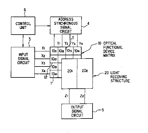
An optical interconnection apparatus in the
preferred embodiment will be explained in Figs. 2 to 4.
This optical interconnection apparatus comprises
a matrix 10 of 4X4 optical functional devices 1011,
1012, 1013, 1014 .... which are arranged in a two-
dimensional pattern, and a light receiving structure 20
of light receiving devices 201 and 202 which are
arranged in a one-dimensional pattern to face a light
emitting surface of the matrix 10. The matrix 10 is
connected through matrix signal lines X1, X2, X3 and X4
to an input signal circuit 3, from which destination
address signals for designating destinations of
information signals, and information signals to be
transmitted to the designated destinations are
.,
~,
.-
7 :~
, 11
; sequentially supplied to selected optical functional
' devices of the matrix 10, and is connected through
matrix signal lines Y1, Y2, Y3 and Y4 to an a
:,
!~ synchronous signal circuit 4, from which address
~ 5 synchronous signals are sequentially supplied to the
qs matrix 10 by each row. The light receiving devices 21
. and 202 of the light receiving structure 20 are
connected through output signal lines Z1 and Z2 to an
output signal circuit 5, in which output signals
10 supplied from the light receiving structure 20 are
processed. The input signal circuit 3, the address
synchronous signal circuit 4, etc. are controlled by a
control unit 6.
s The matrix 10 is divided into four device units
s 15 101, 102, 103 and 104 by vertical and horizontal lines
11 and 12, as shown clearly in Fig. 4. Each of the
four device units 101, 102, 103 and 104 includes 2X2
optical functional devices. For instance, the device
unit 101 includes the optical functional device 111
having no coating, and the optical functional devices
112, 121 and 1022 having coatings of transmission
factors for supplying output lights having intensities
of 1/2, 1/4 and 1/8, respectively, relative to that of
an output light obtained from the optical functional
25 device 111. The device units 102, 103 and 104 have
the same structure as the device unit 11. Therefore,
coupling degrees of sixteen steps are obtained for
~,
,'~
: .
.. ;: . . , :
~ . .. ..: - :.. .
:.- ,-,
~ : : ,
; -`
2~2~ ~7:~
12
light signals supplied from the matrix 10 to the light
receiving structure 20. Such a coating is provided on
an optical functional device, for instance, by
evaporating a metal such as Cr, etc. thereon.
Fig. 5 shows one type of an optical functional
device having a thyristor structure which is applied to
the matrix 10. This optical functional device
comprises epitaxial layers which are grown on a semi-
insulating GaAs substrate 33 by molecular beam epitaxy.
10 These epitaxial layers are an n-GaAs buffer layer 34,
an n-Al0 4GaO 6As layer 35, a p-GaAs layer 36, an n-
GaAs active layer 37, a p-Alo 4GaO 6As layer 38, and a
p-GaAs layer 39. This optical functional device
further comprises an anode electrode 31 provided on the
15 p-GaAs contact layer 39, a cathode electrode 32
provided on the n-GaAs buffer layer 34, an n-gate
electrode 41 provided on the n-GaAs layer 37, and a p-
gate electrode 42 provided on a Zn-diffusion region 40
provided through the n-GaAs layer 37 into the p-GaAs
20 layer 36. This optical functional device is a device
having properties of a threshold value and light
emission, and is turned on to shift into an operating
state by the application of a voltage equal to or
higher than the threshold value across the anode and
25 cathode electrodes 31 and 32 thereof. This operating
state is held by applying a voltage equal to or higher
than a holding voltage across the anode and cathode
:.. ;~ . ::. ~ ~ ' :
2~77~
13
electrodes 31 and 32. In this operating state, the
optical functional device emits light by the
application of a predetermined voltage lower than the
threshold voltage and higher than the holding voltage
thereto. Otherwise, an optical functional device which
is not turned on due to no application of the threshold
voltage thereto does not emit light, even if the
predetermined voltage is applied across the anode and
cathode electrodes 31 and 32 thereof. The optical
10 functional device which is under the operating state is
controlled to be back to non-operating state by the
. application of a voltage lower than the holding
voltage. This optical functional device is of a
response speed as high as several hundred MHz. The n
~ 15 and p gate electrodes 41 and 42 function as electron
x and hole extractors to achieve high-speed turn-off.
In operation, the address synchronous signals S
are supplied from the address synchronous signal
, circuit 4 to the matrix signal lines Y1, Y2, Y3 and Y4,
20 and the destination address signals A and information
signals I are supplied from the input signal circuit 3
to the matrix signal lines X1, X2, X3 and X4, as shown
in Fig. 6. The address synchronous signals S are of a
pulse voltage -Vs, and are applied through the matrix
signal lines Y1, Y2, Y3 and Y4 to the matrix 10 in
time-division as shown by t1~ t2, t3 and t4. On the
other hand, the destination address signals A are of a
'!,' ,,
': ' ' , ', .':
,.
' '' ' ' ' '
14
pulse voltage Va larger than a holding voltage Vh, and
are applied to selected signal lines among the matrix
signal lines X1, X2, X3 and X4 corresponding to
selected optical functional devices in each row of the
matrix 10 at each time division t1~ t2, t3 or t4.
At the divisional time t1~ for instance, a
voltage (Va + Vs) obtained by adding the voltage Vs of
the address synchronous signal S and the voltage Va of
the destination address signal A is applied to the
optical functional devices 111 and 1041. This voltage
(Va + Vs) is set to be larger than a threshold voltage
Vth which is ordinarily 2 to 5 V, so that the optical
functional devices 1011 and 1041 is turned on to shift
into the operating state. At the divisional times t2,
t3 and t4, the optical functional devices 1012, 1022
and 1032, 1023 and 1033, and 114 and 1034 are turned
on to shift into the operating state, respectively, as
apparent from the timing chart of Fig. 6. This
operating state is held in the optical functional
.,
r 20 devices thus turned on by the application of a holding
voltage of approximately 1.4 V thereto.
In this circumstance, the information signals I
are applied through the matrix signal lines X1, X2, X3
~ and X4 to the optical functional devices of the matrix
;1 25 10 in a signal line selected mode at timings as shown
in Fig. 6. Thus, light signals are emitted from the
optical functional devices which are under the
.
2~2~7~
operating state. More precisely, the information
signals I are applied to the matrix signal lines X1 and
X2 simultaneously, and to the matrix signal lines X3
- and X4 slmultaneously. As a result, the optical
functional devices 111, 112 and 1022 emit light
signals which are modulated by the respective
transmission factors in the device unit 11 of the
- matrix 10. These light signals thus modulated are
` received by the light receiving device 201 of the light
receiving structure 20, so that the sum of the light
signals are obtained therein to be supplied through the
output signal line Z1 to the output signal processing
circuit 5. At the same time, the optical functional
devices 1014 and 1023 emit modulated light signals in
the device unit 12 of the matrix 10. These modulated
light signals are received by the light receiving
device 202 of the light receiving structure 20, so that
the sum of the light signals are obtained therein to be
supplied through the output signal line Z2 to the
output signal processing circuit 5. In the same
manner, modulated light signals emitted from the device
units 103 and 104 of the matrix are received by the
light receiving devices 21 and 202 of the light
receiving structure 20, respectively.
As described above, two inputs are connected to
two outputs by the changeable coupling degrees, so that
an optical interconnection apparatus having the load-
.
:
16 ~2~
,,,
sum function to provide an output signal generated by
adding inputs is obtained. As a matter of course, when
it is required that the steps of coupling degrees are
increased in number, the number of optical functional
5 devices included in device units of a matrix is
increased.
Although the invention has been described with
respect to specific embodiment for complete and clear
.disclosure, the appended claims are not to be thus
10 limited but are to be construed as embodying all
~modification and alternative constructions that may
Joccur to one skilled in the art which fairly fall
within the basic teachin~ herein set forth.
,, :... . , , . : :