Note: Descriptions are shown in the official language in which they were submitted.
2~25549
-- 1 --
The present invention relates to a method and
apparatus for modulating and driving a semiconductor
laser, or the like, and a system, e.g., a recording
apparatus, using the same.
As a means for generating a light beam a
semiconductor laser is widely used in various systems
since it is inexpensive and compact, and has the
capability of directly performing amplitude modulation
responsive a driving current.
As a drawback, however, the semiconductor laser
has negative temperature characteristics exhibiting
considerable influence on its driving current light
output characteristics.
Furthermore, the temperature of a semiconductor
laser chip increases due to emission losses during
emission, and hence, a decrease in light output occurs.
A laser beam printer is known as a commercially
available system using a light source such as a
semiconductor laser. For example, in the medical field,
a laser printer for recording a medical image obtained by
MR, CT, DSA, or the like onto a photosensitive recording
medium such as a silver chloride film is widely used. A
laser beam which is strength-modulated in proportion to a
picture element density is deflected by a light deflector
to attain main scanning, and a recording medium is moved
in a direction perpendicular to the main scanning
direction to attain sub-scanning, thereby recording a
','~
- 2 - 2025549
multi-gradation halftone image on the recording medium.
Since a laser printer normally performs recording
at a main scanning speed of 1 to 2 msec and a rate of
several seconds per page, an external temperature is left
unchanged during at least one main scanning period, and a
change in light output due to a change in temperature
during this period is caused by a temperature rise due to
an emission loss of the semiconductor laser itself.
As a means for compensating for a light output
variation caused by the change in temperature, a circuit
for continuously monitoring whether or not an emission
level of the semiconductor laser coincides with a
predetermined level (which is constant for a unit
radiation time), and feeding the monitored level to a
driving current, i.e., a so-called APC (Auto Power
Control) circuit is generally used. This circuit is
disclosed in detail in, e.g., USP Nos. 4,237,427,
4,412,331, 4,583,128, 4,625,315, and the like.
In the prior art, however, since the
semiconductor laser is driven and oscillated using an
input current having a rectangular waveform, it is very
difficult to design an APC circuit. In order to increase
extinction ratio (dynamic range) of a light output,
assuming that a system for performing modulation by
changing a pulse width/numbers of one picture element
with a constant light output (pulse width/numbers
modulation), or a system as a combination of the pulse
.
,
202~9
width/numbers modulation and a change in light output
(amplitude modulation) is adopted, a recording speed
(picture element clock frequency) per picture element of
a laser beam printer is as fast as several MHz. For
example, if pulse-width modulation having 8-bit (256)
gradation is performed, minimum pulse width becomes very
small, i.e., several nsec. When control of the
semiconductor laser for generating such a very small
pulse width is to be performed by the APC circuit with
high precision, control speed must be much increased to
several tens of GHz. It is very difficult to
.!_
2025549
1 perform such high-speed control, and a very expensive
circuit is required to realize the high-speed control.
When a normal APC circuit having a stable control
speed is used, the driving speed of the semiconductor
laser driving circuit as a whole must be decreased, and
high-speed pulse width/numbers modulation cannot be
performed.
For these reasons, when a semiconductor laser is
modulated to draw a halftone image, it is difficult to
obtain a good multi-gradation image, e.g., a good
halftone image having 256 gradation levels or more, and
if possible, an increase in cost occurs.
SUMMARY OF THE lNV~N'l'lON:
It is an object of the present invention to
provide a modulation method and apparatus for a
semiconductor laser, or the like, with which an
exposure amount free from a change in temperature can
be obtained, and a system using the same.
It is another object of the present invention to
achieve the above object without using an APC circuit.
It is still another object of the present
invention to provide a modulation method and apparatus
for a semiconductor laser, or the like, with which a
large extinction ratio can be obtained, and a system
using the same.
It is still another object of the present
invention to provide a low-cost and high-speed
2025~ ~9
1 modulation method and apparatus for a semiconductor
laser, or the like, and a system using the same.
It is still another object of the present
invention to provide a recording apparatus which can
obtain a high-precision image at low cost.
It is still another object of the present
invention to provide a recording apparatus which can
obtain a stable image regardless of a change in
temperature.
It is still another object of the present
invention to provide a recording apparatus which can
obtain an image having a large extinction ratio.
It is still another object of the present
invention to provide a recording apparatus which can
obtain a halftone image having a large number of
gradation levels.
It is still another object of the present
invention to provide a recording apparatus which can
obtain an image having a high resolution.
BRIEF DESCRIPTION OF THE DRAWINGS:
Fig. 1 is a schematic view showing the overall
arrangement of a laser printer according to an
embodiment of the present invention;
Fig. 2 is a block diagram showing the first
embodiment;
Fig. 3 is a timing chart for explaining an
operation of the circuit shown in Fig. 2;
~ 2025549
1 Fig. 4 is a graph for explaining a look-up table;
Fig. 5 is a block diagram showing the second
embodiment;
Fig. 6 is a timing chart for explaining an
operation of the circuit shown in Fig. 5;
Figs. 7A and 7s are graphs for explaining an
operation principle of the embodiment of the present
invention;
Fig. 8 is a graph for explaining an operation
principle of another embodiment of the present
invention;
Figs. 9 and 10 are block diagrams showing the
third embodiment;
Fig. 11 is a block diagram showing the fourth
embodiment;
Fig. 12 is a block diagram showing the fifth
embodiment;
Fig. 13 is a timing chart for explaining an
operation of the circuit shown in Fig. 12;
Fig. 14 is a graph for explaining the principle of
the fifth embodiment;
Fig. 15 is a block diagram showing the sixth
embodiment;
Figs. 16 and 17 are timing charts for explaining
an operation of the circuit shown in Fig. 15;
Fig. 18 is a block diagram showing a modification
of the sixth embodiment;
2025549
1Fig. l9 is a timing chart for explaining an
operation of the circuit shown in Fig. 18;
Fig. 20 is a graph showing characteristics of a
semiconductor laser;
5Fig. 21 is a graph for explaining a driving
operation of the semiconductor laser;
Fig. 22 is a graph for explaining the principle of
the sixth embodiment;
Fig. 23 is a block diagram showing the seventh
10embodiment;
Fig. 24 is a timing chart for explaining an
operation of the circuit shown in Fig. 23;
Fig. 25 is a block diagram showing a modification
of the seventh embodiment;
15Fig. 26 is a graph for explaining the principle of
the seventh embodiment;
Fig. 27 is a block diagram showing the eighth
embodiment;
Fig. 28 is a timing chart for explaining an
20operation of the circuit shown in Fig. 27;
Fig. 29 is a block diagram showing a modification
of the eighth embodiment;
Fig. 30 is a circuit diagram of a triangular wave
generator shown in Fig. 29;
25Fig. 31 is a timing chart of the circuit shown in
Fig. 30;
Fig. 32 is a graph for explaining the principle of
2~2~49
an operation the circuit shown in Fig. 29;
Fig. 33 is a block diagram showing another
modification of the eighth embodiment;
Fig. 34 is a timing chart for explaining an
operation of the circuit shown in Fig. 33;
Fig. 35 is an explanatory view showing a case
wherein a jitter occurs in an image;
Fig. 36 is a graph showing driving current-light
output characteristics of a semiconductor laser; and
Fig. 37 is a block diagram for explaining a
conventional APC circuit.
DESCRIPTION OF THE PREFERRED EMBODIMENTS:
1. Principle of Light Modulation Method of the Present
Invention
Fig. 36 shows the driving current light output
characteristics of a semiconductor laser (quoted from
HL8312G Data Book, HITACHI). In Fig. 36, a driving
current [mA] of the semiconductor laser is plotted along
the abscissa, and a light output [mW] is plotted along
the ordinate. Measurements were performed at case
temperatures of 0C, 25C, and 50C. As can be read from
the graph, negative temperature characteristics of
about -0.1 mW/C are observed. This implies that the
light output of the device varies considerably with
variations in external temperature.
Fig. 37 is a block diagram of a known APC circuit
used to compensate for the characteristics of the laser.
202~549
In Fig. 37, a setup current 901 intended to be proportional
to emission level is input to the APC circuit. The APC
circuit includes a voltage adder 902, a voltage-to-current
(V/I) converter 904 for converting a semiconductor laser
driving voltage Vd 903 to an actual driving current Id905,
a semiconductor laser 906, a PIN photodiode 907 for
monitoring a laser emission amount, and a current-to-
voltage (I/V) converter 909 for converting a monitor
current Im 908 into a monitor voltage Vm 910. In order to
monitor light output of the semiconductor laser 906 by the
PIN photodiode 907, the PIN photodiode 907 monitors back
emission of the semiconductor laser at a trailing edge
portion of the laser chip, or monitors light split by a
beam splitter (not shown) arranged in front of the laser
chip. Fig. 37 shows a typical single-loop feedback control
system. Since a difference between the setup voltage Vs 901
and the monitor voltage Vm corresponds to the driving
voltage Vd 903, the light output is always controlled to be
proportional to the setup voltage Vs and not to vary due to
a change in temperature.
The principle of a modulation method
-~'
2025549
-- 10 --
1 according to the present invention will be described
below.
As can be understood from current-light output
characteristics of a semiconductor laser shown in
i Fig. ~, slope efficiency n tmW/mA] almost remains the
same even if a temperature varies. More specifically,
the graph is translated upon a variation in
temperature. In some semiconductor lasers, the slope
efficiency slightly varies. However, these
semiconductor lasers can be used as long as their slope
efficiency values are almost constant in a temperature
environment wherein they are used.
Assume that a mi n imum light output of laser
oscillation of a semiconductor laser is represented by
P0 in Fig. 7A. lt is also assumed that a light
output in an LED oscillation region below P0 can be
ignored. If not ignored, light in an LED region with
poor coherence can be eliminated by an interference
filter or a polarization filter. Assume that a driving
current for outputting the minimum laser oscillation
light output P0 at a given temperature Tl is
represented by io. The driving current of the
semiconductor laser is linearly increased from ior and
an effective value of the light output at that time is
monitored by a detector. If a time is expressed as t
[sec], a current i is assumed to be increased in
proportion to a lapse of time as follows:
2025549
1 i io + kt ................................. (1)
(k is a constant)
When the light output is increased from P0 by P
the driving current is cut off. In this case, the
driving current need not always be completely cut off
to zero, but can be decreased below at least io to be
substantially cut off. In Fig. 7A, the driving
current which is linearly increased is denoted by 91,
and the light output at the temperature Tl is denoted
by 92. An area (time integral value) of the
sawtooth-wave light output 92 corresponds to an
exposure amount E, and is given by:
E = Ps (Po + PS/2~ ...(2)
nk
lS A case will be e~mined below wherein the
temperature of the semiconductor laser chip is
increased from TI ~low temperature) up to T2 (high
temperature). As described above, in temperature
characteristics of the semiconductor laser light
output, it can be considered that the slope efficiency
is not varied, and the current-light output
characteristic curve is translated. In this case, the
minimum laser oscillation light output P0 is left
unchanged, and the driving current io for outputting P0
is changed. The changed current can be approximated as
a current at which the light output in the
current-light output characteristics at the temperature
- 12 ~ 20~55~9
1 T2 is P0. Assume that a driving current for outputting
P0 obtained when the temperature of the semiconductor
laser chip reaches T2 (~ T1) is represented by io' (>
io). Similarly, a change in light output obtained when
a current is linearly increased like in equation (1) is
represented by 93 (broken line) in Fig. 7A. A laser
oscillation begins from ior, and a driving current is
cut off when the light output is increased by Ps~ As
shown in Fig. 7A, since the slope efficiency is left
unchanged, the waveform of the sawtooth-wave light
output 93 r~m~ins the same as that at the temperature
T1, and hence, the exposure amount E is the same as
that expressed by equation (2).
A case will be examined below wherein the present
invention is applied to a laser printer, and the
exposure amount given by equation (2) is that for one
picture element. Even when the temperature of the
semiconductor laser is changed, the exposure amount is
left unchanged, and an exposure position and time are
slightly shifted due to a variation in temperature.
More specifically, when a temperature is increased, the
exposure time is delayed, and the exposure position is
shifted backward. The opposite results are obtained
when a temperature is decreased. When the position and
time shifts due to the variation in temperature are set
to fall within a range of one picture element, and are
less than a resolution of human eyes, this means that a
- 13 -
2025549
1 change in exposure amount due to a change in
temperature can be substantially corrected.
An extinction ratio obtained when the modulation
method of the present invention is used will be
calculated below.
In equation (2), the setup light output Ps can
theoretically become zero, but cannot actually become
zero due to a factor, e.g., a delay time of a control
system, and a minimum value of the setup light output
becomes PSo ~ - If a m~ximum value of the setup
light output is represented by PSl, the extinction
ratio is given by:
Pso(Po + PsO/2) : Psl(PO + Ps1/2) (3)
For example, assuming that PO = 1 mW and the
m~imllm light output of the semiconductor laser is 15
mW, an extinction ratio becomes 1 : lS if strength
modulation is simply performed. If PsO = 1 mW and P
= 15 mW in relation (3), an extinction ratio obtained
according to the modulation method of the present
invention can be greatly increased to 1 : 85. More
specifically, according to the modulation method of the
present invention, a large extinction ratio can be
obtained, and the m~;mum number of gradation levels of
an exposure amount can be increased.
In this manner, the control system of this
embodiment can be relatively simplified since pulse
width control and exposure amount control can be
2025549
- 14 -
1 performed by the same circuit. Since control can be
attained by single ON and OFF operations, a stable
control system can be easily constituted.
In order to further change the exposure amount E,
Ps can be changed in equation (2) to change E.
Instead, an inclination k is changed while Ps is
constant. Alternatively, both k and Ps may be changed
to change E.
When a multi-beam type semiconductor laser having
two laser oscillation mechanisms on a single chip or in
a single housing is used, one semiconductor laser is
driven by a sawtooth wave, and the other semiconductor
laser is pulse-width modulated with a constant current,
so that temperature variation correction of an exposure
amount attained by pulse-width modulation in a
conventional system can be performed by constant
voltage driving. Fig. 8 shows a light output in this
case. In Fig. 8, a light output A represents a light
output of a semiconductor laser driven in a sawtooth
wave, and a light output B represents a light output of
a semiconductor laser driven by a constant current.
Temperatures of the two semiconductor lasers are almost
equal to each other since they are arranged on a single
chip. The light output B is cut off when the light
output A is increased by Ps~ When the temperature is
increased from T1 to T2, the light output B is
decreased by a temperature rise, as shown in Fig. 8.
2025549
1 However, when the temperature reaches T2, a cutoff
timing is delayed accordingly, as shown in Fig. 8, and
an exposure amount (time integral value) of the light
output B ro~i n~ the same at any temperature.
According to the modulation method of the present
invention, light modulation is performed so that a
light output of a semiconductor laser has a
non-rectangular waveform including a waveform increased
as a lapse of a time. The modulation is performed
until a desired exposure amount is obtained, so that a
desired constant exposure amount free from a
temperature variation can be obtained without using an
APC circuit, and a large extinction ratio can be
obtained.
Note that the present invention is not limited to
a semiconductor laser, but may be applicable to a
modulation light source as long as it can be directly
modulated and has similar characteristics. A light
output from a light source need not always be linearly
increased, as shown in Fig. 7A, but may be increased
stepwise, as shown in Fig. 7B. The same applies to a
system to be described below.
2. System Usinq Liqht Modulation Unit
The above-mentioned modulation method is not
limited to a printer but may be widely applied to
various systems which require light modulation. For
example, the modulation method may be applied to an
2025549
- 16 -
1 image recording apparatus such as a printer or a
copying machine, an information recording apparatus for
recording information on an information recording
medium such as an optical disk or an optical card, a
S display apparatus, a machine tool, medical equipment
such as a laser knife or an optical treatment
apparatus, a measurement/inspection apparatus, an
optical communication apparatus, and the like.
(First Embodiment)
An embodiment wherein the present invention is
applied to a laser printer, widely used in, e.g., the
medical field, for recording a high-definition,
multi-gradation halftone image on a film, will be
described in detail below with reference to the
drawings. In the apparatus of this embodiment, a
halftone image having as many as 4,096 gradation levels
can be drawn.
Fig. 1 shows the arrangement of the entire system
of the laser printer. The system includes a
semiconductor laser controller 8 for modulating and
driving a semiconductor laser. A unit 19 includes an
interface for fetching original image data from an
external equipment such as MR, CT, DSA, or the like, an
image memory for storing image data consisting of a
large number of picture element data, and an image
processing circuit for performing image processing such
as image array processing, variable magnification
~025549
- 17 -
1 processing, and the like. The image processing circuit
performs variable magnification processing such as
enlargement or reduction processing of an original
image in accordance with a predetermined output format.
When an image is to be enlarged, the image processing
circuit performs picture element interpolation
processing using a known method such as Nearest
Neighbor Interpolation, Linear Interpolation, Cubic
Spline Interpolation, or the like.
The system also includes a semiconductor laser 1,
an optical system (e.g., a collimator lens) 2 for
collimating light emitted from the semiconductor laser,
an aperture stop 3, a beam splitter 4, a focusing lens
6, and a PIN photodiode 7. An output from the
photodiode 7 is input to the semiconductor laser
controller 8 to monitor a strength of a laser beam
split by the beam splitter 4. A lens 5 and a rotary
polygonal mirror 9 for performing main scanning are
arranged in a straight transmission direction of the
beam splitter 4. The system also includes an f-0 lens
10 for inclination correction, a reflection mirror 11
for reflecting a light beam in a direction
perpendicular to a sheet-like photosensitive recording
medium 12 such as a silver chloride film.
The system further includes a supply magazine 16
for storing sheet-like recording media, a receive
magazine 17 for storing photosensitively recorded
- 18 - 2025549
1 recording media, and a sUb-scAnn i ng motor 13. A roller
14 is connected to the motor 13 to sub-scan the
sheet-like recording medium 12. An encoder 15 is
mounted on the rotational shaft of the roller 14 to
detect a rotational state of the roller 14. As the
encoder 15, for example, a laser rotary encoder is
suitable. The recording medium 12 is picked up from
the supply magazine 16, and is fed to the roller 14.
The recording medium 12 is then subjected to exposure
recording by a light beam while being sub-scanned by
the roller 14 at a low speed. The recorded medium is
stored in the receive magazine 17. Note that the
recorded medium may be directly fed not to the receive
magazine 17 but to an automatic developing machine (not
shown).
A photodiode 18 is arranged to obtain a signal
(BD) signal for representing the beginning of each main
scAnning period so as to take synchronization in units
of main scAnning periods. The semiconductor laser
controller 8 modulates and drives the semiconductor
laser 1 on the basis of a content of an image memory 19
for storing picture element data in synchronism with an
output from the photodiode 18. Since a drawing start
timing of each scanning line is obtained on the basis
of the BD signal, the BD signal must be obtained at an
accurate timing as much as possible so as to draw a
high-quality image. Thus, when a scanning light beam
2 0~55 4 9
-- 19 --
1 passes through the photodiode 18 to detect a signal,
the semiconductor laser 1 is continuously oscillated to
have a constant output. In order to prevent diffused
reflection at, e.g., a corner portion of the rotary
polygonal mirror, the light output of the semiconductor
laser 1 is forcibly stopped in a blanking period other
than a period wherein light is incident on the
photodiode 18.
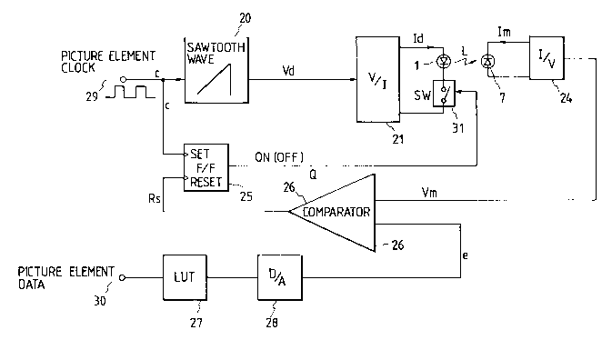
Fig. 2 is a detailed block diagram of a unit
illustrated as the semiconductor laser controller 8 in
Fig. 1, and a description will be made below with
reference to Fig. 2.
In Fig. 2, a setup value 30 for controlling a
light output is 12-bit (4,096 gradation levels) digital
data which is set according to a density of recording
picture elements. The circuit shown in Fig. 2 includes
a look-up table 27, serving as a means for correcting
an exposure amount to be proportional to a square of
the setup value, for converting picture element data, a
digital-to-analog (D/A) converter 28 for converting
corrected picture element data into an analog value, a
comparator 26 for comparing the detected light output
and picture element data, a flip-flop 25 which is
set/reset in response to a leading edge of an input,
i.e., which is set by a picture element clock, and is
reset by an output from the comparator 26, a sawtooth
wave generator 20 for outputting a sawtooth wave
2025549
- 20 -
1 synchronized with a picture element clock, a
voltage-to-current (V/I) converter 21 for converting
the sawtooth wave into a driving current for the
semiconductor laser 1, a switch 31 which is turned
on/off by an output Q from the flip-flop 25, and a
current-to-voltage (I/V) converter 24 for converting a
current detected by the PIN photodiode 7 into a
voltage.
The operation of the above-mentioned arrangement
will be described below with reference to the timing
chart shown in Fig. 3. In Fig. 3, C represents a
picture element clock. e represents an analog value
obtained by converting 4,096-level picture element data
input in synchronism with the picture element clock by
lS the D/A converter 28. Q represents an output from the
flip-flop 25. The output Q ON/OFF-controls the switch
31. Vd represents an output from the sawtooth wave
generator 20, i.e., an input to the V/I converter 21,
and v0 represents an offset corresponding to a mi n i mum
current for causing the semiconductor laser to perform
laser oscillation. Id represents a driving current of
the semiconductor laser. When the output Q is enabled,
a current according to Vd flows, and when the output Q
is disabled, no current flows. L represents a light
output from the semiconductor laser. Rs represents an
output from the comparator 26. When the output e from
the D/A converter 28 is larger than an output from the
20255~9
1 ItV converter 24 as a detection value of the light
output, the output Rs goes to high level; otherwise, it
goes to low level. The output Q from the flip-flop 25
is reset in response to the leading edge of the output
Rs.
In Fig. 3, the output Q from the flip-flop 25 goes
to high level in response to a leading edge 60, and the
switch 31 is turned on. When the switch 31 is turned
on, the semiconductor laser begins to perform laser
oscillation. When the light output L exceeds the
output from the A/D converter, the output Rs goes to
high level, and the flip-flop is reset at its leading
edge 61. Thus, the flip-flop cuts off the light
output, so that the light output forms a sawtooth
waveform. With this operation, as described above, an
exposure amount of the light output does not depend on
a change in temperature, and depends on only the output
_ from the D/A converter.
An exposure amount is given by equation (2) in
which Ps is replaced with e, i.e., is represented by a
quadratic expression associated with e. Therefore, the
look-up table 27 for causing the exposure amount to be
proportional to the picture element data 30 is obtained
based on equation (2). Fig. 4 shows conversion
characteristics of the look-up table. In Fig. 4, a
curve 72 represents a waveform of an exposure amount
(equation (2)), and a curve 71 represents the look-up
2025549
.
- 22 -
1 table.
(Second Embodiment)
Fig. 5 is a block diagram of the second embodiment
according to the present invention. The same reference
numerals in Fig. 5 denote the same or similar parts as
in Fig. 2. The characteristic feature of this
embodiment is that a triangular waveform having the
same rise and fall speeds (inclinations) is used as a
driving current for a laser. Note that the rise and
fall speeds need not always be the same.
The circuit shown in Fig. 5 includes a comparator
26 for comparing a detected light output and picture
element data, a flip-flop 25 which is set/reset in
response to a leading edge of an input, i.e., which is
set by a picture element clock, and is reset by an
output from the comparator 26, an AND gate 35 used to
control a duty of a rectangular wave output Vs. The
circuit also includes an integrator 36 for waveshaping
a rectangular wave into a triangular wave Vt, a
comparator 37 for outputting a voltage vO for flowing a
m;n;mum current for causing a semiconductor laser to
perform laser oscillation, an adder 38 for adding the
triangular wave Vt and vO to output a driving voltage
Vd, a V/I converter 21 for converting the driving
voltage Vd into a driving current for the semiconductor
laser 1, and an I/V converter 24 for converting a
current detected by the PIN photodiode 7 into a
- 2025549
- 23 -
1 voltage.
The operation of the above-mentioned arrangement
will be described below with reference to the timing
chart of Fig. 6. In Fig. 6, C represents a picture
element clock, and e represents an analog value
obtained by converting picture element data input in
synchronism with the picture element clock by the D/A
converter 28.
Vs represents an output from the AND gate 35. The
output Vs is a rectangular wave which is synchronous
with the picture element clock, and whose duty is
controlled by an output from the flip-flop 2S. Vt
represents a triangular wave output from the integrator
36. Vd represents an input voltage to the V/I
converter 21. If Vt > O, the voltage Vd is obtained by
adding vO to Vt, and if Vt = O, it is obtained by
adding O to Vt. By adding the output from the
comparator 37, the semiconductor laser 1 performs laser
oscillation from the beginning of the leading edge of
the triangular wave. L represents a light output from
the semiconductor laser. Rs represents an output from
the comparator 26. When the output e from the D/A
converter 28 exceeds the output from the I/V converter
24 as a detection value of the light output, the output
Rs goes to high level; otherwise, it goes to low level.
The output Q from the flip-flop 25 is reset in response
to a leading edge 63 of Rs.
-
- 24 - ~02~
1 In Fig. 6, the output Q from the flip-flop 25 goes
to high level in response to a leading edge 62, thus
generating the triangular wave Vt. When the triangular
wave is generated, the comparator 37 adds the voltage
vO to the triangular wave to generate Vd. Since a
driving current proportional to Vd flows, the light
output L is generated by the semiconductor laser, as
shown in Fig. 6. When the output L is detected and
exceeds the output e of the D/A converter 28, the
output from the comparator 26 goes to high level, and
the flip-flop 25 is reset in response to the leading
edge of the output from the comparator 26. Thus, the
integrator 36 begins to discharge, and the triangular
wave Vt begins to fall. The fall speed is the same as
the rise speed, and the light output also has a
symmetrical waveform to that upon rising. An exposure
amount defined by this light output has no temperature
dependency like in the first embodiment described
above. The look-up table is the same as that in the
first embodiment.
(Third Embodiment)
Fig. 9 is a block diagram of the third embodiment
according to the present invention. Since Fig. 9 is
substantially the same as Fig. 1 as the block diagram
of the first embodiment, only a difference will be
explained below.
In a sawtooth wave generator 50, an inclination of
- 2025549
- 25 -
1 a sawtooth wave to be generated can be set by an
external electrical input. The inclination is obtained
by converting picture element data into an analog value
by a D/A converter 28. A comparator 26 compares a
light output detected by a photodiode 23 with a
predetermined constant value Ps~ With this
arrangement, when the light output exceeds the constant
value Psl the driving current can be cut off. An
exposure amount E at that time (integral value of the
light output) is given by equation (2) described above.
For the sake of descriptive convenience, equation (2)
is described again.
E = Ps (Po + Ps/2) ...(2)
nk
where n is the slope coefficient of a semiconductor
laser, k is the inclination of the driving current, and
PO is the minimum light output of the semiconductor
laser.
In the first embodiment, k in equation (2) is set
to be constant, and Ps is changed to control the
exposure amount E. In this embodiment, however, Ps is
set to be constant, and k is changed in correspondence
with picture element data, thereby controlling the
exposure amount E.
A means for changing the inclination of the
sawtooth wave by an electrical input can be realized by
a circuit arrangement shown in, e.g., Fig. 10. In
2025549
- 26 -
1 Fig. 10, a picture element clock is input to a
monostable multivibrator to fix a duty ratio, and is
then input to a triangular wave generator using an
operational amplifier. A resistor used in the
triangular wave generator is varied by an electron
volume to change the inclination of the sawtooth wave.
Since this embodiment employs a method of linearly
increasing the light output, and cutting it off at a
given value, a change in exposure amount due to a
change in temperature can be eliminated like in the
first embodiment.
Note that the driving current for the
semiconductor laser is not limited to the sawtooth wave
but may be a triangular wave described in the third
embodiment.
(Fourth Embodiment)
Fig. 11 is a block diagram of the fourth
embodiment. The arrangement of this embodiment is
similar to that shown in Fig. 9. The characteristic
feature of this embodiment is that the input of a
comparator 26 is also connected to picture element
data. In this embodiment, the light amount setup value
Ps is changed in proportion to the inclination k, and a
constant pulse width (for one picture element) is
obtained regardless of a value of picture element data.
This means that the inclination k of the driving
current and the light amount setup value Ps in equation
- 27 ~ 2Q25549
1 (2) are changed at the same time to control the
exposure amount E.
The embodiments so far exemplify a kind of
pulse-width modulation, and a pulse width, i.e., an
exposure time is changed according to a value of
picture element data. When this technique is applied
to an image recording apparatus, a pulse width is
undesirably changed according to a value of picture
element data within one picture element, and an
exposure region within one picture element is deviated.
Furthermore, a degree of deviation is also varied
according to picture element data.
In contrast to this, according to this embodiment,
since the inclination k and the light amount setup
value Ps are simultaneously changed in association with
each other, the pulse width, i.e., the exposure time
can always be kept almost constant. That is, since
almost the entire region within one picture element is
exposed, the deviation and variation of the exposure
region as drawbacks of pulse-width modulation can be
eliminated, thus obtaining high image quality.
In this embodiment, the driving current is not
limited to the sawtooth wave. That is, a triangular
wave may be used to have a waveform symmetrical about
the center of one picture element. When such a
triangular wave is used, the center of density of each
picture element can be aligned at the center in each
- 28 - 2025549
1 picture element, and a density distribution within one
picture element can be uniformed. As a result, a good
halftone image with higher accuracy can be obtained.
In all the above-mentioned embodiments, modulation
is performed once within one picture element. However,
similar modulation may be repeated several times within
one picture element. This operation can be realized by
multiplying an integer constant with a frequency of a
sawtooth or triangular wave in the arrangement of each
embodiment. Thus, a density distribution within one
picture element can be segmented and equalized, thus
obt~ining an image with better image quality.
(Fifth Embodiment)
According to the exposure techniques in the
methods of the embodiments so far, since an exposure
amount is defined by an area of a triangle, it is
always multiplied with a coefficient of 1/2, and a high
exposure amount is difficult to obtain. In order to
increase the exposure amount, a maximum light output
may be increased. However, a light output at a m~i~um
rating of a semiconductor laser is unique to the
semiconductor laser, and the laser cannot be operated
beyond the rating.
In order to solve this problem, according to this
embodiment, when an exposure amount is modulated with a
sawtooth waveform, the light output from the
semiconductor laser is restricted not to exceed a
2025549
- 29 -
1 predetermined value. When the light output reaches the
predetermined value, conventional pulse-width
modulation is performed based on the predetermined
value, thus increasing the exposure amount.
Fig. 14 is a four-quadrant graph for explaining
the operation principle of this embodiment. Quadrant I
shows driving current-light output characteristics of
the semiconductor laser, and exemplifies a case wherein
case temperatures are To and T1 (To < Tl). In this
case, the temperature To is assumed to be an estimated
minimum temperature when an equipment is used. This
assumption is the same as that in the previous
embodiments. A mi n i mum laser oscillation light output
is represented by P0 under an assumption that the light
output must be used below Pm. Quadrant IV shows a
change over time in driving current to be supplied to
the semiconductor laser having the characteristics in
Quadrant I. A driving current is plotted along the
abscissa, and time is plotted along the ordinate. In
Quadrant IV, a driving current i is immediately raised
up to near a minimum oscillation current io at the
temperature To at time t = 0, and thereafter, is
linearly increased relatively slowly. The light output
is monitored, and if the light output reaches Pm~ the
current is set to be a predetermined value, so that the
light output is set to be the predetermined value Pm.
Quadrant II obtains a change over time in light
20255¢9
- 30 -
1 output obtained when the driving current in Quadrant IV
is supplied to the semiconductor laser having the
characteristics in Quadrant I as a combination of
Quadrants I and IV.
Assuming that slope efficiency of a laser
oscillation portion of the semiconductor laser is
represented by n [mW/mA] and an inclination of a linear
rise portion of the driving current i is represented by
K [mA/sec], an exposure amount E1 until the light
output reaches P1 (< Pm) in Quadrant-II is given by an
area of a triangle (O A1 A5) in Fig. 14, and is also
expressed by the following equation in consideration of
the mi n i mum laser light output P0:
E1 = - (p12 _ po2) --(4)
2nK
(Po < Pl < Pm)
When the emission amount setup value is P2 (~ Pm)~
modulation is performed with a pulse width ~x
proportional to (P2 - Pm) after the emission amount
reaches Pm. If a proportional constant at that time is
represented by C, an exposure amount E2 is given by:
E2 = - (pm2 _ po2) + C(P2 ~ Pm) (5)
2nK
(P2 ' Pm)
Since equations (4) and (S) are joined by the setup
value Pm~ C is calculated to equalize differential
coefficients at that time. From equation (4),
- 31 - ~o~ 9
1 dEl Pm .................................... (6)
dPl Pl Pm nK
Therefore, if C = pm/nK~ equations (4) and (5) can be
relatively smoothly joined by the setup value Pm.
Therefore, an exposure amount E is given by the
following equations as a function of the setup value P:
E = (p2 _ po2) (Po - P - Pm)
2nK
E = - (2PPm - ~PO + Pm )) (P ~ Pm)
- 2nK
...(7)
As shown in Fig. 14, when the temperature is
changed from To to T1, an exposure pattern is merely
translated. Therefore, an exposure amount itself is
left unchanged. More specifically, when the setup
value satisfies P1 < Pm~ the exposure amount is defined
by a triangle (O Al A5) at the temperature To~ and is
defined by a triangle (Bo B1 B5) at the temperature T1.
If an LED oscillation region is ignored, the areas of
these two triangles are almost equal to each other.
When the setup value satisfies P2 ~ Pm~ the exposure
amount is defined by an area of a rectangle
(O A2 A3 A4) at the temperature To~ and is defined by
an area of a rectangle (Bo B2 B3 B4) at the temperature
T1. The areas of the two rectangles are almost equal
to each other, and it can be understood that a constant
exposure amount can be obtained regardless of a
2Q ~5~49
- 32 - .
1 variation in characteristics of the semiconductor laser
due to a variation in temperature.
Thus, a varlation in characteristics of the
semiconductor laser due to a variation in temperature,
as a feature of modulation with sawtooth wave, is
automatically compensated, and at the same time, a
function of obtaining a high extinction ratio can be
assured, so that a m~ximum exposure amount can be
increased, and a still higher extinction ratio can be
obtained.
Fig. 12 is a block diagram showing a detailed
arrangement of this embodiment. A circuit block
denoted by 104 constitutes to a sawtooth wave
generator, which is triggered in response to the
leading edge of a picture element clock to generate a
sawtooth wave to a node 153. A sample & hold (S/H)
circuit 120 receives a voltage at the node 153. When a
Hold input of the S/H circuit 120 is at low logic
level, the S/H circuit 120 directly outputs the voltage
at the node 153 to an output 154, and the S/H circuit
120 holds, during a high-level period, the output
voltage obtained when the Hold input goes to high
level. A V/I converter 21 converts the output 154 from
the S/H circuit 120 as an input voltage into a driving
current of the semiconductor laser. An analog switch
31 is enabled while an ON (control) input is at high
level, and is disabled when it goes to low level. A
2~25~4 9
1 reset-set flip-flop 106 is triggered in response to the
leading edge of a SET input, and its Q output goes to
high level. The flip-flop 106 is triggered in response
to the leading edge of a RESET input, and its Q output
goes to low level. The Q output is connected to the ON
control input of the switch. This signal is denoted by
156. A light output current 157 from a photodiode 7 is
converted into a voltage value by an I/V converter
indicated by a block 24, thus outputting a light
voltage 158. A D/A converter 28 converts picture
element data into an analog value, and its analog
output P is denoted by 159. A comparator 108 compares
analog voltages. When a voltage at a "+" input is
higher than that at a "-" input, the comparator 108
outputs high level; otherwise, it outputs low level.
The "+" input is connected to the light output 158, and
the "-" input is connected to the D/A output P 159. A
comparator 109 is similar to the comparator 108. A "+"
input of the comparator 109 is connected to the light
voltage, and its "-" input is connected to a constant
voltage Pm corresponding to the m~ ximum light output.
A reset-set flip-flop 110 is similar to the flip-flop
106. A SET input of the flip-flop 110 is connected to
the output of the comparator 109, and its RESET input
is connected to the picture element clock. An
integrator is indicated by a circuit block 111. The
integrator 111 receives the output from the flip-flop
- 34 ~ 202~5~9
1 110, and generates an integral output of a positive
voltage. The output of the flip-flop 110 is also
connected to the Hold input of the S/H circuit 120. A
differential amplifier serving as a subtracter is
indicated by a circuit block 113. One input of the
subtracter 113 is connected to the constant voltage P
and the other input is connected to the D/A output P
(159). The output voltage of the subtracter 113 is
given by (P - Pm)R2/R1. A voltage comparator 112 is
similar to the comparator 108 or 109. A "+" input of
the comparator 112 is connected to the output 163 of
the integrator 111, and its "-" input is connected to
the output of the subtracter 113. One input of a
2-input AND gate 115 is connected to the output of the
comparator 112, and the other input is connected to the
output of the flip-flop 110. One input of a 2-input OR
gate 107 is connected to the output of the comparator
108, and the other input is connected to the output of
the AND gate 115. The output of the OR gate 107 is
connected to the RESET input of the flip-flop 106.
An operation will be described below with
reference to the timing chart of Fig. 13. In Fig. 13,
(A) represents a waveform of a picture element clock
29, (B) represents the sawtooth wave 153, (C)
represents the light voltage 158, (D) represents the
output 160 from the comparator 108, (E) represents the
~u~r~llt l f;1. frnm th~ f l i n-f l ~n l n~ esents the
_ 35 _ 20255¢9
1 output 162 from the flip-flop 110, and (G) represents
the output 163 from the integrator 111. In Fig. 13,
the sawtooth wave 153 begins to be increased at a
timing of a leading edge 181 of the picture element
clock (A). An offset voltage vO is superimposed on the
sawtooth wave 153 in advance, and is set to be a
voltage corresponding to a current value smaller than a
mi n i mum current value ith for performing laser
oscillation at a mi nimum temperature within a
temperature range normally used by a semiconductor
laser 1 (normally set to near ith). At the same time,
the flip-flop 106 is set, and the switch 31 is enabled.
The semiconductor laser 1 begins to emit light, and the
light voltage 158 obtained by converting light received
lS by the photodiode 7 into a voltage value appears, as
shown in (C) of Fig. 13. The output P (159) of the D/A
converter 28 is illustrated by an alternate long and
short dashed line in (C) of Fig. 13. In addition, the
constant voltage Pm is also illustrated by a broken
line.
Assume that the D/A output P at a timing 181 in
Fig. 13 satisfies P < Pm. In (C) of Fig. 13, when the
light voltage is increased upon an increase in light
output and reaches the value P, the output 160 from the
comparator 108 shown in (D) goes to high level. At
this time, the flip-flop 110 is kept reset, and one
input of the AND gate 115 is kept at low level.
2025549
- 36 -
1 Therefore, the output of the AND gate 115 is kept at
low level, and the output 160 of the comparator 108 is
directly supplied to the RESET input of the flip-flop
106. As a result, the output 161 of the flip-flop 106
shown in (E) is reset to low level, as indicated by a
timing 183 in Fig. 13, the switch 31 is disabled, and a
driving current to the semiconductor laser 1 is cut
off. Thus, a light voltage, i.e., a light output is
cut off, as indicated by a timing 184 in Fig. 13. The
above operations are the same as those in modulation
with a sawtooth wave in the previous embodiments.
These operations will be referred to as a "first
operation".
As a "second operation", a case will be described
below wherein the D/A output P satisfies P > Pm at a
leading edge 191 of the picture element clock 29 shown
in (A) in Fig. 13. When the light voltage (C) is
gradually increased and reaches Pm~ the output from the
comparator 109 goes to high level, and the output 161
of the flip-flop 110 is set to high level, as indicated
by a timing 192 in (F) of Fig. 13. When the flip-flop
output 161 goes to high level, the output of the S/H
circuit 120 is set in a hold state, and thereafter, a
driving current is kept in a constant state. At the
25 same time, the integrator 111 begins to integrate the
flip-flop output 162, thus obtaining a sawtooth
waveform in (G) of Fig. 13. Since the subtracter 113
2 0255 4 9
1 outputs a result of (P - Pm)R2/Rl, the output from the
comparator 112 goes to high level when the integrator
output 163 reaches (P - Pm)R2/R1. This signal is
supplied to the RESET input of the flip-flop 106
through the AND gate 115 and the OR gate 107, and
resets the output of the flip-flop 106 to low level,
thus cutting off the driving current.
The exposure amounts obtained in the first and
second operations described above correspond to upper
and lower equations in equations (7), respectively. In
particular, in the second operation, since the lower
equation in equations (7) is set to be smoothly joined
to a change in exposure amount in the first operation
when the setup value P is Pm~ a time constant of a CR
in the integrator 111 or a circuit constant of the
subtracter 113 is adjusted in the actual circuit
arrangement to establish the lower equation in
equations (7).
(Sixth Embodiment)
An initial value (io) of a sawtooth driving
current is set below a current value for initiating
laser oscillation at a mi n imum use temperature of
equipment to be used. However, a temperature to be
normally used is considerably higher than the minimum
use temperature. For example, the min;mum use
temperature is about 0C, but a temperature normally
used is a room temperature of about 25C. In this
-
- 38 - 2025549
1 case, a considerable time-lag is required until laser
oscillation is started. This results in a decrease in
use efficiency of a laser output, and an increase in
error of an exposure amount.
For example, a semiconductor laser having
characteristics shown in Fig. 20 is used in the
above-mentioned modulation method with a sawtooth wave.
In Fig. 20, characteristics are illustrated in
correspondence with case temperatures Tc of 0C, 25C,
and 50C. As can be understood from Fig. 20, these
characteristic curves are almost translated, and slope
efficiency lmW/mA] is almost left unchanged. When
mi n i mum currents for initiating laser oscillation are
read from Fig. 20, they are 53 mA at 0C, 60 mA at
25C, and 67 mA at 50C. When current values for
yielding a m~imum rated output of 20 mW are read from
Fig. 20, they are 120 mA at 0C, 127 mA at 25C, and
134 mA at 50C. If a temperature range of equipment to
be used is assumed to be 0C to 50C, an amplitude of
the driving current in the above-mentioned modulation
method must cover the range of 0C to 50C, and can be
determined to fall within a range of about 50 mA to 140
mA in consideration of a margin.
Fig. 21 illustrates the above state in a
four-quadrant graph. Quadrant I in Fig. 21 shows
driving current-light output characteristics of the
semiconductor laser shown in Fig. 20. Quadrant IV
2~2~
- 39 -
1 shows current characteristics as a function of time
plotted along the ordinate. In Quadrant IV, a
recording period for one picture element of the laser
beam printer is set to be 250 nsec, and linear
transitions of 50 mA to 140 mA determined previously
are made within a range of 0 to 250 nsec. Quadrant II
is a graph illustrating a change over time in light
output obtained by synthesizing Quadrants I and IV to
have Tc = 0C, 25C, and 50C. As can be understood
from Quadrant II, since a margin of a temperature
variation is taken into consideration, an exposure
operation is made during a period about 75% of one
picture element period even if a m~xi mum exposure
amount (light output peak = 20 mW) is recorded. A time
lag when Tc = 25C is about 20 nsec. During this
period, no laser oscillation is performed, but LED
light emission is performed. Light emitted from an LED
has a small light amount and poor coherency, and does
not so influence exposure. However, when a highly
precise image is to be drawn, an error caused by this
time lag period may often pose a problem.
Thus, according to this embodiment, a m;nimum
driving current of a semiconductor laser before laser
oscillation is started is measured before drawing, and
when a picture element is actually exposed, a sawtooth
driving current is generated using the measured m; nimum
driving current as an initial value, thus eliminating a
-
_ 40 ~ 20255~
1 time lag and improving use efficiency of the picture
element period.
Fig.22 is a four-quadrant graph for explaining the
principle of this embodiment. Quadrant I shows driving
current-light output characteristics of a semiconductor
laser at a use temperature. Quadrant IV expresses a
variation in current over time. A current is gradually
increased from 0 like a graph 291. Quadrant II shows a
change in light output over time. A graph 291'
represents a light output corresponding to the driving
current 291. The light output 291' is monitored, and a
driving current Io for yielding a light output P0
corresponding to the beginning of laser oscillation is
read.
When a picture element is actually drawn, the
driving operation represented by a graph 292 in Fig. 22
is performed on the basis of io measured in advance, so
that a light output free from a time-lag can be
obtained like in a graph 292'. Thus, a picture element
period can be efficiently utilized, and an LED light
emission can be min;m;zed.
When an image is to be drawn by a laser beam
printer, the above-mentioned test emission like in the
graph 291 is periodically performed, e.g., in units of
lines or picture elements, and the image is drawn while
correcting and updating io.
Note that io should have a small margin to cope
_ 41 ~ 2Q255 " 9
1 with a temperature variation during drawing, and is
preferably set to ~e a smaller value. In this case,
however, since the temperature variation does not
correspond to all the possible changes in temperature
unlike in the prior art, a margin of several % need
only be set.
Fig. 15 shows a detailed arrangement of this
embodiment. In Fig. 15, a monostable multivibrator 203
receives a picture element clock, and outputs a pulse
which is at high level during a period slightly shorter
than one picture element period. An integrator 204
serves as a sawtooth wave generator, and performs
- integration during a high-level period of the output
from the monostable multivibrator 203, thus outputting
a sawtooth wave. A V/I converter 21 receives the
sawtooth wave, and converts it into a current value.
An analog switch 31 is enabled during a high-level
period of an ON control signal, and is disabled when
the ON control signal goes to low level, thus cutting
off a driving current. An I/V converter 23 converts a
light current of a photodiode 7 into a voltage value,
and its output will be referred to as a light voltage.
A voltage comparator 208 outputs high logic level when
a voltage at its "+" input is higher than that at its
"-" input; otherwise, it outputs low level. The "+"
input of the comparator 208 is connected to the output
of the I/V converter 24, and its "-" terminal is
2025549
- 42 -
1 connected to the output of the D/A converter 28. A
flip-flop 214 is triggered in response to the leading
edge of its SET input, and its Q output goes to high
level. The flip-flop 214 is triggered in response to
the leading edge of its RESET input, and its Q output
goes to low level. An output from the comparator 208
is input to the RESET input of the flip-flop 214, and
the picture element clock is input to its SET input.
The Q output of the flip-flop 214 is connected to the
ON control input of the switch 31. A "+" input of a
voltage comparator 211 similar to the comparator 208 is
connected to the light output voltage of the V/I
converter 24, and its "-" input is connected to a
preset constant voltage P0. The SET input of a
flip-flop 210 similar to the flip-flop 214 is connected
to the output of the comparator 211. An S/H circuit
209 has a function of holding an input analog voltage
at an instance when its HOLD input terminal goes to
high level at its output during a high-level period.
When the HOLD input terminal is at low level, the S/H
circuit 209 directly outputs an input value to the
output terminal. A subtracter 216 subtracts a
predetermined value ~v from the output voltage of the
S/H circuit, and outputs a difference voltage. An
analog multiplexer 215 outputs a voltage value at its A
input when its SEL input is at logic high level, and
outputs a voltage value at its B input when it is at
2025549
- 43 -
l low level. The A input of the multiplexer 215 is
connected to the output of the subtracter 216, and its
B input is connected to a voltage value of ground level
(0 V). The output of the multiplexer 215 is connected
to the offset input of the integrator 204 as the
sawtooth wave generator. The SEL input of the
multiplexer 215 is connected to a TEST signal 232. The
TEST signal is input from external equipment. The TEST
signal is set at (logic) high level in a normal
operation mode, and is set at (logic) low level in a
test mode. A logic inverter 212 receives the TEST
signal 232, and its inverted or reversed output is
connected to the RESET input of the flip-flop 210.
An operation in the test mode will be described
below with reference to the timing chart of Fig. 16.
In Fig. 16, (A) represents a picture element clock 29,
(B) represents the TEST signal 232, (C) represents a Q
output 233 from the flip-flop 210, (D) represents an
output 234 from the sawtooth wave generator 204, (E)
~n r~nr~nt~ ~ l;~ht v~lt~ 3tm~t ~ fr~m th~ I/V
- - 2025549
1 circuit 209 is released from the hold state. The
monostable multivibrator 203 is operated at a timing
282 in (A) of Fig. 16, and generates the sawtooth wave
234 from ground level (0 V), as shown in Fig. 16. A
driving current flows through the semiconductor laser 1
according to the sawtooth wave 234 to begin to emit
light. This light output is detected by the photodiode
7, and is monitored by the comparator 211 as a light
voltage. The constant voltage P0 connected to the "-"
input of the comparator 211 is set in advance in
correspondence with the mi n imum laser oscillation light
output of the semiconductor laser 1. Therefore, when
the light voltage 235 reaches P0 at a timing 283 in
Fig. 16, the semiconductor laser 1 begins to perform
laser oscillation. At that time, the output 236 of the
comparator 211 goes to high level, as shown in (F) of
Fig. 16. Therefore, the flip-flop output 233 is set at
high level at a timing 284 in (C), and the S/H circuit
209 is set in the hold state. At this time, vO' in (D)
of Fig. 16 is held by the output of the S/H circuit.
Since vO' is a voltage at a timing delayed from vO at
which laser oscillation actually begins by a
transmission delay time of the I/V converter 24, the
comparator 211, the flip-flop 210, and-the S/H circuit
209, a difference ~v between vO' and vO estimated from
this transmission delay time and a current rise speed
is subtracted from vO', and the difference is input to
2G25549
- 45 -
1 the A input of the multiplexer 215. Note that ~v
includes a small margin. The test operation is
completed in this manner, and vO becomes an offset
voltage of the sawtooth wave in the normal operation
s mode.
An operation in the normal operation mode will be
described below with reference to the timing chart of
Fig. 17. In Fig. 17, (A) represents the picture
element clock 29, (B) represents the sawtooth wave 234,
(C) represents the light voltage 235, (D) represents an
output 237 from the comparator 208, and (E) represents
a Q output 238 from the flip-flop 214. Since the TEST
signal is at high level during the normal operation,
the multiplexer 215 outputs vO described above, and vO
is used as an offset of the sawtooth wave. When the
sawtooth wave begins to rise, as shown in (B), at a
timing 285 in (A) of Fig. 17, the flip-flop 214 is set
at high level, as shown in (E), and a driving current
flows through the semiconductor laser 1. Since the
offset vO almost corresponds to the laser oscillation
start current value, laser oscillation is started with
almost no time delay as in (C) of Fig. 16. The value P
obtained by converting picture element data into an
analog value by the D/A converter 28 is also
illustrated in (C) of Fig. 17. When the light voltage
235 reaches P at a timing 286 in Fig. 17, the
comparator output 237 goes to high level, and the
- 46 - 2025549
1 flip-flop output 238 is reset to low level, thus
cutting off the driving current. As a result, the
light voltage is cut off. With the above operation, an
exposure amount corresponding to the picture element
data P is obtained, and a picture element with
gradation can be drawn. The temperature of the
semiconductor laser tends to be increased due to self
heat generation during the operation. Even when the
temperature is increased during the operation, the
light voltage shown in (C) of Fig. 17 is merely shifted
to the right while maint~;n;ng its waveform.
Therefore, an exposure amount within one picture
element can be kept constant regardless of a variation
in temperature. When vO is set to have a lower margin,
a decrease in temperature can also be coped with. In
any case, a time delay until laser emission can be
minimized in correspondence with the present
temperature.
The above-mentioned test operation can be
performed periodically during recording, e.g., before
an image for one page is drawn by the laser beam
printer or can be performed every line or in units of
several lines during a period in which the laser beam
does not reach a photosensitive body.
In this embodiment, the test period is provided to
find an oscillation start timing of the semiconductor
laser. As a modification, drawing may be performed
2~25549
- 47 -
1 while adaptively finding an oscillation start timing of
the semiconductor laser in units of picture elements
during a normal operation without providing the test
period.
Fig. 18 is a block diagram showing the
modification. Since this circuit is similar to that
shown in Fig. 15, only a difference will be explained
below. A monostable multivibrator 217 is triggered in
response to the leading edge of the picture element
clock 29, and outputs a negative short pulse. An StH
circuit 218 receives the output from the subtracter
216, and outputs it as an offset of the sawtooth wave
generator 204. A HOLD control terminal of the S/H
circuit 218 is connected to the output from the
monostable multivibrator 217. The StH circuit 218
holds an output voltage during a high-level period of
the HOLD control terminal. The output of the
monostable multivibrator 217 is also connected to the
RESET terr;n~l of the flip-flop 210, and the SET
terminal of the flip-flop 214.
The operation will be described below with
reference to the timing chart of Fig. 19. In Fig. 19,
(A) represents the picture element clock 29, (B)
represents an output 240 from the monostable
multivibrator 217, (C) represents the sawtooth wave
234, (D) represents the light voltage 235, and (E)
represents the output 233 from the flip-flop 210. When
- 48 - 202554~
1 the picture element (A) goes to high level at a timing
281 in Fig. 19, the monostable multivibrator 240
outputs a negative pulse, as shown in (B) in Fig. 19.
When the monostable multivibrator output (B) goes to
high level at a timing 282, the sawtooth wave begins to
be increased, as shown in (C). The flip-flop 210 is
reset to low level at a timing 282, as shown in (E) of
Fig. 19, and the S/H circuit 209 is set in a sample
state. The minimum laser oscillation output P0 and the
output P of the D/A converter 233 are also illustrated
with the light voltage (D), as in the above embodiment.
When the light voltage 235 reaches P0 at a timing 283
in (D) of Fig. 19, the output from the comparator 211
goes to high level, and the output 233 of the flip-flop
210 is set to high level, as shown in (E) of Fig. 19.
Thus, the S/H circuit 209 is set in a hold state. A
value obtained by subtracting an error due to a delay
time of elements and a margin from the held voltage by
the subtracter 216 like in the above embodiment
zo corresponds to the voltage vO for initiating laser
oscillation, and is held at the output of the
subtracter 216. Thereafter, a mechanism for cutting
off a light output when the light voltage 235 reaches
the D/A output P is the same as that in the above
embodiment, and a detailed description thereof will be
omitted.
When the monostable multivibrator 240 outputs a
2 02554 9
- 49 -
1 negative pulse at a timing 284 corresponding to the
leading edge of the picture element clock, the held
subtracter output vO appears at the output of the S/H
circuit 218 as an offset of the sawtooth wave generator
204. At the same time, the integrator 204 is
immediately discharged to wait for the next sawtooth
wave generation timing. When the monostable
multivibrator output (B) in Fig. 19 goes to high level
at a timing 285, the S/H circuit 218 is set in a hold
state, and the offset of the integrator 204 is held.
At the same time, the sawtooth wave 234 begins to be
increased. The following operations are the same as
those in the above embodiment.
(Seventh Embodiment)
In this embodiment, only a timing when a light
output reaches, e.g., P0 in Fig. 7(a), and modulation
control is made during only a period corresponding to
an exposure amount, thus performing substantially the
same exposure as in the above embodiments. As a
result, linearly in the entire light output range of a
light detection circuit can be omitted to allow stable
modulation.
Fig. 26 is a graph for explaining light output
states obtained when temperatures are T and T' (T < T')
and a driving current waveform of a semiconductor
laser. In Fig. 26, a time 1 from when a light output
reaches P0 until it reaches a light output Po + Ps to
_ 50 - 2Q25549
1 be cut off must be left unchanged since an inclination
n of a light output almost r~ins the same at the
temperatures T and T~. Therefore, when control is made
to change the value T in accordance with a desired
exposure amount, substantially the same modulation as
in the above methods can be performed.
The detailed arrangement of this embodiment will
be described below. In Fig. 23, a sawtooth wave
generator for generating a sawtooth wave voltage in
synchronism with the leading edge of a picture element
clock 29 is indicated by a block 321. A sawtooth wave
voltage to be generated is denoted by 351. A flip-flop
is indicated by a block 322, and its Q output goes to
high level in response to the leading edge of its SET
input. The Q output o~ the flip-flop 322 goes to low
level in response to the leading edge of its RESET
input. The output from this flip-flop is denoted by
343. A V/I converter 21 receives the sawtooth wave
voltage 351 as its input. An output current if of the
V/I converter 21 is denoted by 346. As a switch input
of an analog switch 31, the flip-flop output 343 is
connected. A light current im detected by a photodiode
7 is denoted by 347. A voltage comparator 325 outputs
high level when a voltage at its '~+" input is higher
than that at its '~-" input; otherwise, it outputs low
level. The '~+~' input of the comparator 325 is
connected to a voltage value 348, and its ~ input is
2025549
- 51 -
1 connected to a constant voltage va. A flip-flop is
indicated by a block 326. A Q output from the
flip-flop 326 goes to high level in response to the
leading edge of its SET input, and goes to low level in
response to the leading edge of its RESET input. The
SET input of the flip-flop 326 is connected to the
output of the comparator 325, and its RESET input is
connected to the output 343 of the flip-flop 322. An
output of the flip-flop 326 is denoted by 352. A
network indicated by 327 represents an integrator, and
performs integration by a charging operation according
to a time constant of a CR during a high-level period
of its input 352. An integral output in a negative
potential direction is obtained at an output 344 of the
integrator 327. When the input 352 of the integrator
327 goes to low level, the integrator 327 is
immediately discharged upon an operation of a diode D,
and its output 344 is set at zero potential. A voltage
comparator 328 outputs high level when a voltage at its
"+" input is higher than that at its "-" input;
otherwise, it outputs low level. The "+" input of the
voltage comparator 328 is connected to the integrator
output 344, and its output is connected to the RESET
input of the flip-flop 322. A D/A converter 28
converts picture element data 30 into a negative
potential analog voltage 350. The analog voltage 350
is connected to the "+" input of the voltage comparator
- 52 - ~ 25~5~g
1 328.
The operation of the above arrangement will be
described below with reference to the timing chart of
Fig. 24. In Fig. 24, (A) represents a picture element
clock 29, (B) represents the sawtooth wave 351, (C)
represents the driving current 346, (D) represents the
detected voltage 348, (E) represents the flip-flop
output 352, and (F) represents the integrator output
344. In Fig. 24, the picture element clock 29 goes to
high level at a timing 381, and picture element data is
obtained in synchronism with it. An analog conversion
value of the picture element data is represented by vl.
The sawtooth wave 351 is generated at a timing 381, and
at the same time, the flip-flop 322 is set, thus
lS turning on the switch 31. The sawtooth wave 351 has an
offset vO, and its value corresponds to an offset value
io of the driving current. Upon an increase in driving
current 346 in (C), the light output of the
semiconductor laser 1 is also increased. A potential
at which the detection voltage begins to be immediately
increased in the waveform (D) of the detection voltage
is represented by va, and va in Fig. 23 is set to be
this value. More specifically, when the detection
- voltage reaches va, this timing corresponds to the
beginning of laser oscillation. The detection voltage
348 in (D) does not always faithfully represent the
light output except for a level near va, and has a dull
- 20255~9
- 53 -
1 waveform as shown in (D) due to a stray capacitance of
the photodiode 7 and response nonlinearity of the I/V
converter 24. A broken waveform in (D) corresponds to
an actual light output estimated from a driving current
of the semiconductor laser. When the detection voltage
348 in (D) exceeds va, the output from the comparator
325 goes to high level, and the output 352 of the
flip-flop 326 goes to high level, as shown in (E) of
Fig. 24. The integrator output 344 in (F) is obtained
by integrating (E), as shown in Fig. 24. More
specifically, the integrator output (F) imitates an
actual light output indicated by a broken line in (D).
When the integrator output 344 in (F) is decreased
below the picture element data value vl, the output
from the comparator 328 goes to high level, the
flip-flop 322 is reset, and its output 343 goes to low
level, thus turning off the switch 31. As a result, a
current is cut off. At the same time, the flip-flop
326 is reset. Although the above operation is
equivalent to an operation for cutting off a light
output when the light output reaches a setup value
while monitoring the light output, it does not monitor
an accurate light output in practice.
As described above, as long as the slope
efficiency n of the semiconductor laser can be regarded
as a permanent value under at least a use environment,
an exposure amount for one picture element can remain
- 54 -
1 the same in correspondence with v1 even if a
temperature variation occurs.
The light output of the semiconductor laser
reaches a photosensitive member of the laser beam
printer, as shown in Fig. 1, and the above-mentioned
operation is repeated to form an image on the
photosensitive member.
Fig. 25 is a block diagram of a modification of
this embodiment. In this modification, a lapse of time
from the beginning of laser oscillation is digitally
measured, thereby omitting the D/A converter in the
first embodiment. Thus, since an analog circuit
portion can be eliminated, a stable operation can be
assured against external noise. Since the arrangement
in Fig. 25 is substantially the same as that in
~ig. 23, only a difference will be described below. In
~ig. 25, an oscillator 361 generates a clock 370 for
measuring a lapse of time from the beginning of laser
oscillation. If a maximum value of picture element
data is represented by n, the frequency of the clock
370 of this oscillator must be at least n times that of
the picture element clock. An AND gate 362 receives
the clock 370 at its one input, and the output 352 from
the flip-flop 326 at the other input. The output from
the AND gate 362 is denoted by 371. A counter 363
counts a clock 371 passing through the AND gate 362. A
digital value comparator 365 receives the output from
_ 55 2025549
1 the counter 363 at its one input, and picture element
data at the other input. When the two inputs are equal
to each other, the comparator 365 outputs high level,
and its output is connected to the RESET input of the
flip-flop 322. A one-shot multivibrator 364 is
triggered in response to the trailing edge of the
output 343 of the flip-flop 322, and its output is
connected to a CLEAR input for clearing the output of
the counter 363 to zero, thereby clearing the counter.
Only a portion for measuring a lapse of time will
be described below. When the semiconductor laser l
performs laser oscillation and the detection voltage
348 exceeds va/ the flip-flop 362 is set, the output
352 goes to high level, and the AND gate 362 is
enabled. The counter 363 is cleared to zero since the
one-shot multivibrator 364 is enabled in response to
the trailing edge of the immediately preceding signal
343. The AND gate 362 is then enabled, and the counter
363 starts counting clocks when they appear at the
output 371. When the count value is equal to the
picture element data 30, the output from the comparator
365 goes to high level to reset the flip-flop 322, thus
cutting off a current. At the same time, the flip-flop
326 is reset to prepare for an operation for the next
picture element, and the output of the counter 363 is
cleared to zero by the one-shot multivibrator 364.
-
- 56 ~ 20255~9
1 (Eighth Embodiment)
A modulation method of expressing a picture
element density includes various methods, e.g.,
strength modulation, pulse-width modulation, and
modulation like in the above-mentioned embodiments. As
another method, a so-called pulse numbers modulation
method is conventionally known. In this method, a
plurality of short rectangular pulses having the same
light strength are generated in a picture element, and
the density is varied by the number of pulses.
However, in the pulse numbers modulation, it is very
difficult in terms of speeds to control an exposure
amount (integral value of a light output) of each pulse
using an APC circuit. In this embodiment, each pulse
used in pulse numbers modulation is shaped into a
sawtooth wave or a triangular wave like in the above
embodiments, and an exposure amount of each light pulse
is kept constant regardless of a temperature, thus
obt~i n; ng an accurate picture element density.
A detailed arrangement of this embodiment will be
described in detail below. Fig. 27 is a block diagram
of a pulse numbers modulator for a semiconductor laser,
to which the present invention is applied. Picture
element data 401 is input from an external device, and
is a digital value. A clock generator 402 generates a
clock 403 having a frequency n times that of a picture
element clock to equally divide a picture element into
_ 57 2025549
1 n sections (n is an integer). A divider 404 converts
the clock 403 having the n-times frequency into a clock
having a 1/n frequency. The divider 404 can be
realized by, e.g., a counter, and its output is used as
a picture element clock 405. One picture element data
is obtained in synchronism with the leading edge of the
picture element clock 405. A counter 406 counts a
n-times clock, and its count output is denoted by 407.
A monostable multivibrator (monomultivibrator) 408
generates a clear signal 409, and outputs the clear
signal 409 in synchronism with the leading edge of the
picture element clock 405. A digital comparator 410
compares the picture element data 401 and the counter
output 407. If the picture element data 401 is
represented by A and the counter output is represented
by B, when A > B, the comparator 410 outputs high
level; otherwise, it outputs low level. The output
from the digital comparator 410 is denoted by 411. A
data latch 412 with a clear input signal latches high
level in response to the leading edge of the n-times
clock 403, and outputs high level to its Q output 413.
The Q output 413 is cleared to low level in response to
the clear signal 409. A 3-input AND gate 414 is
connected to the digital comparator output 411 at the
first input, the output 413 from the data latch 412 at
the second input, and the n-times clock 403 at the
third input, and its output is denoted by 415. A Q
2 02 ~ 9
- S8 -
1 output of a bistable multivibrator 416 goes to high
level in response to the leading edge of its Set input,
and goes to low level in response to the leading edge
of its Reset input. This Q output is denoted by 417.
A sawtooth wave generator 418 outputs a sawtooth wave
419 in synchronism with the n-times clock 403. A V/I
converter 420 generates a current 421 proportional to
the sawtooth wave 419. An analog switch 422 receives
the signal 417 as a switch open/close control pulse.
When the input is at high level, the switch 422 is
turned on; otherwise, it is turned off. A
semiconductor laser 423 performs laser oscillation
using the current 421 as a driving current, and
generates a light output 424. A photodiode 425
receives the light output 424 from the semiconductor
laser 423. An I/V converter 426 converts a light
current output from the photodiode 425 into a voltage
value, and outputs a voltage output 427. A voltage
comparator 428 compares the voltage output 427 with a
constant voltage VA. Assume that the voltage output
427 is represented by VB. When VB > VA, an output 429
of the comparator goes to high level; otherwise, it
goes to low level. This output 429 is used as a Reset
signal for the set-reset flip-flop 416.
This operation will be described below with
reference to the timing chart of Fig. 28. In Fig. 28,
(A) represents the n-times clock 403, (B) represents
- 59 -
1 the picture element clock 405, (C) represents the clear
pulse 409, (D) represents the picture element data 407,
(E) représents the output 411 from the digital
comparator, (F) represents the output 413 from the
latch 412, (G) represents the analog switch control
signal 417 as the output from the set-reset flip-flop,
(H) represents the driving current 421 input to the
semiconductor laser, (I) represents the light voltage
414 obtained by converting the light current from the
photodiode into a voltage value, (J) represents the Set
pulse 415 input to the reset-set flip-flop, and (K)
represents the Reset pulse 429. Assume that the
picture element clock (B) is obtained by 1/n
frequency-dividing the clock (A), and rises at a timing
430. At this timing, the clear pulse (C) is generated,
as shown in Fig. 28, the counter is reset, and at the
same time, the latch output (F) is cleared to low
level. At the timing 430, the picture element data (D)
is input. The picture element data value is
represented by M. The comparator output (E) is
obtained by comparing the picture element data with an
initial value O of the enabled counter. If M > O, the
comparator output goes to high level; if M = O, it goes
to low level.
At a timing corresponding to a leading edge 431 of
the n-times clock, the latch output (F) goes to high
level. Thus, the AND gate 414 is enabled, and outputs
- 60 - 202~J~9
1 the n-times pulse as the Set pulse, as shown in (J).
In response to the leading edge of the Set pulse, the
control signal (G) goes to high level at a timing 432.
The analog switch 422 is turned on accordingly, and a
current proportional to a sawtooth wave shown in (H)
flows through the semiconductor laser. In (H), the
sawtooth wave current flows from an initial current io
to accelerate laser oscillation. The initial current
io is set to be lower than a current for initiating
laser oscillation by adjusting an offset of the
sawtooth wave voltage 419. The waveform (I) is
obtained by converting the light current of the
photodiode 425 into a voltage, and is compared with VA
by the comparator 428. The output from the comparator
428 goes to high level, as denoted by 434, at a timing
433. The set-reset flip-flop 416 is reset at the
leading edge of the comparator output, the control
signal (G) goes to low level at a timing 435, and the
driving current (H) is cut off. With this operation,
the sawtooth wave light output 436 is obtained. As
described above, an integral value of the light output,
i.e., an exposure amount is almost left unchanged
regardless of a temperature variation. The same
operation is similarly repeated from a timing 437.
Finally, at a timing 438, the output value of the
counter 406 reaches M, and the comparator output (E)
goes to low level. Thus, the Set pulse for the
~2~J5~
1 bistable multivibrator 416 is stopped, and the light
output is interrupted. At this time, M sawtooth light
outputs have been output. Therefore, an exposure
amount of one picture element becomes M times an
integral value of one sawtooth light output. M can be
varied within a range of 0 ~ M ~ n - 1, and one picture
element can be halftone-modulated.
In the above description, the driving current is
cut off using the analog switch, thereby controlling a
light amount. As a modification, a control voltage
waveform may be controlled to control a light amount.
When the control voltage waveform itself is controlled,
a light output waveform is not limited to a sawtooth
waveform, but various light output waveforms such as a
triangular wave can be obtained. In this modification,
a triangular wave having equal rise and fall
inclinations of a driving current will be exemplified
below.
Fig. 29 is a block diagram of this modification.
Fig. 29 shows substantially the same arrangement as
that in Fig. 27 described above, and the operation is
also substantially the same. Therefore, a description
of the same portion will be omitted. A difference is
that a triangular wave generator 439 is used and the
analog switch is omitted from Fig. 29. The triangular
wave generator 439 has two input terminals (ON and
OFF), and one triangular wave generation output
2~255~9
- 62 -
1 terminal. When both the ON and OFF inputs are high
level, the triangular wave generator outputs a linearly
increasing voltage, and when one of the two inputs goes
to low level, the generator outputs a linearly
decreasing voltage. In Fig. 29, an n-times clock
having a duty ratio of 50% is connected to the ON
input, and an output from the reset-set flip-flop is
connected to the OFF input.
Fig. 30 is a circuit diagram of the triangular
wave generator 439 shown in Fig. 29. An ON input 403
and an OFF input 417 are input to an AND gate 440.
This circuit also includes a buffer amplifier 441, an
integrator 442, a diode 443 for inhibiting the
integrator output from being set at a positive
potential, an inverting or reversing amplifier 444, a
variable resistor 445 for adding an offset, an output
terminal 419 for outputting a triangular wave, and the
like. As can be seen from Fig. 30, while the output
from the AND gate 440 is kept at high level, charging
is performed, and when it goes to low level,
discharging is performed. An output from the
integrator 442 is clamped by the diode 443, and is not
set at a positive potential when it is discharged.
Fig. 31 shows input/output timing relationship in the
circuit shown in Fig. 30. An output from the
integrator 443 is reversed by the inverting amplifier
444, and the reversed output is added with an offset
2~2~5~ '~
- 63 -
1 vO. The sum is then output to the terminal 419.
Fig. 32 is four-quadrant graph when a light output is
controlled according to a triangular wave. Quadrant I
illustrates driving current-light output
characteristics of a semiconductor laser. More
specifically, two characteristic curves obtained when
chip temperatures are T1 and T2 (Tl < T2) are
illustrated. As slope efficiency of the semiconductor
laser, one which is almost left unchanged even if a
temperature varies is used. Quadrant IV shows a change
in driving current over time. Quadrant II expresses a
variation in light output over time as a combination of
the characteristics shown in Quadrant I and the current
shown in Quadrant IV.
As described in the previous embodiments, when a
light output exceeds a predetermined value (P), the
output from the reset-set flip-flop shown in Fig. 29
goes to low level, and the output from the triangular
wave generator begins to fall. In Quadrant IV in
Fig. 32, a current is linearly increased from an
initial current io to linearly increase a light output,
as shown in Quadrant II. When the light output reaches
P, the current is linearly decreased, thus generating a
triangular light output like in Quadrant II. Broken
lines in Fig. 32 represent a case of the temperature
T2. With the above operation, an almost congruent
triangular light output can be obtained, as shown in
2025~9
- 64 -
1 Fig. 32, and exposure amount control which is not
influenced by a variation in temperature can be
performed. In this case, the initial current io is set
to be lower than a minimum current for causing the
semiconductor laser to start laser oscillation. In
practice, the initial current is adjusted by the offset
voltage vO shown in Fig. 30.
In the above embodiment and its modificaation, a
predetermined number of pulses are generated from the
beginning of each picture element to perform pulse
numbers modulation. As another modification, a
predetermined number of pulses may be generated at an
arbitrary position in one picture element to perform
pulse numbers modulation. For example, pulses are
uniformly distributed in one picture element, so that
picture element shapes can be uniformed almost
regardless of a picture element density.
Fig. 33 is a block diagram of another
modification. In Fig. 33, picture element data 401 is
input from an external device, and is a 2-bit (4-level)
digital value. A clock generator 402 generates a clock
403 having a frequency three times that of a picture
element clock for equally dividing one picture element
into three sections. A divider 404 converts a 3-times
frequency clock 403 into a lJ3-frequency clock. The
divider 404 can be realized by, e.g., a counter, and
its output is used as a picture element clock 405. The
202554~
._
- 65 -
1 picture element data 401 can be obtained in synchronism
with the leading edge of the picture element clock 405.
A look-up table 455 converts the picture element data
into pattern data so as to distribute it in a
predetermined pattern as pulses in one picture element.
The look-up table is realized by, e.g., a ROM. The
pattern data is 3-bit data, and is denoted by 454. A
parallel/serial converter 450 converts the pattern data
454 consisting of a plurality of bits into serial data
458 synchronous with the 3-times clock 403. A
monostable multivibrator 408 generates a load pulse 456
for causing the parallel/serial converter 450 to load
the pattern data 454 in synchronism with the picture
element clock 405. An inverter 453 generates a
reversed or inverted 3-times clock 457 obtained by
inverting the 3-times clock. A data latch 451 latches
serial data generated by the converter 450. The latch
451 latches serial data in response to the leading edge
of the inverted clock, and outputs latched data 459. A
set-reset flip-flop 416 is the same as that used in the
above embodiments. Other portions are the same as
those in the above embodiments, and a detailed
description thereof will be omitted.
Fig. 34 is a timing chart showing an operation of
Fig. 33. In Fig. 34, (A) represents the 3-times clock
403, (B) represents the picture element clock 405, (C)
represents the picture element data 401, (D) represents
2025549
- 66 -
1 the pattern data 454, (E) represents the load pulse
456, (F) represents the reversed or inverted 3-times
clock 457, (G) represents the serial output 458, (H)
represents the latched serial output 459, (I)
represents the Set pulse 415, (J) represents the
sawtooth wave 419, (K) represents the so-called light
voltage 427 obtained by converting a light current into
a voltage, and (L) represents the Reset pulse 429.
Assume that a value 2' is input as the picture
element data 401 in synchronism with a leading edge 461
of the picture element clock in Fig. 34. Pattern data
is expressed as a binary number, and "101" corresponds
to "2".
In this modification, in order to uniformly
distribute pulses in one picture element, the pattern
data look-up table is set as follows:
Input Output Pattern Data (binary)
0 000
010
2~ 2 101
3 111
In response to the next load pulse 462, pattern
data "101" is loaded to the parallel/serial converter
450, and at the same time, first 1 data is output to
the serial output as high-level data 463 in (G). The
high-level data 463 is latched by the inverted 3-times
clock (G) to generate latched high-level data 464.
- 2025~49
- 67 -
1 Then, a Set pulse 465 in (I) is generated, thus setting
the reset-set flip-flop 416. As a result, a sawtooth
current flows through the semiconductor laser.
Thereafter, a sawtooth light voltage 466 in (K) is
obtained, and when it exceeds VA, a Reset pulse 467 is
generated, thus resetting the reset-set flip-flop 416.
Since the serial output of the next pattern data is at
low level, no light pulse is output.
Upon repetition of the above-mentioned operations,
light pulses are distributed in one picture element to
perform pulse numbers modulation.
Since each pulse is driven with a sawtooth
current, as described above, an exposure amount can be
almost left unchanged with respect to a temperature
variation. Note that the present invention is not
limited to the sawtooth wave but may be applied to,
e.g., a triangular wave.
The number of density levels of this method is not
limited to four. Any other numbers of levels may be
coped with by the same method.
3 . ~x~mi n~tion of Imaqe Ouality When the Present
Invention is Applied to Laser Printer
A case will be ~x~mi ned in more detail wherein the
semiconductor laser is driven by a method in each of
the above embodiments to expose and record an image on
a recording medium such as a film with a laser beam.
The above-mentioned sawtooth or triangular, i.e.,
20~549
-
- 68 -
1 non-rectangular light output waveform appears in the
main scanning direction of a light beam recording
apparatus. In view of an ON time of a laser beam in
the main scanning direction, a pulse width within one
picture element is changed, and its pulse shape is not
a rectangle but a sawtooth shape or triangle. In
general, a laser beam defines an almost Gaussian
distribution shape, and an exposure shape of one
picture element in the main scanning direction is given
by a convolution-of a Gaussian distribution and a
sawtooth shape or triangle. Therefore, an exposure
shape becomes sharper than that modulated with a normal
rectangular pulse width, and a resolution is apparently
increased.
The major purpose of use of a light beam recording
apparatus for drawing a halftone image like in the
method of the present invention is to reproduce a
sampled analog image (e.g., a medical image obtained by
a CT scanner) onto a photosensitive member. In this
case, spatial filtering for removing period components
less than twice a picture element pitch (1/2 Ts or
more) in a spatial period on a photosensitive member
must be performed. In the case of the light beam
recording apparatus, such removal can be attained by
blurring of one picture element exposure shape by a
laser beam and a spatial filtering effect of human
eyes.
2025549
.
- 69 -
1 However, since a non-rectangular exposure pattern
like the above-mentioned sawtooth or triangular
exposure pattern has a resolution more than necessary
in the main scanning direction, a period component less
than twice the picture element pitch cannot be
sufficiently removed. In particular, the period
component of a picture element pitch as a carrier
component of spatial modulation of an image tends to be
conspicuous on an image. When the carrier component of
spatial modulation is conspicuous, a jitter component
of a picture element clock (small fluctuation of a
picture element clock in each main scanning period)
becomes further conspicuous.
Fig. 35 illustrates an image in which a carrier
component in the main sc~nning direction is
conspicuous. In Fig. 35, the main sc~nn;ng direction
is indicated by an arrow. A portion indicated by 500
in Fig. 35 includes a line whose main scanning start
position is offset by 1/3 a picture element. As can be
recognized from Fig. 35, a line whose main scanning
start position is slightly offset strongly r~in~ as a
lateral line. This is caused by a strongly conspicuous
carrier component. A jitter component of a picture
element clock depends on machining precision of a
mirror used in main scanning and precision of laser
beam position detection, and it is difficult to
perfectly remove the jitter component, resulting in
2025549
- 70 -
1 high cost. A jitter component of several tens of ~m
appears on a photosensitive material with intermediate
precision. For this reason, some improvements are
desired to suppress a conspicuous carrier component,
and to improve image quality of a halftone image on a
photosensitive material.
Thus, in the apparatus shown in Fig. 1, a spot
size in the main scanning direction is increased to be
larger than a picture element pitch and to suppress a
carrier component, thus solving this problem. The
present inventor found that particularly good results
could be obtained within a range of 1.5 to 1.75 times a
picture element pitch.
Since the sawtooth or triangular exposure pattern
is sharp, even if the spot size in the main scanning
direction is increased to be larger than the picture
element pitch, reproducibility will not be impaired,
and the carrier component can be satisfactorily
suppressed. As a result, a clock jitter component can
be prevented from appearing on an image.
Note that the spot size means a diameter (d1/e2)
of a portion having a strength 1/e2 a central strength
of a spot. In the following description, the "spot
size" means a spot size in the main scanning direction,
and a "picture element size (pitch)" merely means a
picture element size (pitch) in the main scanning
direction.
2~)255~9
71
As a method of evaluating image quality of a halftone
image, the above description exemplifies a method wherein
a contrast at a picture element boundary in the main
scanning direction is ex~mined using an image having a
uniform density, i.e., a so-called flat field image. As
described above, when the spot size larger than the picture
element size (in particular, about 1.5 to 1.75 times) is
used, a good flat field image in which a jitter component
in the main scanning direction is not conspicuous can be
obtained.
In contrast to this, as another method of evaluating
image quality of a halftone image, an image in which
maximum- and minimum-density patterns alternately appear in
units of pixels, i.e., a so-called test chart image, will
be e~mined below. In this case, a good image having a
high resolution can be determined as the test chart has a
higher contrast. A contract CT is defined by:
DTMax DTMin
CT
DTM ax + DTM i n
where DTMaX is the maximum density in the test chart image,
and DTMin is its minimum density.
A relationship between a spot size d~ and the contract
CT when a Gaussian beam is used as a laser spot, and a
sawtooth wave is used as a light output of a semiconductor
laser, can be
2~255~9
_ 72
obtained by a convolution of the Gaussian beam and the
sawtooth wave. In the sawtooth wave, maximum- and minimum-
density picture elements alternately appear. As the spot
size d9 is increased, the contract CT is decreased. In
particular, since CT < 50~ in a region of do > 2.0, a test
chart image having a low resolution and poor sharpness is
obtained.
As can be understood from the above description, the
spot size suffers from an antinomic relationship between
the flat field image and the test chart image, and it is
not easy to select the spot size satisfying both the
conditions.
One cause is that a laser beam is generally a Gaussian
beam. The Gaussian beam can be easily obtained by a laser,
and its distribution is left unchanged after the beam is
converted by a lens. In addition, the Gaussian beam is
effective to form a small spot. However, the Gaussian beam
is not always best suitable for a spot of a scanning
printer. In particular, since the Gaussian beam has a
widely extended skirt portion, it tends to protrude from a
picture element region, thus posing a major cause for
impairing a contrast of the test chart image. In addition,
in a flat field image, since a strength of an overlapping
portion with a neighbouring picture element is high, the
overlapping portion is overemphasized, and
2025549
l a boundary between picture elements becomes
conspicuous. As a result, the flat field image may
often become an undesired image in which a jitter .
component and a boundary between picture elements are
conspicuous.
In Fig. 1, as described above, an optical system
is designed so that the spot size in the main scanning
direction on the recording medium 12 is larger than the
picture element pitch, and the aperture stop 3 for
restricting the diameter of a laser beam oscillated
from the semiconductor laser 1 is arranged along an
optical path to control a strength distribution of a
spot on the photosensitive member surface, thereby
satisfying both the flat field image and the test chart
image.