Note: Descriptions are shown in the official language in which they were submitted.
2 ~ Q~ ~
-
TITLE OF THE INVENTION
Frequency Modulation Circuit Using VCO
BACKGROUND OF THE INVENTION
Field of the invention
The present invention relates to a frequency
modulation circuit. More specifically, the present
invention relates to a stabilizing circuit for
stabilizing a center frequency of a VCO (voltage-
controlled oscillator) circuit which is included in a PLL(Phase-Locked Loop) constituting a frequency modulation
circuit for frequency-modulating a sound signal, for
example.
Description of the prior arts
For example, in Japanese Patent Laying-open No. 59-
37095 (GllB 5/04), as shown in Fig. 3, there is disclosed
a configuration wherein an output of a frequency
modulation circuit 1 which is constructed by a VCO is
frequency-divided to a very low frequency by a frequency
divider 2 to be phase-compared with a reference signal of
30 Hz in a phase comparator 3, being added to an original
sound signal and supplied to the frequency modulation
circuit 1. The reference numeral 4 denotes a capacitor
of a loop filter which constitutes a PLL along with the
frequency modulation circuit 1. A reason why the phase-
2Q25~
comparison is performed in a low frequency region is thatit is necessary to prevent the control of the center
frequency of the frequency modulation circuit from being
influenced by a sound signal input. Therefore, it is
necessary to sufficiently lower a cut-off frequency of
the loop filter.
A circuit configuration of a specific loop filter
which can be utilized in the PLL circuit is shown in Fig.
4. A loop filter shown in Fig. 4 is mainly constructed
by an operational amplifier 9, and a front stage 10
determines the step-responsiveness of the PLL circuit and
a rear stage 11 determines the stability of the filter in
a steady state. Using symbols in Fig. 4, a
characteristic of the loop filter can be represented as
follows:
-1 1 1
Vo(S)= (R2 + ) ( ) Vi(S)
RlS 11 1 + SC2R3
= -Ii(S)(R2 + )( ) (1)
SCl 1 + SC2R3
However, if such a circuit configuration is adopted
in an integrated circuit, since a capacitance of the
capacitor is large in a case of a frequency modulation
circuit which processes a sound signal, it is necessary
to connect the capacitor externally, and therefore, there
is a disadvantage that the number of necessary pins
2~2S5~-
(terminals) of the integrated circuit becomes large.
A circuit configuration of Fig. 5 is for solving
the above described disadvantage, and the same can reduce
the number of necessary pins and perform the same or
similar characteristic as that of Fig. 4. A
characteristic of the circuit is as follows:
SC 2
Vo(S)= - (R2 + ) ( )Vi(S)
Rl SCl
R2 + +
, SCl SC2
- I i ( S ) ( R2 +
SCl n l+n
+ SC2 ( ) R2
l+n
where Cl = nC2 - (2)
In this case, the freedom of a circuit design, for
example, the relationship between Cl and C2 is limited;
however, the same characteristic as that of Fig. 4 can be
obtained.
However, in practice, a characteristic in a high-
frequency region of the operational amplifier 9 is
20different from an ideal state thereof, and therefore, in
Fig. 5 circuit configuration, the operational amplifier
becomes to function as a merely bypass capacitor with
respect to high-frequency components, for example, an
edge portion of a phase-comparing signal.
2 Q ~
-
On the other hand, as a kind of a loop filter
capable of implementing a similar characteristic, a
lowpass filter which is operated by a current source is
known. One example is shown in Fig. 6. Using symbols in
Fig. 6, a characteristic can be represented as follows:
Vo(S) = Ii(S)(R2 + )( ) - (3)
scl 1 + SC2R3
The circuit of Fig. 6 is similar to the circuit of
Fig. 4. Practically, the operational amplifier 9 may be
not used and a circuit configuration of Fig. 7 is enough
to operate as a loop filter. In a case of Fig. 7 circuit
configuration, a characteristic can be represented as
follows:
1 1 n
Vo(S)= Ii(S)(R2 + ) I } (
SCl n l+n
1 + SC2( )R2
l+n
where Cl = nC2
If Fig. 7 circuit configuration is utilized, the
number of necessary pins may be small and the above
described disadvantage of Fig. 5 can be solved.
A problem in the loop filter which is operated by a
current source and shown in Fig. 7 is that since a
capacitor Cl is connected to the ground, in a case where
a power source is a single power source of a positive
polarity, the capacitor Cl is charged through a resistor
- 2~5~0~
R2, and it takes a lot of time until a terminal voltage
Vb of the capacitor Cl becomes approximately the same as
a voltage Va. Therefore, in turning a power source on, a
pull-in of the center frequency is delayed.
SUMMARY OF THE INVENTION
Therefore, a principal object of the present
invention is to provide a novel frequency modulation
circuit.
Another object of the present invention is to
provide a frequency modulation circuit which is
constructed by a PLL, in which there is provided with a
stabilizing function for stabilizing a center frequency
of a VCO.
Another object of the present invention is to
provide a frequency modulation circuit incorporated in an
integrated circuit, in which a capacitor in a loop filter
being operated by a current source is rapidly charged
when a power source of the integrated circuit is turned-
on, whereby a center frequency of a VCO can be rapidly
stabilized.
The other object of the present invention is to
provide a frequency modulation circuit incorporated in an
integrated circuit, in which a time constant of a loop
filter being operated by a current source is made small
- ~O~ 8
substantially in response to a control signal such as a
mute signal which is produced when a power source of the
integrated circuit is turned-on.
A frequency modulation circuit in accordance with
the present invention comprises: a PLL which includes a
frequency variable oscillator having a control input and
an output and a loop filter having a capacitor charged by
a current from a current source, said PLL further
including a phase-comparing circuit which phase-compares
a signal associated with an output of the VCO and a
reference signal and applies an output thereof to the
loop filter, and said control input receiving a
modulation and an output of said loop filter; and biasing
means for biasing said capacitor with a bias voltage
associated with a power source voltage.
In another of its aspects, the invention provides a
frequency modulation circuit, comprising:
a PLL which includes a frequency variable oscillator
having a control input and an output, and
a current-operated loop filter having a capacitor
which is charged by a current from a current source,
said PLL further including a phase-comparing circuit
which phase-compares a signal associated with an output of
said oscillator with a reference signal and applies an
output thereof via the current source to said loop filter,
and said control input receiving a modulation signal and an
output of said loop filter and said output outputting a
frequency-modulated signal frequency-modulated by said
modulation signal; and
A
~0~ 0~
biasing means for biasing said capacitor with a bias
voltage exclusively associated with the voltage of an
electric power source of the frequency-modulation circuit
during the time the power source is turned-on.
At the same time when the power source voltage
rises, the capacitor is biased with a predetermined
voltage, and therefore, it is possible to pull a PLL into
a center frequency rapidly.
In another aspect of the present invention, a time
constant of the loop filter is made small by a control
signal, for example, a mute signal, which is outputted
for a predetermined time period when the power source is
turned-on. In this embodiment, when the power source is
turned-on, since the time constant of the loop filter is
- 6a -
A
20256Q~
made small in response to the control signal outputted
for a predetermined time period, the responsiveness can
be further improved.
In accordance with the present invention, even if a
PLL is utilized to make a frequency modulation circuit be
adjustment free, it is possible to rapidly stabilize a
center frequency at a timing when the power source is
turned-on or the like, and therefore, the present
invention can be effectively used in a frequency
modulation circuit using a VCO.
The objects and other objects, features, aspects
and advantages of the present invention will become more
apparent from the following detailed description of the
embodiments of the present invention when taken in
conjunction with accompanying drawings.
BRIEF DESCRIPTION OF THE DRAWINGS
Fig. 1 is a block diagram showing one embodiment in
accordance with the present invention.
Fig. 2 is a circuit diagram showing a major portion
of the embodiment.
Fig. 3 is a block diagram showing a conventional
example of a frequency modulation circuit including a
PLL.
Figs. 4 and 5 are circuit diagrams respectively
- 2Q256Q~
,
showing loop filters which can be used in Fig. 3 prior
art.
Figs. 6 and 7 are circuit diagrams respectively
showing loop filters each of which is operated by a
current source and can be used in Fig. 3 prior art.
Figs. 8 and 9 are circuit diagrams respectively
showing circuit configurations of loop filters in
accordance with the present invention.
Fig. 10 is a circuit diagram showing another
embodiment in accordance with the present invention.
DETAILED DESCRIPTION OF THE EMBODIMENTS
In the following, embodiments in accordance with
the present invention will be described with reference to
drawings. Fig. 1 is a block diagram showing one
embodiment, Fig. 2 is a circuit diagram showing a portion
of the embodiment, Figs. 8 and 9 are circuit diagrams
respectively showing circuit configurations of loop
filters, and Fig. 10 is a circuit diagram showing a
circuit configuration of another loop filter.
Loop filters of Figs. 8 and 9 correspond to the
loop filters of Figs. 6 and 7, respectively, and one end
of the capacitor Cl which is connected to the ground in
the prior arts is connected to an output of a voltage
follower 12 of the operational amplifier.
An output voltage Vr of the voltage follower 12 is
coincident with a voltage Vr which is a divided voltage
of the power source voltage Vcc by means of resistors,
and therefore, the same rises when the power source
voltage rises. Then, the output of the voltage follower
12 becomes equal to that which is obtained when the same
is connected to the ground in an alternating current.
More specifically, since the capacitor Cl of the
loop filter is biased by the output of the voltage
follower 12 at a timing when the power source is turned-
on, it does not take much time to charge the capacitor
Cl. Therefore, a center frequency of the frequency
modulation circuit rapidly becomes a nominal value.
Each of the voltage followers 12 shown in Figs. 8
and 9 is, in many cases, incorporated in an integrated
circuit using a single power source so that an imaginary
ground level can be produced. That is, such a voltage
follower is formed in an integrated circuit to produce a
voltage of Vcc/2.
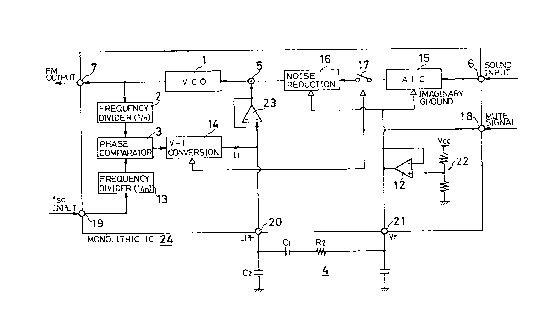
Fig. 1 shows one embodiment in accordance with the
present invention, which is embodied in an integrated
circuit comprising such a circuit for producing a
reference potential. In Fig. 1, the reference numeral 1
denotes a VCO (voltage-controlled oscillating) which
serves as a frequency modulation circuit, the reference
- 2Q2S6~ft
numeral 2 denotes a l/n frequency divider, the reference
numeral 3 denotes a phase comparator, and the reference
numeral 4 denotes a loop filter. A PLL is so constructed
as to include the VCO 1 and the loop filter 4 including
capacitors Cl and C2 and resistors Rl and R2.
The the reference numeral 5 denotes an adding
circuit, the reference numeral 6 denotes an input
terminal for a sound signal, and the reference numeral 7
denotes an output terminal of a frequency-modulated
signal.
The reference numeral 12 denotes a voltage follower
which serves as a reference voltage source as described
above, the reference numeral 13 denotes a l/m frequency
divider, and the reference numeral 14 denotes a V-I
(voltage-current) conversion circuit which serves as a
current source Il shown in Figs. 8 and 9, which charges
the capacitor Cl of the loop filter 4.
The reference numeral 15 denotes an ALC circuit
which controls a le-~el of an inputted sound signal at
constant, the reference numeral 16 denotes a noise
reduction (NR) circuit, the reference numeral 17 denotes
a switching means for muting the sound signal, the
reference numeral 18 denotes an input terminal for a mute
signal, the reference numeral 19 denotes an input
terminal for a signal fsc (a color sub-carrier frequency
-- 10 --
- 2~25 6~ ~9
signal) which serves as a frequency reference signal, the
reference numerals 20 and 21 denote connection terminals
for external components of the loop filter 4, and the
reference numeral 22 denotes a voltage divider for the
voltage follower 12.
In addition, the reference numeral 23 denotes a
voltage follower and the reference numeral 24 denotes a
monolithic IC which incorporates the above described
components 1-3 and 5-23 except for the loop filter 4.
In Fig. 1 embodiment, a sound signal inputted to
the terminal 6 is supplied to the VCO 1 through the ALC
circuit 15 and NR circuit 16 to control an oscillation
frequency of the VCO 1, whereby a frequency modulation is
performed. A frequency modulated sound signal is given
to the phase comparator 3 after the same is frequency-
divided at l/n in the frequency divider 2. On the other
hand, the fsc signal which is an output of a crystal
oscillating circuit (not shown) and serves as a frequency
reference signal is given to the phase comparator 3 after
the same is frequency-divided at l/m in the frequency
divider 13. In addition, a center frequency signal of
the VCO 1 which is frequency-divided at l/n is so set as
to become the same frequency as that of the fsc signal
which is frequency-divided at l/m.
An output of the phase comparator 3 is converted
202S60~
into a current value by the V-I conversion circuit 14 to
be supplied to the external capacitor Cl and etc. through
the terminal 20 so that only very low frequency
components which exist outside the frequency band of the
sound signal can be remained, being given to the adding
circuit 5 through the voltage follower 23. That is, a
variation having nothing to do with the inputted sound
signal of the oscillation frequency of the VCO 1, which
may be a variation of the center frequency, is so
controlled as to be stabilized at a predetermined value
by a PLL operation according to the phase comparison with
the reference signal, whereby no adjustment become to be
required.
Meanwhile, in the above described circuit, since an
objective signal to be processed is a sound signal, in
order to prevent the PLL operation from being influenced
by the sound signal, as described above, a time constant
of the loop filter is made very large. Therefore, at a
timing when the power source of an integrated circuit 24
is turned-on, a voltage which determines a center
frequency of the VCO 1 is zero volt. in Fig. 6 circuit
configuration, and therefore, it takes a long time until
the voltage rises up to a predetermined voltage. That
is, it takes a lot of time until the center frequency of
the frequency modulation circuit 1, i.e. a frequency
202560~
which is not frequency-modulated becomes a correct value.
In order to prevent such a problem, in Fig. 1
circuit configuration, the reference voltage Vr(=Vcc/2)
is supplied to the external capacitor Cl. The voltage Vr
rises in the same manner as that of the power source
voltage Vcc, and therefore, when the power source voltage
Vcc reaches to a value of the steady state, the voltage
Vr becomes a value of Vcc/2. Therefore, in turning the
power source on, the voltage of Vcc/2 is rapidly given to
the capacitor Cl to be utilized as a voltage for
controlling a center frequency of the VCO 1.
Accordingly, the voltage of the terminal 20 rises in the
same way of the rising of the power source voltage, and
therefore, the oscillation frequency can be rapidly
controlled to a nominal center frequency.
In addition, in the PLL circuit or the like,
normally, a voltage applied to the VCO in a phase-locked
state is set as Vcc/2, and therefore, the voltage of the
terminal 20 in a state where the circuit is actually
operated is a value nearly equal to Vcc/2. Therefore, by
setting the voltage Vr at Vcc/2 in a steady state, that
is, by setting the voltage for biasing the capacitor Cl
of the loop filter at a control voltage of a phase-locked
state of the PLL, the center frequency of the VCO 1 can
be rapidly set.
20256~B
,
In addition, the voltage Vr is also supplied to the
ALC circuit 15 and the NR circuit 16.
Furthermore, in Fig. 1 circuit configuration, the
pull-in of the center frequency can be made rapidly by
using the mute signal. More specifically, in response to
the mute signal which controls the switching means 17, a
time constant of the loop filter 4 is made small
substantially. To that end, the mute signal is supplied
to the current source 14 to make an output current (Il or
-Il) of the current source larger than that of the steady
state, resultingly, a time required to charge or
discharge is shortened. That by which this point is
represented in detail is Fig. 2.
In Fig. 2, the same reference symbols are applied
to the same or similar components of Fig. 1, and
therefore, a description will be omitted here. In
addition, since respective components are well known in
an integrated circuit, a description thereof will be also
omitted. When the mute signal is in an active state (the
low level), an emitter current of a differential pair
provided at a front stage of the V-I conversion circuit
14 is set so as to become a value of approximately ten
times an emitter current in a state where no muting
operation is performed (lOIl). Therefore, a current
amount flowing out from the terminal 20 or flowing into
202~5Q~
the terminal 20 in the muting period becomes
approximately ten times a current amount in the steady
state. Accordingly, a time required to charge or
discharge the capacitor which is connected to the
terminal 20 become short, and thus, the time constant of
the loop filter 4 is equivalently made small.
The mute signal is a signal which is produced when
the power source is turned-on or when an operation mode
is changed from a play mode to a stop mode. When the mute
signal is in an active state, the switching means 17 is
turned-off in Fig. 1 circuit. The mute signal produced
in turning the power source on is generated so that the
same is the low level for a predetermined time period in
response to the turning-on of the power source.
When no reference voltage source is provided in an
integrated circuit, it is possible to utilize a circuit
configuration shown in Fig. 10. In Fig. 10 circuit
configuration, the power source voltage Vcc is utilized
for a bias voltage for biasing the capacitor Cl of the
loop filter 4. More specifically, a voltage divided by
the resistors R2a and R2b becomes the bias voltage. In
addition, since the power source and the ground have the
same level in an alternating current, a resistance value
of a parallel circuit of the resistors R2a and R2b must
be set to be equal to a resistance value R2.
- 202~
Although the present invention has been described
and illustrated in detail, it is clearly understood that
the same is by way of illustration and example only and
is not to be taken by way of limitation, the spirit and
scope of the present invention being limited only by the
terms of the appended claims.
- 16 -