Note: Descriptions are shown in the official language in which they were submitted.
20~7~
1 BACKGROUND OF THE INVENTION
The present invention relates to an information
processor using a disk memory having a disk for use in a
portable recording medium capable of reading, writing,
erasing, and/or overwriting in a thin rectangular card and
a disk memory used therein.
A card which performs read/write of information
while rotating a recording medium such as an optical disk
and a floppy disk using a tellurium alloy in a flat space
is described in JP-A-60-79581.
A magneto-optical disk memory device capable of
overwriting by laser power modulation is described in
JP-A-62-175948, but a permanent magnet for initializing a
magneto-optical disk and a permanent magnet for writing
lS are fixed to an optical disk memory device, and further-
more, an optical head is positioned on an opposite side to
the magneto-optical disk. Moreover, in the magneto-
optical disk, such a method is adopted that an optical
disk medium is fixedly adhered onto a substrate having a
thickness of approximately 1.2 mm so as to have light
incident from the substrate side as a countermeasure
against dust attaching thereto, and the optical disk is
contained in a protective case for transportation, thus,
requiring a thickness of 6 to 10 mm as the whole optical
disk. Because of the fact that the substrate requires to
- 1 - *
~2~72~
1 have a thickness of 1.2 mm and the permanent magnet for
initialization and the permanent magnet for recording are
fixed on the opposite side with respect to the optical
head and the optical disk in a conventional magneto-
optical disk as described above, the thickness of thispermanent magnet portion is added, thus not only causing
it difficult to miniaturize the optical disk, in
particular to form it in a credit card ordered size, but
also limiting to form a thin optical disk memory device.
On the other hand, an example in which a disk
magneto-optical medium capable of overwriting on a glass
substrate having a thickness of 1.2 mm is incorporated in
a cartridge, a permanent magnet for application of
initializing auxiliary magnetic field is incorporated in
the cartridge, and a permanent magnet for recording is
installed in a recording device is disclosed in JP-A-
64-46247. However, it is difficult to miniaturize and
thin an optical disk, in particular to form it in a credit
card ordered size when the cartridge is included because
the thickness of 1.2 mm is required for the substrate.
Further, since the permanent magnet for recording is fixed
on the opposite side with respect to the optical head and
the optical disk, the thickness of this permanent magnet
portion is added, and thus, there has been a limit to make
the optical disk memory device thinner. Moreover, there
is also such a problem that the laser portion of the
optical disk is liable to be damaged because the optical
disk is exposed when the window of the cartridge cover is
I opened. 232~724
When a disk capable of reading, writing, erasing,
and/or overwriting by a laser power modulation is used as a
memory for a lap top computer or other portable information
processors, it is desirable to be rectangular in configuration
and to be in a card form or a sheet form in point of thickness
which is provided with a protective case from the viewpoint of
portability. In a conventional optical disk, however, because
of such a fact that the substrate requires a thickness of 1.2
mm as a counter-measure against sticking dust, and
particularly in the case of magneto-optical recording, the
permanent magnet for initialization and the permanent magnet
for recording are fixed on the opposite side of the optical
disk with respect to the optical head. Thus, the thickness of
this permanent magnet portion is added, which creates a limit
to form a thin film, and it has been impossible to use such a
conventional optical disk in a lap top computer and a portable
optical disk memory device.
SUMM~RY OF THE INVENTION
The present invention consists of a magneto-optical
disk medium comprising: (a) a disk shaped magneto-optical
recording medium comprising a transparent substrate and a
recording layer for recording, reproducing and writing
information by laser power and magnetic field, and (b) a
protective case in which said recording medium is mounted
rotatably so as to form a narrow gap between a surface of the
recording medium and an inside surface of the protective case
for maintaining the recording medium substantially in parallel
therewith and limiting the recording medium against rotational
- 3 -
2025 724
fluctuation, and said case having a window for irradiating a
laser beam onto said recording layer through said transparent
substrate, and wherein the total of the thickness of said
transparent substrate and of said case at the light incident
window is equal to or less than approximately 1.2 mm.
The disk may be contained in a case of credit card
size, which is convenient for transportation.
An information processor of the present invention
comprises a magneto-optical disk as described above and an
optical head for recording information on the recording
medium.
BRIEF DESCRIPTION OF THE DRAWINGS
Fig. 1 is a block diagram showing a device
composition of an embodiment of the present invention;
Fig. 2A is a plan view showing an embodiment of a
magneto-optical disk-in-card of the present inventioni
Fig. 2B is a sectional view taken along arrow marks
IIB-IIB in Fig. 2A;
Fig. 2C is a sectional view taken along arrow marks
IIC-IIC in Fig. 2A;
Fig. 2D is an enlarged sectional view of the section
shown in Fig. 2C;
Fig. 3 is a sectional view showing another
embodiment of Fig. 2D;
Fig. 4 is a plan view showing an optical disk-in-
card;
Fig. 5A is a plan view showing an optical disk in
the optical disk-in-card;
- 4 -
2~572~
1 Fig. 5B is a sectional view taken along arrow
marks VB-VB in Fig. 5A;
Fig. 6 is a sectional view of a magneto-optical
disk;
Fig. 7 is an enlarged sectional view showing an
optical disk-in-card;
Fig. 8 is an enlarged sectional view showing
another embodiment of the optical disk-in-card;
Fig. 9 is an explanatory diagram of principles
of write/read/erase of a phase-change optical disk;
Fig. 10 is a diagram showing a crystallizing
speed of an In-Sb-Te write medium which is an example of a
material for a phase-change optical disk;
Fig. 11 and Fig. 12 are sectional views showing
a multilayer film composition of the optical disk;
Fig. 13 is an explanatory view of a modulation
method of laser power;
Fig. 14A is a composition diagram showing an
embodiment of an optical head for a phase-change optical
disk;
Fig. 14B is a side view of the optical head
shown in Fig. 14A;
Fig. 15 is a composition diagram showing still
another embodiment of the optical head for a magneto-
optical disk;
Fig. 16 is an explanatory diagram of principles
of initialization, write, read and overwrite of a magneto-
optical disk;
~/
2(~25~4
Fig. 17 and Fig. 18 are sectional views showing
multilayer compositions of the magneto-optical disk;
Fig. 19 is a block diagram showing an embodiment
of a drive circuit system;
Fig. 20 iS a plan view showing another magneto-
optical disk-in-card;
Fig. 21A iS a plan view showing another embodi-
ment of the optical disk-in-card;
Fig. 21B and Fig. 21C are respective side views
of the optical disk-in-card shown in Fig. 21A;
Fig. 22A is a sectional view of an optical
disk-in-card taken along arrow marks XXIC-XXIC in Fig. 21A;
Fig. 22B iS an enlarged sectional view shown
with an arrow mark F in Fig. 22A;
Fig. 22C is an enlarged sectional view shown
with an arrow mark G in Fig. 22A;
Fig. 23A iS a plan view of another optical disk;
Fig. 23B is a sectional view taken along arrow
marks XXIIIB-XXIIIB in Fig. 23A;
Fig. 24 and Fig. 25 are sectional views showing
examples in which countermeasures of preventing mixing of
dust and dirt into recording areas of the optical disk;
Fig. 26A is a plan view showing another embodi-
ment of an optical disk-in-card;
Fig. 26B thru Fig. 26D are respective side views
of the optical disk-in-card shown in Fig. 26A;
Fig. 27 iS a plan view showing another embodi-
ment of a magneto-optical disk-in-card;
l,
2625~24
1 Fig. 28A is a plan view showing still another
embodiment of the optical disk-in-card;
Fig. 28B and Fig. 28C are respective side views
of the magneto-optical disk-in-card shown in Fig. 28A;
Fig. 29A is a sectional view taken along arrow
marks XXVIIIC-XXVIIIC shown in Fig. 28A;
Fig. 29B is an enlarged sectional view shown
with an arrow mark K in Fig. 29A;
Fig. 29C is an enlarged sectional view shown
with an arrow mark L in Fig. 29A;
Fig. 30 and Fig. 31 are sectional views showing
another examples in which countermeasures for preventing
mixing of dust and dirt into the recording area of an
optical disk are taken;
Fig. 32A is a plan view showing another embodi-
ment of an optical disk-in-card;
Fig. 32B thru Fig. 32D are respective side views
of the optical disk-in-card shown in Fig. 32A;
Fig. 33 is a block diagram showing a composition
in case, the optical disk-in-card is applied to a lap top
computer;
Fig. 34 is a block diagram showing a composition
in case, the optical disk-in-card is applied to a camera;
Fig. 35 is a block diagram showing a composition
in case, the optical disk-in-card in applied as a memory
for a terminal of a large computer and an interface of a
lap top computer;
1,
2~2~7~
1 Fig. 36 is a plan view showing another embodi-
ment of the optical disk-in-card;
Fig. 37 is a block diagram showing another
device composition of the present invention;
Fig. 38 is a plan view showing another embodi-
ment of the optical disk-in-card;
Fig. 39A is a plan view showing still another
embodiment of the optical disk-in-card;
Fig. 39B is a sectional view taken along arrow
marks XXXIXB-XXXIXB in Fig. 39A;
Fig. 40A is a plan view showing another embodi-
ment of the optical disk-in-card;
Fig. 40B and Fig. 40C are respective side views
of the optical disk-in-card shown in Fig. 40A;
Fig. 41 is a plan view showing another embodi-
ment of the optical disk-in-card;
Fig. 42A is a plan view showing still another
embodiment of the optical disk-in-card;
Fig. 42B is a sectional view taken along arrow
marks XLIIB-XLIIB in Fig. 42A;
Fig. 43A is a plan view showing another embodi-
ment of the optical disk-in-card; and
Fig. 43B and Fig. 43C are respective side views
of the magneto-optical disk-in-card shown in Fig. 43A.
DETAILED DESCRIPTION OF THE EMBODIMENTS
An embodiment of the present invention will be
described hereafter with reference to drawings. Fig. 1
~2~72~
1 shows a conceptual diagram of an information processor of
the present invention.
The information processor of the present
invention is composed of an optical disk-in-card 100
consisting of a transparent protective case 120 housing at
least one recording layer of a rotatable disk type optical
disk memory 140 of a recording layer, an optical disk
drive, a processor 400, an input means 500 and an output
means 600.
The magneto-optical disk-in-card 100 incorpo-
rated in a transparent protective case is composed of a
transparent protective case 120 housing a magneto-optical
disk memory 140, a first magnetic field application means
for initializing an auxiliary recording layer and a second
magnetic field application means for recording information
a recording layer, and is detachable from the disk drive
200.
Furthermore, an optical disk memory such as a
phase-change type, write-once type, and/or read-only type
may also be used in place of the magneto-optical disk
memory 140. In this case, the optical disk is incorpo-
rated in a transparent protective case is composed of an
optical disk and a transparent protective case.
Further, the disk drive 200 is composed of an
optical head 210 for write, read and overwrite, a motor
240 for rotating the optical disk 140 and a drive circuit
260 for controlling the optical head 210 and the motor
240. The optical head 210 is provided with an objective
q~
B ---
~2~72~
1 lens 219 for irradiating the optical disk 140 with light.
The drive circuit 260 controls the rotation
speed of the motor 240 and also fulfils functions of
modulation of data for write/overwrite and demodulation of
data for read in accordance with an instruction from the
processor 400.
Further, the processor 400 performs arithmetic
processing or write/read in and from the magneto-optical
disk 140 in accordance with an instructions from the input
means 500, and outputs the written information in the
magneto-optical disk 140 or processing results through the
output means 600.
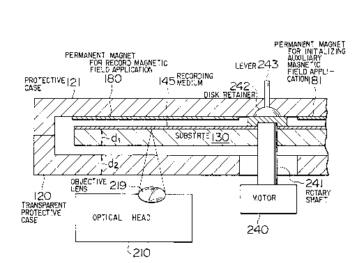
Fig. 2A, Fig. 2B, Fig. 2C and Fig. 2D show an
embodiment of the magneto-optical disk-in-card incorpo-
rated in a transparent protective case best suited forexecuting the present invention. Besides, the optical
head 210 and the motor 240 for rotating the optical disk
140 are shown additionally in the detailed portion of the
magneto-optical disk-in-card. At the terminal portion of
a rotary shaft 241 extending from the motor 240, a disk
retainer 242 and a level 243 are provided so as to fix the
optical disk 140.
As shown in respective figures, the magneto-
optical disk 140 is incorporated in a protective case 120,
121 of a credit card size in the magneto-optical disk-in-
card 100 of the present embodiment. A permanent magnet
180 for magnetic field application for initializing the
auxiliary recording layer and a permanent magnet 181 for
~ la,
~02~72~
1 magnetic field application for writing in the recording
layer are formed on the disk in the transparent protective
case 121. It is better for the permanent magnet for
magnetic field application for initialization and the
permanent magnet for magnetic field application for
recording to be fixed both at a length a little longer
than the radial length of the recording area of the
magneto-optical disk of the magneto-optical disk memory
card because initialization and writing can be executed up
to the innermost periphery or the outermost periphery of
the disk. Further, configurations of the permanent magnet
for magnetic field application for initialization and the
permanent magnet for magnetic field application for
recording may be rectangular when the rotation speed of
the disk is as low as 1,800 rpm. When the rotation of the
disk reaches 3,600 rpm and higher, it is more preferable
to form the configurations of the permanent magnet for
magnetic field application for initialization and the
permanent magnet for magnetic field application for
writing in sectors so that the circuit arc is small at the
inner periphery of the disk and the circular arc is large
at the outer periphery of the disk for initialization and
writing. The manufacture of the permanent magnet for
magnetic field application for initialization and the
permanent magnet for magnetic field application for
writing may be made by cutting out of a bulk material and
adhering with adhesives, or by any of thin film forming
methods such as a vacuum deposition method, a sputtering
2~2~7~4
1 method and an ion beam sputtering method.
At least a light beam incident portion 152 of
the protective case is composed of a transparent plate in
the magneto-optical disk 140.
In a conventional magneto-optical disk unit, a
window of the protective case was opened so that light is
directly incident to an optical disk when light was
incident. Therefore, dust and dirt entered through the
window for light incidence, and it was required to use a
transparent substrate having a thickness of 1.2 mm for the
substrate as a countermeasure thereagainst.
On the contrary, since the light incident
portion 152 is covered with the transparent protective
plate 120 in the magneto-optical disk-in-card of the
present invention, dust and dirt will never stick directly
to the optical disk. Accordingly, the substrate for
supporting the optical disk medium needs not have the
thickness of 1.2 mm. According to the present invention,
dust in air does not stick to a substrate 130 and a
reading medium 145 consisting of an auxiliary recording
layer and recording layer, thus producing an effect that
the substrate having a thickness of 1.2 mm which has been
heretofore deemed indispensable may be made thinner by
forming the total of the plate thickness d2 of the trans-
parent protective case 120 and the plate thickness dl ofthe substrate 130 in approximately 1.2 mm.
Fig. 3 shows another embodiment in place of Fig.
2D. When the thickness d2 of the transparent protective
B - '
2 02~ 724
1 plate is made at approximately 1.2 mm, it is not required
to have light incident from the substrate 130 side, thus
making it possible to use for the substrate 130 a metal, a
metallic foil and an organic material having no light
permeability such as an aluminum foil made thinner by cold
processing and an alloy foil thereof, a stainless steel
foil, and a titanium foil or an alloy foil thereof.
Further, the magneto-optical disk is fixed to
the rotary shaft 241 and rotated, but is retained by the
disk retainer 242 for stable rotation. Besides, the
protective case 121 having no light incident portion, it
may be either transparent or opaque.
Moreover, in the magneto-optical disk-in-card of
the resent invention, the magneto-optical disk 140 is not
fixedly attached to the protective case 120, 121, but is
made rotatable freely.
Fig. 4 shows an embodiment of an optical disk
memory such as a phase-change type, write-once type,
and/or read-only type contained in a transparent
protective case (hereafter referred to as an "optical
disk-in-card") best suited to realize an optical disk
memory of the present invention, and the section of this
figure is the same as Fig. 2C. Referring to Fig. 2C, the
optical disk 140 incorporated in the protective case 120,
121 each in a card in a card size in the optical disk-in-
card 100. Here, at least the light beam incident portion
152 of the protective case is formed of a transparent
protective plate in the optical disk 140.
13,
~02~724
1 In a conventional optical disk unit, the window
of the protective case was also opened like a magneto-
optical disk unit so as to have light incident directly to
the optical disk when light was incident. Therefore,
since dust and dirt entered through the window for light
incidence, it has been required to use a transparent
substrate having a thickness of 1.2 mm for the substrate
as a countermeasure.
On the contrary, since the light incident
portion 152 is covered with the transparent protective
plate 120 in the optical disk memory of the present
invention, dust and dirt will never stick directly to the
optical disk, thus the thickness of the substrate for
supporting the optical disk medium needs not be 1.2 mm.
Further, in the optical disk memory of the
present invention, the optical disk 140 is not fixedly
attached to the protective case 120, but is made rotatable
freely.
Fig. 5A and Fig. 5B show an embodiment of an
optical disk in the optical disk-in-card 100. The optical
disk 140 is formed of a substrate 143 and a recording
medium 145. In these figures, a indicates a recording
area and b indicates a non-recording area.
Here, the memory capacity for an optical disk-
in-card is estimated. In the field of an IC card and a
memory card, the outside dimension of a card has been
already standardized, and the overall size is approxi-
mately 54 mm x 86 mm.
202~72~
1 In the optical disk-in-card 100 of the present
invention, it is preferable that the size of the
protective case is also substantially in accordance with
the size of the card in order to be used as a portable
memory.
Thereupon, the memory capacity is estimated here
assuming that a protective case having the overall size of
54 mm x 86 mm is used. Since the breadth is 54 mm, it is
preferable that the outside dimension of the optical disk
is 50 mm and less when 1 mm is assigned to edges, respec-
tively. Further, since it is preferable that the record-
ing area a in the optical disk is located about 1 mm
inside the overall size of the disk, the outside diameter
of the recording area a is preferably at approximately 48
mm.
On the other hand, the inside diameter of the
recording area a is determined depending on the sizes of
hub fitting for disk rotation and the disk retainer
portion. Since about 15 to 28 mm is sufficient for the
disk retainer portion, it may be concluded that 15 mm to
48 mm may be used as the recording area. When the outside
dimension of the recording area is given, the memory
capacity reaches the maximum when he inside diameter is
selected at half of the outside dimension.
Thereupon the memory capacity when 24 mm to 48
mm is used as the recording area is estimated here. When
an ordinary optical disk system is used, 1.6 ~m is
adopted as the spacing between tracks. Therefore, 7,500
~,
B - -
7 2 ~
1 tracks are obtained when the number of tracks are
estimated with the above. Besides, since the bit density
is at approximately 1.4 ~m/bit, the number of bits per
track is obtained at approximately 53.8 Kbits per track.
Accordingly, a recording capacity of approxi-
mately 50 MB (mega bytes) is obtainable at the time of
unformat for the whole recording area.
Fig. 6 shows an embodiment of an magneto-optical
disk in the magneto-optical disk-in-card 100. The
magneto-optical disk 140 is composed of the recording
medium 145 consisting of the substrate 130, the auxiliary
recording layer and the recording layer. Fig. 6 is a
partial sectional view showing another embodiment of the
magneto-optical disk 140 shown in Fig. 5A. When light is
incident from the substrate 130 side as shown in Fig. 2D,
the substrate 130 needs to be transparent with respect to
the wavelength of light employed. Among recording media,
145-1 becomes the write layer and 145-2 becomes the
auxiliary recording layer. Further, 145-1 becomes the
auxiliary recording layer and 145-2 becomes the recording
layer among recording medium when light is incident from
the side of the recording medium 145 as shown in Fig. 3.
In the case of the latter, the substrate 130 may be either
transparent or opaque.
Here, the capacity, etc. of the memory for the
magneto-optical disk-in-card is substantially similar to
that of the memory for the optical disk-in-card.
That is, it becomes possible to make an optical
2~2~72~
1 or magneto-optical disk-in-card thinner, and in its turn
to make an information processor such as a lap top
computer thinner.
Fig. 7 and Fig. 8 are for explaining the concept
of the present invention using an optical disk-in-card,
and correspond to Fig. 2D and Fig. 3. With this, it
becomes possible to make the optical disk thinner, and in
its turn to make an information processor such as a lap
top computer thinner.
As shown in Fig. 7, the present invention is
composed of the substrate 130 supporting the recording
medium 145, a protective case 120, 121 for protecting
them, the motor 240 for rotating a disk and the optical
head 210. The optical head may be realized essentially
with an optical system as described in Nikkei Electronics,
Nov. 21, 1983, pp. 189 - 213.
Write/read/erase of the optical disk are
implemented with such a composition as follows. That is,
new information is recorded on old information by modulat-
ing the power of a semiconductor laser in the optical head210 between an erasing power and a writing power at the
time of write/erase.
Further, the reflectance of the optical disk is
read by contracting the semiconductor laser power to a
comparatively small power and radiating it continuously at
the time of reading. Here, a feature of the present
invention exists in that a laser beam is radiated to the
recording medium 145 through the transparent protective
2 ~
1 case 120.
That is, according to the present invention,
there is such an effect that dust in air will never stick
to the substrate 130 and the recording medium 145, and the
substrate having a thickness of 1.2 mm which has been
heretofore deemed indispensable may be made thinner by
making the total of the plate thickness d2 of the
transparent protective case 120 and the plate thickness
dl of the substrate 130 approximately 1.2 mm.
Similarly, when the thickness d2 of the
transparent protective plate of the present invention is
made to be approximately 1.2 mm as shown in Fig. 8, it is
not necessary to have light incident from the substrate
130 side, then a material having no light permeability can
be used for the substrate 130. Further, the optical disk
is fixed to the rotary shaft 241 and rotated, but is
retained by the disk retainer 242 for stable rotation.
Furthermore, since the protective case 121 is not a light
incident portion, it may be either transparent or opaque.
Next, a recording medium best suited to realize
the present invention will be explained. As the recording
medium, a read-only medium such as a compact disk, a write
once optical recording medium utilizing hole boring and
phase-change, and a reversible optical read medium utiliz-
ing magneto-optical effect and phase-change may be used.
That is, any medium which is able to read or write/erase
by means of a laser beam may be used as a medium in the
present invention.
B~
2~)2~72~
1 Here, an example of write/erase/read utilizing a
reversible phase-change optical disk will be explained.
Fig. 9 shows principles of write/erase/read of a phase-
change optical disk. As shown in the figure, writing is
realized by irradiating a recording medium with a laser
beam of comparatively high power and quenching a recording
film 142 after melting, thereby to bring the recording
film 142 under amorphous state. On the other hand,
erasing is realized by irradiating the recording film 142
with a laser beam of comparatively low power and bringing
the recording film 142 in amorphous state under a
crystallized state. Further, reading is performed in such
a manner that the recording medium is irradiated with
continuous light of further lower power, thereby to read
information by the difference between reflection factors
under amorphous and crystallized states.
Any phase-change medium such as an In-Sb-Te
recording film described in Proc. Soc. Photo-Opt. Inst.
Eng. (SPIE), Vol. 1078, pp. 11 - 26, (1989) or a recording
film capable of overwrite described in Proc. Soc. Photo-
Opt. Inst. Eng. (SPIE), Vol. 1078, pp. 27 - 34, (1989) may
be used as the recording film 142.
Fig. 10 shows the crystallization time of an
In-Sb-Te material, but this recording film 142 has
different crystallization times depending on the composi-
tion of the material and has a crystallization time
ranging from 50 ns to 500 ns. Although there is a
~ Iq~
2~2~72~
1 variation to some extent in selecting which crystalli-
zation time to be adopted depending on a linear velocity
v(m/s) of the optical disk and a film structure of the
optical disk medium, it is preferable to adopt a recording
film having a crystallization time in the range of
approximately from 500/v ns to 1,500/v ns.
Further, Fig. 11 shows a film structure best
suited to be used for the optical disk medium shown in
Fig. 7. The optical disk medium is composed of a light
permeable substrate 130, a first light interference film
141 having a high refractive index characteristic, a
recording film 142, a second light interference film 143
having a high refractive index characteristic, a
reflecting film 144 and a protective film 145a. In such
an optical disk medium, light is incident from the
substrate side.
On the other hand, Fig. 12 shows a film
structure best suited to be used as the optical disk
medium shown in Fig. 8. In this case, a feature exists in
that the order from the first light interference film 141
to the reflecting film 144 is reversed because the laser
beam is incident from the protective film. Here, the
interference film fulfils the functions of improvement of
contrast by light interference and a control film of heat
conduction characteristic.
Fig. 13 shows a modulation method of the laser
power at the time of overwriting. That is, the laser
power is modulated between the power level for erasing and
.~, ~,
202~724
the power level for recording at the time of overwriting.
At this time, the laser power for erasing is selected from
the power which is able to crystallize the recording film
when this power is continued to be radiated, and the power
5 for recording is selected from the power which is able to
bring the recording film under amorphous state.
Fig. 14A and Fig. 14B show an example of the
optical head 210 best suited to execute the present
invention. In a conventional optical head, an actuator
10 for driving an objective lens was provided for focal point
control, but it was difficult to make the optical head
thinner because of this actuator. In the optical head 210
of the present invention, the actuator for the objective
lens 219 is deleted, and a relay lens 216 is provided
15 instead and moved in a parallel direction with the disk,
thereby to realize focal point control. Further, aberra-
tion on a disk is compensated in an ordinary objective
lens by utilizing a plurality of lenses, but a part
thereof is split and moved to the whole surface of a riser
20 mirror 218 so as to make the optical head thinner.
The optical head 210 shown in Fig. 14A will be
described. Luminous flux emitted from a semiconductor
laser 211 passes through a collimator lens 212 and a
shaping prism 213, and the luminous flux is reflected by a
25 polarizing prism 214. The reflected luminous flux passes
through a condenser lens 220 for detection, and is
detected by an optical sensor 221. The luminous flux
which has passed through the polarizing prism 214 passes
~1/
202~7~
1 through a ~/4 plate 215 and is converged appropriately
by a relay lens 216 having a focus actuator 230, and then
passes through an objective lens 217 and is reflected by a
riser mirror 218, and is radiated onto the optical disk
thereafter through an objective lens 219. The optical
head 210 shown in Fig. 14B includes the optical sensor 221
provided with light permeability in place of the
polarizing prism 214 and a relay lens 216 provided with no
focus actuator 230.
In Fig. 2A, Fig. 2B, Fig. 2C, Fig. 2D and Fig.
3, the optical head 210 may be realized with the optical
system shown in Fig. 15. A divergent luminous flux
emitted from a semiconductor laser 211 passes through a
beam splitter (hereafter abbreviated as BS) 232 through a
~/2 plate 231-1 and a collimator lens 212 and becomes
parallel luminous fluxes. The parallel luminous fluxes
are reflected further by the riser mirror 218, and
converted thereafter into parallel fluxes again by the
objective lens 219 and radiated onto the optical disk
140. On the other hand, the luminous flux passes through
a ~/2 plate 231-2 after reflected ~y the BS 232, and is
incident to a detection lens 220 consisting of a combi-
nation of a convex lens and a concave lens so as to become
a convergent luminous flux. The convergent luminous flux
is incident to a cylindrical lens 233, thus producing
astigmatism. The luminous flux which has passed the
cylindrical lens 233 is incident to a micro BPS 234 which
is an analyzer. This micro BPS 234 is composed of a
20257 2A
1 parallelogram prism and transparent parallel flat plates
putting a polarizing film which transmits P-polarized
light (polarized light in a vibration direction parallel
with the paper surface) and reflects S-polarized light
(polarized light in a vibration direction perpendicular to
the paper surface) therebetween. The convergent luminous
flux is incident to the polarizing film from the upper
side of the parallelogram prism. The P-polarized light
which has transmitted through the polarizing film is
totally reflected by the back plane of the parallel flat
plates and passes through the polarizing film again, and
then advances toward the left side of the parallelogram
prism. On the other hand, the S-polarized light reflected
by the polarizing film also advances in the same direction
as the P-polarized light, and is incident to the optical
sensor 221 at a certain interval. This interval is
controlled by means of the parallel flat plates.
Fig. 16 shows the principle of overwriting a
magneto-optical disk by laser power modulation. A write
medium best suited for realizing the present invention
will be explained with this principle. As shown in Fig.
6, the optical recording medium has a two-layer structure
of the recording layer and the auxiliary recording layer,
in which the recording layer on the side applied with a
laser beam is composed of TbFe which has a large coercive
force Hc and a low curie temperature and the auxiliary
recording layer is composed of GdTbFe which has a small
coercive force Hc and a high curie temperature. Besides,
B ~
2~2~24
1 the permanent magnet for applying initializing auxiliary
magnetic field is made to generate a magnetic field
stronger than that of the permanent magnet for applying
recording magnetic field. First, magnetization of the
auxiliary recording layer having small Hc is oriented in a
magnetizing direction in the permanent magnet for applying
initializing auxiliary magnetic field. At this time,
since magnetization of the recording layer has coercive
force larger than that of the permanent magnet for
applying initializing auxiliary magnetic field, the
magnetizing direction is not reversed. When the recording
medium reaches a position where the laser beam is applied
under abovementioned state, magnetization of the auxiliary
recording layer having a high curie temperature is
preserved as is and only the recording layer reaches the
curie temperature and higher when the laser power is
weak. Thus, the magnetization of the recording layer is
oriented in the magnetizing direction of the auxiliary
recording layer in the cooling process. On the other
hand, since the auxiliary recording layer also reaches the
curie temperature when the laser power is strong, the
magnetization thereof is oriented in the direction of the
magnetic field of the permanent magnet for applying
recording magnetic field along with the recording layer.
That is, since the magnetizing direction is determined by
the difference in the intensity of the laser power, viz.,
modulation of the laser power, a process of erasing old
written contents becomes unnecessary, thus making
2~2~2 1
1 overwriting possible. Due to such a principle, it is
required that the permanent magnet for applying recording
magnetic field is positioned where the laser beam is
applied. However, the permanent magnet for applying
initializing auxiliary magnetic field needs not be placed
at positions shown in Fig. 2D and Fig. 3, but may be
placed at any position in the case on the recording area
of the magneto-optical disk which does not overlap with
the permanent magnet for applying recording magnetic field.
The optical recording medium is not limited to a
Tb21Fe79 recording layer and a Gd24Tb3Fe73
auxiliary recording layer so far as a two-layer structure
of a recording layer having a large coercive force Hc and
a low curie temperature and an auxiliary recording layer
having a small coercive force Hc and a high curie tempe-
rature is formed. Further, a composition of a GdTbFeCo
recording layer, a GdFeCo intermediate layer and a TbFeCo
auxiliary recording layer which is a two-layer lamination
having a third magnetic layer intermediately as a means
for reducing magnetic wall energy at the interface may be
used as well.
Since the permanent magnet such as SmCo and
NdFeB used as a second magnetic field application means
for recording in the recording layer is not transparent
with respect to the wavelength of incident light as seen
from the principle of overwriting, it is required that the
means for applying magnetic field for recording in the
recording layer is self-contained in a case on the
~5
:.`
2~724
1 opposite side of the light incident portion and the disk.
In Fig. 2D and Fig. 3, the first magnetic field applica-
tion means for initializing the auxiliary recording layer
is shown to be self-contained in the case on the opposite
side of the light incident portion and the disk, but the
first magnetic field application means for initializing
the auxiliary recording layer may be self-contained in the
case on the light incident side.
Fig. 17 shows a film structure best suited to be
used as a magneto-optical disk medium shown in Fig. 2D.
The magneto-optical disk medium is composed of a light
permeable substrate 130, a first light interference film
141 having a high refractive index characteristic, record-
ing layer 145-1, an auxiliary recording layer 145-2, a
second light interference film 143 having a high refrac-
tive index characteristic, a reflecting film 144 and a
- protective film 145a. In such an optical disk medium,
light is incident from the substrate side. Si2N4, AlN,
Ta2O5, ZnS and the like can be used as a dielectric film
having a high refractive index. An example of a manu-
facturing method and performance will be shown. First, a
first light interference film Si3N4 having a thickness
of 100 nm, then a recording film Tb20Fe80 having a
thickness of 100 nm, an auxiliary recording film
Gd24Tb5Fe71 having a thickness of 50 nm, a second
light interference film Si3N4 having a thickness of
100 nm and an Au reflecting film having a thickness of 100
nm have been formed by applying a sputtering method to a
2~2~72~
1 glass substrate having a thickness of 0.5 mm and a
diameter of 48 mm on which a groove having a depth of 100
nm and a pitch of 1.6 ~m is formed in a spiral form.
Furthermore, ultraviolet hardening resin having a thick-
ness of 100 ~m has been formed as a protective filmthereon. This magneto-optical disk was attached to the
transparent case shown in Fig. 2D, that is, a polycarbo-
nate substrate having a thickness of 0.6 mm obtained by
cutting a SmCo magnet having Hc at 40,000 e as the first
magnetic field application means for initializing the
auxiliary recording layer and a SmCo magnet 5 mm wide and
25 mm long having Hc at 3,000 e as the second magnetic
field application means for recording in the recording
layer out of a bulk. The performance of such a magneto-
optical disk-in-card has been evaluated. The disk-in-card
was rotated at the rotation speed of 3,600 rpm and tested
by the laser modulation method at the time of overwriting
shown in Fig. 13. That is, when 6.6 mW was set on the
write film surface as the bias power and 8.9 mW was set on
the recording film surface as the recording power and
overwrite test was executed while modulating the optical
beam between 2 MHz and 3 MHz, C/N was obtained at 54 dB
and the error generation factor was obtained at less than
10-5
On the other hand, Fig. 18 shows a film
structure best suited to be used as the magneto-optical
disk medium shown in Fig. 3. In this case, a feature
exists in that the order from the first light interference
2~25724
1 film 141 to the reflecting film 144 is reversed because
the laser beam is incident from the protective film.
Here, the interference film fulfils the functions of
improvement of contrast by means of interference of light
and the control film of heat conduction characteristic.
Besides, in this case, since the light incident side is
not on the substrate side, it is possible to form the same
film composition as that shown in Fig. 18 on the opposite
side of the substrate, thereby to use both sides of one
sheet of substrate. An example of a manufacturing method
and performance is shown. First, an Au reflecting film
having a thickness of 100 nm, a second light interference
film AlN having a thickness of 100 nm, an auxiliary
recording layer Tb24Fe65Coll having a thickness of 100 nm,
a recording film Gd24Tb3Fe73 having a thickness of 50 nm
and a first light interference film Si3N4 having a
thickness of 100 nm have been formed by applying a
sputtering method to a stainless steel substrate having
0.5 mm in thickness and 48 mm in diameter on which a
groove having 100 nm in depth and 1.6 ~m in pitch is
formed in a spiral form. Furthermore, ultraviolet
hardening resin having a thickness of 100 ~m has been
formed as a protective film thereon. This magneto-optical
disk was attached to the transparent case shown in Fig. 3,
that is, a polycarbonate substrate having a thickness of
0.6 mm obtained by cutting a SmCo magnet having Hc at
40,000 e as the first magnetic field application means for
initializing the auxiliary recording layer and a SmCo
2~2~'124
1 magnet 5 mm wide and 25 mm long having Hc at 3,000 e as
the second magnetic field application means for recording
in the recording layer out of a bulk. The performance of
such a magneto-optical disk-in-card has been evaluated.
When the disk-in-card was rotated at the rotation speed of
3,600 rpm, 6.6 mW was set on the recording film surface as
the bias power and 8.9 mW was set on the recording film
surface as the write power and overwrite test was executed
while modulating the optical beam between 2 MHz and 3 MHz,
C/N was obtained at 54 dB and the error generation factor
was obtained at less than 10 5.
An optical disk drive circuit system 260 is
explained in detail in Fig. 19. The optical disk drive
circuit system 260 is composed of a data management
portion 261, a track address control portion 262, a track
control portion 263, a focus control portion 264, a photo
detector and amplifier 265, a data demodulation portion
266, a data modulation portion 267, a laser drive 268 and
a motor control portion 269. With such a composition, at
the time of overwriting, a track address to be written is
determined in the track address control portion 262, and
the data modulation portion 267 converts the data given
from a processor 400 into "0" and "1" pattern to be
recorded on the optical disk by a modulation system. The
modulation system includes 2-7 modulation and 4-15
modulation, which, however, are used properly depending on
the system. In the laser drive 268, the laser power is
modulated between the bias power and the writing power as
B ~-
2~2~Z~
1 shown in Fig. 13 in accordance with the "0" and "1"
pattern determined by the data modulation portion 267.
Further, at the time of reading data, a track address
designated by the processor 400 is selected, the laser
power is set at a constant value of approximately 1 to 2
mW, the reflectance of the optical disk or the karr
rotation of the magneto-optical disk 140 is read by the
photo detector and amplifier 265, and the data are
demodulated by the data demodulation portion 266.
Further, the result of the photo detector and amplifier
265 may be utilized as the signal of the track control
portion 263 and the focus control portion 264, but the
functions of these portions can be realized with the
functions which have been heretofore employed in a compact
disk and an optical disk device. Further, the motor
control portion 269 controls the number of rotation of a
motor 240 for rotating the optical disk 140. There are
CAV (Constant Angular Velocity) type and CLV (Constant
Linear Velocity) type for the control of the number of
rotation.
In another embodiment of an optical or
magneto-optical disk-in-card of the present invention, a
means for rotating the disk is self-contained in the
card. With this, it is possible to make the thickness of
the whole information processor thinner by the portion of
the motor.
Fig. 20 shows another embodiment of the
disk-in-card 100. The basic composition is the same as
~2~72~
1 the composition shown in Fig. 4, and the light incident
portion is covered with a transparent protective case, but
the feature of the embodiment shown in Fig. 20 exists in
that a protective cover 160 is provided. Since the disk-
in-card 100 of the present invention is carried freely,
the card case 120 is flawed sometimes. There is no
problem even if other parts than the light incident
portion are flawed, but the card case needs to be replaced
sometimes if the light incident portion is flawed. It is
an object of the present invention to reduce the frequency
of replacement of the card case. That is, by providing
the protective cover 160 on the card case 120, it is
prevented that the light incident portion is flawed, and
incidence of light is made free by opening the protective
cover 160 when the optical disk-in-card is inserted into
the optical disk drive 200.
Fig. 21A, Fig. 21B and Fig. 21C show still
another embodiment of the optical disk-in-card 100.
Transparent protective plates 120 and 121 each have a film
thickness of approximately 0.5 to 1.2 mm and the optical
disk 140 (not shown) is inserted between these protective
plates 120 and 121. Further, 170 indicates a magnet clamp
for fixing the optical disk 140 to the rotary shaft for
rotating the optical disk. Fig. 22A is a sectional view
taken along arrow marks XXIC-XXIC shown in Fig. 21A, and
Fig. 22B and Fig. 22C are enlarged views shown with arrow
marks F and G shown in Fig. 22A. The optical disk 140 is
fixed with the magnet clamp 170 and is apart from the
~25~4
1 protective plates 120 and 121. Under the state that the
optical disk 140 is rotating, the optical disk 140 and the
substrate 130 are under floating states from the protec-
tive plates 120 and 121. Fig. 23A and Fig. 23B show an
example of the optical disk in this disk-in-card 100. The
central part of the disk is hollow in the example shown in
Fig. 5B, whereas the example shown in Fig. 23B has a
feature that the disk is fixed with the magnet clamp 170
at the central part thereof.
Fig. 24 is an enlarged view shown with an arrow
mark J in Fig. 23B and shows a preventive method against
mixing of dust and dirt into the recording area. Accord-
ing to the present invention, the light incident portion
is covered with a transparent protective cover. There-
fore, dust and dirt will never get directly into the
recording area, but the central part of the disk is open
for the purpose of rotation, thus it is possible that dust
and dirt mix in through this central part. Accordingly,
in the present invention, a dust protective mat 125 is
laid in a non-recording area so as to prevent mixing of
dust and dirt from the central part of the disk. An
example in which a magnet clamp is utilized was explained
with reference to Fig. 24, however, it is a matter of
course that this dust protective mat is applicable to the
example shown in Fig. 2.
Fig. 25 shows another example of a counter-
measure against dust corresponding to Fig. 24. In the
2 ~ 2 ~
1 example shown in Fig. 24, there was a fear that dust and
dirt mix in because the central part of the disk was
open. Whereas, the present embodiment has a feature that
a bearing 126 is provided at the central part of the disk
so as to delete the opened part.
Fig. 26A, Fig. 26B, Fig. 26C and Fig. 26D show
another embodiment related to the card configuration. In
above-described embodiment, a case that the card configu-
ration has an equivalent configuration to a credit card
has been described, but any configuration may be applied
so far as the size thereof may contain the optical disk.
Fig. 26A shows an embodiment of a substantially square
card having a protective cover 160. Besides, the size of
the optical disk has been shown at approximately 50 mm in
the present invention, but the size may be altered at
need. That is, the present invention is applicable to any
size such as 12 inches, 8 inches, 5.25 inches, 5 inches
and 3.5 inches which have been heretofore developed.
Fig. 27 shows another embodiment of the magneto-
optical disk-in-card 100 for realizing the present inven-
tion. The basic composition is the same as the composi-
tion shown in Fig. 2A and the light incident portion is
covered with a transparent protective case, but the
feature of the embodiment shown in Fig. 27 exists in that
a protective cover 160 is further provided. Besides, the
permanent magnet for initializing the auxiliary recording
layer of the recording medium and the permanent magnet for
recording in the recording layer are in the protective
B -33
2~23724
1 case. Since the magneto-optical disk-in-card 100 of the
present invention is carried freely, the card 120 is
flawed sometimes. There is no problem even if other parts
that the light incident portion are flawed, but the card
case needs to be replaced sometimes if the light incident
portion is flawed. It is an object of the present
invention to reduce the frequency of replacement of the
card case. That is, by providing the protective cover 160
on the card case 120, it is prevented that the light
incident portion is flawed, and incidence of light is made
free by opening the protective cover 160 when the
magneto-optical disk memory card is inserted into the
optical disk drive 200.
Fig. 28A, Fig. 28B and Fig. 28C show another
embodiment of the magneto-optical disk-in-card 100. Fig.
28A shows the external appearance of a magneto-optical
disk of a card size attached with the transparent protec-
tive case 120 and the protective case 121. The permanent
magnet 181 for initializing magnetic field and a permanent
magnet 180 for recording magnetic field are fitted to the
protective case 121. The transparent protective cases 120
and 121 have a film thickness of approximately 0.5 to 1.2
mm, respectively, and the magneto-optical disk 140 (not
shown) is inserted between these protective cases 120 and
121. Besides, 170 indicates the magnet clamp which fixed
the magneto-optical disk 140 to a rotary shaft for
rotation. Fig. 29A shows a sectional structure of the
2~2~2~
1 magneto-optical disk in Fig. 28A shown along arrow marks
XXVIIIC-XXVIIIC. The magneto-optical disk 140 is fixed by
the magnet clamp 170 and is apart from the protective case
120, 121. Further, Fig. 29B and Fig. 29C are enlarged
views showing the parts shown with arrow marks K and L in
Fig. 29A in more details. Under the state that the
magneto-optical disk 140 is rotating, the magneto-optical
disk 140 and the substrate 130 are under floating states
from the protective case 120, 121. Fig. 30 shows another
embodiment corresponding to Fig. 29C, which shows an
example of a magneto-optical disk in the magneto-optical
disk-in-card 100. The central part of the disk is hollow
in the example shown in Fig. 5B, whereas the example shown
in Fig. 30 has a feature that the disk is fixed with the
magnet clamp 170 at the central part thereof.
Fig. 30 shows a preventive method against mixing
of dust and dirt into the recording. According to the
present invention, the light incident portion is covered
with a transparent protective cover. Therefore, dust and
dirt will never get directly into the recording area, but
the central part of the disk is open for the purpose of
rotation, thus it is possible that dust and dirt mix in
through this central part. Accordingly, in the present
invention, a dust protective mat 125 is laid in a
non-recording area so as to prevent mixing of dust and
dirt from the central part of the disk. An example in
which a magnet clamp is utilized was explained with
, ~5
2~2~724
1 reference to Fig. 30, however, it is a matter of course
that this dust protective mat is applicable to the
examples shown in Fig. 2D and Fig. 3.
Fig. 31 shows another example of a counter-
measure against dust. In the example shown in Fig. 30,there was a fear that dust and dirt mix in because the
central part of the disk was open. Whereas, the present
embodiment has a feature that a bearing 126 is provided at
the central part of the disk so as to delete the opened
part.
Fig. 32A, Fig. 32B, Fig. 32C and Fig. 32D show
another embodiment related to the card configuration. In
above-described embodiment, a case that the card configu-
ration has an equivalent configuration to a credit card
has been described, but any configuration may be applied
so far as the size thereof may contain the magneto-optical
disk. Fig. 32A shows an embodiment of a substantially
square card. Besides, the size of the optical disk has
been shown at approximately 50 mm in the present inven-
tion, but the size may be altered. That is, the presentinvention is applicable to any size such as 12 inches, 8
inches, 5.25 inches, 5 inches and 3.5 inches which have
been heretofore developed.
Fig. 33 shows an embodiment in case the present
invention is applied to a lap top computer. This embodi-
ment is composed of a lap top computer 400 including a
processor unit 401 and a semiconductor main memory 402,
and a keyboard 410 and a display 420 are connected thereto
'. ~
2~25724
1 through a system bus 403, but the feature of the present
invention exists in that an optical or magneto-optical
disk-in-card drive 200 is connected through an optical or
magneto-optical disk-in-card interface 404. The optical
or magneto-optical disk-in-card 100 of the present
invention has a capacity wave than 10 MB in spite of the
small size having the overall size of approximately 50
mm. With this, large-scale arithmetic processing of a
minicomputer is made possible though it is a lap top
computer. Further, it is detachable from the optical or
magneto-optical disk-in-card drive 200, thus providing a
system convenient for transportation.
Fig. 34 shows an embodiment when the present
invention is applied to a camera. Signal processing of an
electronic camera utilizing a floppy disk can be utilized
for basic signal processing thereof. Signal processing of
an electronic camera consists of an FM modulation element
of a picture image, a modulation element of data such as
data, a recording portion into a floppy disk and a
video signal read portion as described in the Nikkei
Electronics, Dec. 12, 1988, pp. 195 - 201. The feature of
the present invention exists in that the optical or
magneto-optical disk-in-card 100 is utilized as the
recording medium of a signal. The optical or magneto-
optical disk-in-card 100 of the present invention not only
has a large capacity, but also is easy for handling and
highly reliable because the optical disk is self-contained
in a transparent protective case.
2~2~24
1 Concrete operation will be explained with
reference to Fig. 34. In the figure, an electric signal
converted photoelectrically by a solid state image pickup
element 501 of a CCD or a MOS is FM-modulated. On the
other hand, the data are converted by a differential phase
shift keying (DPSK) system and the like, synthesized with
FM modulation (block 504) and recorded in the optical or
magneto-optical disk-in-card 100 through the optical or
magneto-optical disk-in-card drive 200. On the other
hand, at the time of reading, the picture image is
demodulated by an FM demodulator 505 and the data are
demodulated by a data demodulator 506, and both are
converted into video signals such as NTSC by means of a
converter 507 into video signals.
Fig. 35 shows an example in which the optical or
magneto-optical disk-in-card 100 is utilized as an
interface between a lap top computer 500 and a terminal
523 of a large computer 521. In the figure, the large
computer 521 has a memory 522 of a large capacity such as
an ordinary magnetic disk, and is connected with a
plurality of terminals 523 through a network 524 and
stations 525 for utilization. However, there has been a
problem that such a system cannot be utilized where there
is no terminal. According to the present invention which
has been made to solve such a problem, an optical or
magneto-optical disk-in-card 100 of the present invention
is used in a lap top computer 500 and the optical or
magneto-optical disk-in-card 100 of the present invention
3~
2~2~7~'~
1 is also used as a memory of the terminal 523 of the large
computer. By using the optical or magneto-optical disk-
in-card lO0 in common as the memory of the lap top
computer 500 and the terminal 523 of the large computer in
a manner as described above, it is possible to proceed
with a work of creating a program and debugging at home or
in an electric car where the terminal is not available.
Fig. 36 shows an application example of the
optical or magneto-optical disk-in-card 100 when security
is demanded of the memory. Although the optical or
magneto-optical disk 140 has a feature of a large
capacity, it is possible to check what type of pattern has
been written with a microscope having a high enlargement
ratio. It is not only possible to ensure security by
utilizing a random number code and the like, but also to
ensure higher security by providing a semiconductor memory
on the card. In this case, it can be achieved by
providing a semiconductor memory area "A" as shown in Fig.
36. If high security can be achieved as described above,
this optical or magneto-optical disk memory card lO0 can
realize cash cards and information requiring secrecy such
as a portable personal medical medium data base. In this
case, it can be materialized with the hardware composition
shown in Fig. l.
An embodiment of the present invention will be
explained hereafter with reference to Fig. 37. Fig. 37
shows a conceptual diagram of an optical or magneto-
optical disk-in-card memory of the present invention. The
B 3~
202~
1 optical or magneto-optical disk memory of the present
invention is composed of an optical or magneto-optical
disk 100 in 50 mm~ incorporated in a protective case of
a card size, a disk drive 200 for the optical or magneto-
optical disk-in-card, a processor 400, and input means 500
and an output means 600. The optical or magneto-optical
disk-in-card 100 is composed of an optical disk 140, a
light incident window 150, a card case 120 and a window
cover 160, and is detachable from a disk drive 200.
Further, the disk drive 200 is composed of a write/read/
erase optical head 210, a motor 240 for rotating the
optical disk 140 and a drive circuit 260 for controlling
the optical head 210 and the motor 240, and the light
incident cover 150 is opened automatically so that light
may be incident when the optical or magneto-optical
disk-in-card 100 is set. The drive circuit 260 controls
the number of rotation of the motor 240 and also fulfils
the functions of modulation and demodulation for reading
of write/erase data by the command from the processor
400. Further, the processor 400 executes arithmetic
processing or write/read to the optical disk in accordance
with the command from the input means 500, and also
outputs the contents of the memory of the optical disk 140
or operation results through the output means 600 as
occasion demands.
Fig. 38 shows an embodiment of optical disk-
in-card 100 best suited for realizing the present
invention. As shown in the figure, the optical disk
;~ yd~
2~724
1 medium 140 is incorporated in a protective case 120, 121
of a card size in the present optical disk-in-card 100.
Further, in the protective cases, a window 150 is provided
for another incidence of light, and the optical disk is
usually covered with a cover 160. Here, when the optical
disk-in-card 100 is set to the drive 200, the window cover
160 of the protective case is opened and light is made
incident directly to the substrate of the optical disk,
and a magnetic field generating means is used while
allowing it to come near to the optical disk in the case
of a magneto-optical disk. Fig. 39A and Fig. 39B show an
external appearance of the optical disk-in-card 100 when
the window cover 160 is opened. When the window cover 160
is opened, the optical disk 140 is exposed, and the
optical head is able to make access directly to the
optical disk.
Fig. 40A, Fig. 40B and Fig. 40C show an
embodiment in which the optical disk memory is rotated by
means of a magnet clamp. For further details, this
embodiment is similar to that shown in Fig. 21A.
Fig. 41 shows an embodiment of the magneto-
optical disk-in-card 100 best suited realizing the present
invention. As shown in the figure, in the present magneto-
optical disk-in-card 100, the optical disk medium 140 is
incorporated in the protective case 120, 121 of a card
size. Further, a window 150 is provided in the protective
case for another incidence of light, and the optical disk
is usually covered with a window cover 160. Here, when
~J
2~2~2~
1 the optical disk-in-card 100 is set to the drive 200, the
window cover 160 of the protective case is opened and
light is made incident directly to the substrate of the
optical disk, and a magnetic field generating means is
used while allowing it to come near to the optical disk in
the case of a magneto-optical disk. Fig. 42A and Fig. 42B
show an external appearance of the optical disk-in-card
100 when the window cover 160 is opened. When the window
cover 160 is opened, the optical disk 140 is exposed, and
the optical head is able to make access directly to the
optical disk.
Fig. 43A, Fig. 43B and Fig. 43C show an
embodiment in which the optical disk memory of Fig. 23 is
rotated by means of a magnet clamp. For further details,
this embodiment is similar to that shown in Fig. 28A.