Note: Descriptions are shown in the official language in which they were submitted.
E'CT PATENT
Docket #879o-pcr
ENERGIZE~ICP~L~ WER~ERt t
ELECTROMAGNETlC RADI TION
FIELD OF THE INVENTION
1'his lnventlon relates to a power cell for converting
high frequency electromagnetic radiation, such as gamma
radla-tion, into useful electrical power at high voltage and
reasonably high current.
SUMMARY OF THE INVENTION
One particular use of the present invention is to
produce u~eful electrlcal power from the high frequency
electromagnetic gamma radiation emitted by a spent fuel rod
from a nuclear reactor.
High frequency eloctromagnetlc radla-tlon is not bent
in clQctrlc or magn~tlc ~iclds. It travels wlth the velo-
city of llght and can e~e~t photoelectrons from a wide
variety of materials whlch act as absorbers. Any particu-
lar photon in the high frequency electromagnetic radiation
retains all of its energy, except for a relatively small
amount lost in the scattering process, until it ejects a
high speed photoelectron from some atom in the absorber.
The photon then gives up its entire energy to this photo-
electron and ceases to exist.
A power cell in accordance with the present invention
is a thin multi-layer film having an absorber in the form
of a thin, emitter layer of electrically conductive materi-
al separated from a similar electrically conductive collec-
tor layer by a dielectric first insulating layer having a
thickness within the range from substantially 50 Angstroms0 to 500 microns and a thinner second intermediate layer of a
,~
2~2~27~
~if~erent material ~laving a substantial compton effect.
'l'he direction of the electromagnetic radiation is through
ttle emit-ter layer and then through the dielectric layer and
~I~e Compton effect layer to the collector layer. Photo-
electrons released by the emitter layer move generally inthe same dlrection as the electromagnetlc radiation, i.e.,
from ~he elllit-ter layer through the intermediate layers to
~ e col]ectos layer. In passln~ throu~tl ttle intermediate
lay~r~ the photo~lectrons ~xp~r1~n~e lo~12ing colli s ion~
wllich ca~se the photo~le~tron~ to l~se energy and release
seconclary Compton ëlectrons from both intermediate layers
but especially from the Compton effect layer and effect a
corresponding "Compton shift, producing secondary electro-
magnetic radiation of longer and less energetic wavelength.
'l~he photoelectrons and secondary Compton electrons deposit
their negative charges on the collector layer and thereby
produce an electrostatic field between the collector and
emitter layers that opposes the movement of electrons to-
ward the collector layer. Consequently, the photoelectrons
~nd the secondary Compton electrons will have lost substan-
tially all their klnetic energy when they reach the collec-
tor layer. The collector and emitter layers are connected
across an electrlcal load whlch ~lthdraws excess charge on
the collector layer.
Pre~erably the present invention also has an elec-
trically conductlve retardlng layer on the opposite side of
the collector layer from the emitter layer. Sandwiched
between the collector and retarding layers is a third
intermediate layer of dielectric materal having a thickness
within the 50 Angstroms - 500 microns range but substan-
tially thicker than the dielectric first intermediate layer
between the emitter and collector electrodes. In the third
intermediate layer between the collector and retarding
layers photoelectrons from the collector layer have ioniz-
ing collisions that release secondary Compton electrons
from the dielectric material. These secondary Compton
electrons and the photoelectrons from the collector layer
~2~
th3t produce them depo~lt their charges on the retardlnq
layer, produclng an electrostatic field between the retard-
in~ and co~lector layers that opposes the movement of these
~)hotoelectrons and secondary Compton electrons toward tile
retarding layer and thereby causes these electrons to have
lost most of their kinetic energy by the time they impringe
on the retarding layer. A bleeder regulator is connected
~cros~ the retardlng and collector laYers to regulate the
volt~ge dif~eren~c b~twcen them and bleed off excess ch~rge
1~ ~n the retarding lay~r to the load ~onne~t~d to the ~olle~-
tor l~yer.
A prlncipal ob~ect of this lnvention is to provide a
novel power cell for converting high frequency electromag-
netlc energy lnto usable electrical power.
Another ob~ect of this invention is to provide such a
power cell which ls adapted to use a spent fuel rod from a
nuclear reactor as its source of high frequency electromag-
netic energy.
Another ob~ect of thls invention i5 to provide a novel
power cell of thin multi-layer fllm construction Wittl con-
ductive and insulating layers in alternating sequence in
the path of high frequency electromagnetic radiatlon from
an energy source and wlth e~ch insula~ing layer havlng a
thickness in that directlon substantially wi~hln the range
from 50 Angstroms to 500 mic~ons, enabling secondary Comp-
ton electrons produced by ionlzlng collisions ln this layer
to deposit their charges on an ad~oining conductive layer.
Another ob~ect of thls invention is to provlde such a
power cell assembly having a cell which is a generally
cylindrical body made up of a spiral-wound multi-layer film
having its successive layers in sequence radially of the
cylinder, and an external circuit for maintaining different
conductive layers of each film at different voltages and
for drawing off electrical power as a result of the flow of
photoelectrons and secondary Compton electrons in the cell.
Further objects and advantages of this invention will
be apparent from the following detailed description of a
presently-preferred emodiment shown schematically in the
2~2~g,
--4--
accompanying drawings.
DESCRIPTI~N OF THE DRAWINGS
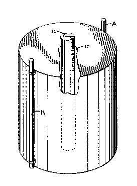
Figure 1 is a perspective view of a power cell in
accordAnce with the present invention, partly broken open,
usir1g a spent fuel rod from a nuclear reactor as the energy
~ol1re;
~ '~qu~`e 2 i5 a top plan vlew of the power cell a1-1d ~uel
t o-l sho~11 in Figure 1 Arld
l;laure 3 ls an enlarged cross section thsough the
1~ Inlle~;mo~t tu~ of the ~ul~i-ley~r- film in ~h~ power cell,
indicated by the ~ection li~ 3-~3 in ~'lgu~e ~, and
showing the bleeder regulator and the anode and cathode on
tt1e outside of the power cell.
~efore explaining the disclosed embodiment of the
present invention ln detail it is to be understood that the
invention is not limited in its application to the details
of the particular arrangement shown since the invention is
capable of other embodiments. Also, the terminology used
herein is for the purpose of description and not of limita-
tion.DETAILED DESCRIPTION
~ eferring flrst to Figures l and 2, in broad outline
the present power cell is a generally cylindrical structure
having a central longltudinal ope~ing 1~ whlch rëceive5 a
high frequency electromagnQtic radlation source in the form
of a spent fuel rod ll ~rom a nuclear reactor. The power
cell is composed of a spiral-wound multi-layer film having
a thickness of about l mm., for example. In one practical
emodiment, the power cell has an outside diameter of 24
cm., an inslde diameter of 4 cm., and a height of 30.5 cm.,
and it has lOO or so turns of a spiral-~ound multi-layer
film having its successive turns in contiguous relation-
ship.
Referring to Figure 3, the innermost turn of the
multi-layer film of the power cell has, from the inside
out: an emitter layer E in the form of an aluminum film
which is 127 microns thick, a first intermediate layer 12
2~2~279
o~ glass whlch is 51 microns thick, an aluminum film col-
lector layer c which is 127 microns thick, and on the side
t:oward layer 12 has a much thinner coatin~ C' of a ma-terial
that emits Compton electrons, coating C' being a second
5 intermediate layer of the film, a third intermediate layer
13 of glass which is 254 microns thick, an aluminum film
retarding layer R which is 127 microns thick, and a glass
outer insulation layer 14 which is 254 microns thick.
~'~eferably, the Compton effect layer C' has a thickness of
S()-10~ Angstroms. ~'he emltter l~yer E' in the next turr1 of
the f llm ~u-tward ln the ~ell ls st~own lr~ phantom in ~ligurë
~ engaging the outer face o~ the ou~er insulatlon layer 14
of t1~e lnnermost turn.
In each turn of the fllm, the emitter layer E is a
~'irs-t electrlcally conductive layer, the collector layer C
is a second electrlcally conductive layer, the retarding
layer R is a thlrd electrically conductive layer, the first
and third intermedlate layers 12 and 13 have a substantial
insulating effect, the second intermediate layer C' has a
substantial Compton effect, and the outer layer 14 insul-
ates the retardlng layer R from the emitter layer in the
next turn outward.' Preferably, layers l2, l3 and l4 are of
the same dielectric materl-al, cUch as glass. The emitter
Layer in each turn of the film ls connected conductively to
~n external nnode A, Which is gro~nded. ~ha colle~or
layer C in each t~rn o~ the film is connec~ed to an exter-
nal cathode K. The electrical load that is to be energized
hy this power cell is connected across the anode A and
cathode K.
If desired, the emitter layer E, the collector layer C
or the retarding layer R, or any two of them or all three
may have a thin coating or coatings, like the coatlng C'
shown on collector layer C, of a different material, such
as selenium, lead, copper or silver, etc. to modify the
emission, collection or retarding performance of that
layer.
l'he optimum thickness of each electrically conductive
layer E, C and R depends upon the radiation source. 'I'he
2~2~2~
intensity of the electromagnetic radiation of a ~iven w~ve-
leng-th decreases exponentially as it passes through an
absorber like each of these layers. Therefore, the thick-
ness of each of these layers is selected to match the
radiation characteristics of the source 11. This is also
true of the one or more Compton effect layers like t~le
Layer C' in the cell.
lnsteAd of glass, each insulation l~yer 12, 1~ alld 14
may be of "Lucite" or other ~ult~ble pl~sti~ or ceramic, o~
i~ m~y b~ of certaln metals, dependlng ~pon the temperatu~e
at WtliCh the power cell operates.
~ e essential requirement of coating C' i5 that it
rele~se a relatively large number of secondary Compton
electrons as a result of the photoelectrons passing through
it.
l'he retarding layer R will be at a relatively high
negative voltage, such as -3000 volts, depending upon the
thickness of the first and second intermediate layers 12
alld 13. 'rhe grea-ter the thickness of the insulatlon layer
between two successlve conducting layers, the greater will
be the voltage difference between them in response to a
particular electromagnetic radiation. The collector layer
ls kept at about -440 voltç through a bleeder regulator 15
~ig. 3) connected betwèen it and ~he retarding l~yer R.
The regulator 15 has an operatlonal amplifier 16 with
its positive input terminal connected through a resistor 17
to the retarding layer R of each turn of the film and
through a resistor 18 to the collector layer C of each turn
of the film. Resistors 17 and 18 constitute a voltage
divider for applying to the positive input terminal of
amplifier 16 an input voltage that is proportional to the
voltage difference between layers R and C. The negative
input terminal of amplifier 16 is connected through a
resistor 19 to the retarding layer R and through a Zener
diode 20 to the collector layer C. A feedback resistor 21
is connected between the negative input terminal and the
output terminal of amplifier 1~. A shunt transistor 22 has
292~279
, .
its base electrode 23 connec~ed to ttle output terminal of
ampllf~ier 16 its collector electrode 24 connected to the
~eta~ding layer R and ~ts emitter electrode connected
througtl a resistor 26 to the collector layer c.
In the operation of the bleeder regulator the Zener
diode 20 provides a fixed reference potential on the nega-
tLv~ ir.put te~minal of oper~tional amplifier 1~ whilc the
voltc~ge divider 17, 18 provldes on the positive inF-ut
~er~ l of ampll~ler 16 a voltag~ wl)ic~ is Proport1Orl~l. to
1~ t~ voltage diffQren~e b~tw~e~ ~ëtardln~ l~y~r ~ ~d col-
le~tor layer C. ~he operational ampli~ler produces an
error slgnal on lts outp~t terminal that controls the rate
of current discharge from retarding layer R through shunt
transistor 22 and resistor 2fi to the collector layer C.
lS In the operatlon of thls power cell, the emitter layer
E in the turn of the fllm closest to the source 11 of high
fre~uency electromagnetlc radlatlon acts as an absorber ln
which some of the radlatlon photons cease to exlst and
photoelectrons are emltted generally ln the same direction
as the electromagnetlc radiatlon, l.e., toward the collec-
to~ layer C in this turn of the fllm. To some extent in
the insulatlon layer 12 next to the first emltter layer E
and to a much greater extent in the second intermcdlate
layer C', photoel~ctrons ~rom layer E undergo lonizing
colllslons and release lower energy secondary Compton elec-
trons which move generally ln the same directlon as thephotoelectrons (and the electromagnetlc radiation). The
adjoinlng collector layer C recelves the negatlve charges
of the photoelectrons from emltter layer E and the lower
energy secondary Compton electrons. Collector layer C also
acts as an absorber of ~ome of the hlgh frequencY electro-
magnetic radiation from source 11 which reaches it without
having been absorbed by the first emitter layer E. As a
radiation absorber collector C emits photoelectrons which
move through the lnsulatlng layer 13 to the retarding layer
E~ and in doing so cause lower energy secondary Compton
electrons to be released which also move to the retarding
layer. 1`he primary function of the outer insulating layer
2~2~2~9
1q is to insulate tt,e retarding layer R ~n that turn of ttle
film from the emitter layer E in the nex-t turn.
Essentially, the same process takes place in eactl suc-
cessi~e turn of the multi-layer film outward from the turn
F-l2-G-C-l3-~-l4 clssest to the radiation source ll. Only
a very small percentage of the photons of electromagnetic
rnd1atlon energy is absorbed ln eactl turn of the multi-
layct film, so that it takes a la~ge number of these turrls
to absorb substa~ti~lly ~ll of thls ener~y ~rom the source
'1~ 11.
It i5 to be understood that this invention may tlave a
structural form different from the spiral-wound film that
forms a cylinder ln the disclosed embodiment. The composi-
tion and thlckness of each electrlcally conductive layer
and each intermediate layer in the cell may differ from the
specific example given, so long as each layer is capable of
performing its intended functlon. If desired, the retard-
ing layer R may be omitted, leaving the fllm as a five-
l~yer body made up of electrically conductive emitter and
collector layers, a flrst intermediate insulating layer 12
nnd a second intermediate layer C' of a material with a
substantial Compton effect sandwiched between them, and an
insulatior1 layer on the other slde o~ the collector layer.
~lowever, ln a~y such modlfled embodlment lt ls crucially
i~llportant that each insulation layer ~e.g., 12 and 13)
between an radiation-absorbing layer and a charge-collect-
lng layer be within the 50 Angstroms - 500 microns range of
thickness so that a relatlvely large number of secondary
Compton electrons will have enough kinetic energy to reach
the charge-collecting layer, so their charges are added to
the charges of the photoelectrons released from the radia-
tion-absorbing layer, as described.
~.~