Note: Descriptions are shown in the official language in which they were submitted.
~` 2~2~4S
The present invention generally relates to an auto-
tuning circuit for an active filter used in i~video sig-
nal processing. More particularly, it relates to a
circuit for automatically tuning an active filter used
in a color television (TV) receiver, such as a delay
line for delaying video signals or a band-pass filter
for limiting the band of chrominance signals.
In recent years, the active filtering technology
and the semiconductor manufacturing technology have
advanced, making it possible to incorporate active fil-
ters of video band (0 - 10 Hz) into an integrated cir-
cuit (IC). To incorporate active filters of this type
into an IC had been regarded as u~..k~t-difficult.
The resistance, capacitance, etc. of a filter of
this type incorporated in an IC, which determine the
transfer characteristic thereof, differ about 20% from
the design values due to the inadequate control of the
IC manufacturing process. Hence, it is necessary to
adjust the resistance, capacitance, etc. of the filter
built in the IC, e.g., a delay line for delaying Y
(luminance) signals or a band-pass filter for filtering
chrominance signals.
Additional IC manufacturing steps must be performed
to adjust the resistance, capacitance, etc. of the
filter incorporated in each IC. Further, these electri-
cal properties of the filter cannot always be adjusted
with sufficient accuracy, and may change due to
2û2~4~
-- 2
temperature drift. In view of this, it is not necessar-
ily advisable to adjust the resistance, capacitance,
etc. of the filter.
Hence, various auto-tuning circuits have been
invented which automatically adjust the resistance,
capacitance, etc. of a filter built in an IC.
Fig. 6 illustrates one of these circuits, which is
a phase-locked loop (PLL) including a conventional
voltage-controlled filter.
In this auto-tuning circuit, a reference clock sig-
nal A is supplied from an input terminal 1 to a phase
detector 2 and a voltage-controlled filter 3. The phase
detector 2 compares the phase of the clock signal A with
that of the signal B output by the filter 3, and gener-
ates a voltage corresponding to the phase difference
between the signals A and B. This voltage is applied
via a loop filter 4 and a DC amplifier 5 to the voltage-
controlled filter 3. The voltage adjusts the transfer
characteristic of the filter 3 such that the filter 3
can process an input video signal into a video signal
having desired characteristics.
Fig. 7 illustrates the phase detector 2 and the
loop filter 4 in detail. The detector 2 comprises a
current source Io, a double-balanced differential
amplifier comprised of transistors Q01 to Q06, and a
current mirror comprised of transistors Q07 and Q08.
The reference clock signal A is supplied between the
~S345
common base of the transistors Q03 and A06 and the com-
mon base of the transistors Q04 and Q05. The signal B
output by the voltage-controlled filter 3 is supplied
between the bases of the transistors Q01 and Q02. An
output Ix, which corresponds to the phase difference
between the signals A and B, is supplied from the col-
lectors of the transistors Q04 and Q06. The output Ix
is supplied to the DC amplifier 5 through a capacitor Cx
which constitutes the loop filter 4.
The voltage-controlled filter 3 is a delay line or
a low-pass filter having such a second-order transfer
characteristic, either shifting the phase of the refer-
ence clock signal A by 90.
The operation of the circuit shown in Figs. 6 and 7
will now be briefly explained, with reference to the
timing chart of Fig. 8.
The first signal A input to the phase detector 2
has the waveform A shown in Fig. 8, and the second sig-
nal B input to the detector 2 has the waveform B shown
in Fig. 8. The second signal B has been generated by
passing the first signal A through the voltage-
controlled filter 3, thereby phase-shifting the signal A
or delaying the same by 135. Both the first signal A
and the second signal B have a sufficient amplitude.
The phase detector 2 outputs a current Ix which repre-
sents the phase difference between the signals A and B
and has the waveform specifically shown at C in Fig. 8.
202~3~5
This current Ix is accumulated in and discharged from
the capacitor Cx forming the loop filter 4.
As is evident from C in Fig. 8, the electrical
charge supplied out of the capacitor Cx is greater than
the charged accumulated therein. Hence, the output
voltage of the loop filter 4 decreases with time. The
output voltage of the loop filter 4 is amplified by the
DC amplifier 5 and is then applied to the voltage-
controlled filter 3. The filter 3 is designed to shift
the phase of the first signal A by an amount propor-
tional to the input voltage. Therefore, the PLL is sta-
bilized when the charge supplied from the capacitor Cx
is equal to that accumulated therein, that is, when the
signal B is out of phase from the signal A by 90.
More precisely, the reference clock signal A is a
3.58 MHz signal output by an oscillator (not shown)
which is used to demodulate a chrominance signal, and
the voltage-controlled filter 3 is a delay line. The
transfer characteristic of this delay line is adjusted
automatically such that the delay line shifts the phase
of the signal A by 90 at the frequency of 3.58 MHz.
In other words, the delay line outputs a video signal
delayed by about 70 nsec with respect to the input video
signal (i.e., a luminance signal).
As is shown in Fig. 6, the control voltage applied
to the filter 3 is also applied to the other filters
formed in the same IC, whereby these filters are
2~26345
-- 5 --
automatically adjusted to have desired transfer
characteristics. This is because the resistors and
capacitors incorporated in the IC have characteristics
different slightly from the design values by only +l to
3%. However, this auto-tuning circuit (Fig. 6) has a
drawback which will be discussed below.
Fig. 9 illustrates a conventional delay line cir-
cuit which is used as a Biquad-type voltage-controlled
filter and which is similar to the type disclosed in
U.S. Patent 4,748,422. As is shown in Fig. 9, this
delay line circuit has transistors Q1 to Q31, resistors
Rl to R14, capacitors Cl and C2, a voltage source vcc,
and a bias source Vl. An input signal A is supplied to
the base of the transistor Ql, and an output signal B is
supplied from the emitter of the transistor Q16. A con-
trol voltage Vx is applied to the bases of the transis-
tors Q3, Qll, and Q17. A reference voltage Vref is
applied to the bases of the transistors Q4, Q12, and Q18.
Let us determine the transfer function of the fil-
ter shown in Fig. 9. Assuming that the resistor Rl has
a resistance twice as much as the resistance y of the
resistor R2, we obtain:
S2 ; 2C2y S t 2ClC2y2
2C2y 2ClC2y2
where a is the transfer coefficient of the control
transistors Q3 and Q4 and also that of the control
2 ~ 2 5 ~ 4 ~
-
-- 6
transistors Qll and Q12, and is less than 1 (a < 1).
Obviously, this filter (Fig. 9) has a stable ampli-
tude characteristic and can function as a delay line.
It should be noted that the transfer function a, common
to the transistors Q3, Q4, Qll, and Q12, iS Iout/Iin as
is illustrated in Fig. 10 illustrating a delay line.
Also it is apparent that the transfer coefficient a can
be adjusted by changing the control voltage Vx, whereby
the transfer function (i.e., the delay time) of the
delay line is changed.
Let us now discuss the influence of the crosstalk
component of the signal leaked through the control volt-
age line connected to the voltage-controlled filter 3,
with reference to Fig. 11 which shows a circuit for con-
trolling the transfer function of the filter illustratedin Fig. 9. The circuit shown in Fig. 11 has two lines
connected to the control voltage source Vx and the ref-
erence voltage source Vref and having output impedances
Rr and Rx. It further comprises transistors QA and QB
whose bases are connected to the lines, respectively,
and a current source Ic for these transistors QA and QB.
When the current from the current source IC contains
an AC component resulting from the input signal A, the
emitter currents of the transistors component QA and QB
connected to the voltage sources Vx and Vref change,
thereby changing the base currents IB f both transis-
tors QA and QB. Consequently, the current IB and the
2~2~34~
impedances Rr and Rx cause a voltage drop, and the AC
component is inevitably supplied through the control
voltage lines.
Further, a signal component is supplied to the col-
lector of the transistor QB. As a result of this, ahigh-band component~ leaks into the bias line for
applying the reference voltage Vref, due to the base-
collector parasitic capacitance CCB of the transistor
QB. Hence, the reference clock signal for adjusting the
transfer function of the delay line is a 3.58 MHz signal
for demodulating chrominance signals, the 3.58 MHz
component will leak into the delay lines for processing
luminance signals. This 3.58 MHz component will result
in slant stripes appearing on the CRT screen of a TV
receiver, and should therefore be removed. The para-
sitic capacitance CCB will affect the other bias lines
in the same manner.
The loop filter 4 is connected between the phase
detector 2 and the AC amplifier 5. The transfer charac-
teristic of this filter 4 can be altered by externalmeans. Therefore, in most cases, the capacitor Cx is
provided outside the IC and connected to the IC. More
precisely, as is shown in Fig. 12, the capacitor Cx is
connected by a terminal pin P to aluminum wire connect-
ing the phase detector 2 and the DC amplifier 5. Animpedance Rz is provided between the terminal pin P and
the aluminum wire, because of the other aluminum wires
2 0 ~ 4 ~
formed in the IC, t~the bonding wires connecting the IC
and the chip frame~ and the chip frame. Hence, while
the phase detector 2 is comparing the signals A and B,
the clock component at the input of the DC amplifier is
twice as much (2 fsc) and leaks to the delay line. This
clock component will result in slant stripes appearing
on the CRT screen of the TV receiver, too.
As has been mentioned, in the conventional circuit
shown in Fig. ll, both the reference clock component and
lo the clock component twice as much as the reference clock
component leak to the filters processing the video
signals. As a consequence, slant stripes appear on the
CRT screen of the TV receiver.
When the conventional auto-tuning circuit lO is
connected to a band-pass filter (BPF) 6 for processing
chrominance signals as is shown in Fig. 13, and a
3.58 MHz signal is used as a reference clock signal, the
3.58 MHz clock signal leaks all the time the circuit lO
is operating. The band-pass filter 6, which is an
active filter, inevitably generates a crosstalk signal
CW. The crosstalk signal CW is supplied to a color sig-
nal demodulating circuit ( DEMO) 8 through an automatic
color control circuit (ACC) 7. Hence, the DEMO 8 demod-
ulates the signal CW, adversely influencing a color-
difference signal DC and ultimately impairing the whitebalance on the CRT screen. Further, the crosstalk sig-
nal Cw is supplied from the ACC 7 also to a color killer
2~26~4~
g
circuit 9, along with a burst signal, inevitably causing
the color killer circuit 9 to make errors.
The above description is limited to the case where
the conventional auto-tuning circuit is used to control
a voltage-controlled filter. Nevertheless, the conven-
tional auto-tuning circuit can be used to control a
current-controlled filter, in which case, too, the cir-
cuit will make the same problems as mentioned above.
It is, therefore, an object of the present inven-
tion to provide a new and improved auto-tuning circuit
for an active filter used in ~video signal processing,
which can automatically adjust the active filter with
high efficiency, without forming slant stripes on a CRT
screen or impairing white balance on the CRT screen.
According to one aspect of the present invention,
there is provided an auto-tuning circuit for an active
filter used in video signal processing, said circuit
comprising:
a voltage-controlled filter used as~active filter
for imparting a predetermined transfer characteristic to
a signal having a component related to a television
signal, said transfer characteristic being adjustable in
accordance with a voltage;
PLL means connected to the voltage-controlled
filter, for applying to the voltage-controlled filter a
control voltage corresponding to the phase difference
between a reference signal and an output signal obtained
Z02~3~5
- 10 --
by passing the reference signal through the voltage-
controlled filter; and
switching means for allowing transfer of signals
between the voltage-controlled filter and the PLL means
r ~ 5 ~ at least one of the horizontal blanking periodsa~d_
vertical blanking periodsof the television signal.
According to another aspect of this invention,
there is provided an auto-tuning circuit for a plurality
of active filters used in video signal processing, said
circuit comprising:
a plurality of voltage-controlled filters used as
active filters for imparting a plurality of predeter-
mined transfer characteristics to signals having a com-
ponent related to a television signal, said transfer
characteristics being adjustable in accordance with a
voltage;
PLL means connected to at least one of the plural-
ity of voltage-controlled filters, for applying to all
of the plurality of voltage-controlled filters a control
voltage corresponding to the phase difference between
a reference signal and an output signal obtained by
passing the reference signal through ~K~at least one
voltage-controlled filter; and
switching means for allowing transfer of signals
between the PLL means and the at least one voltage-
controlled filter for at least one of the horizontal
blanking periodsand vertical blanking periodsof the
2~263~1~
television signal.
According to still another aspect of the present
invention, there is provided a filter auto-tuning cir-
cuit comprising:
an active filter whose transfer function can be
changed in accordance with a control voltage or a con-
trol current;
a phase detecting circuit for detecting the phase
of a first reference signal and that of a second refer-
ence signal and outputting a signal representing the
phase difference between the first and second reference
signals;
first means for supplying a signal output by a ref-
erence signal source to the phase detecting circuit
through a first signal path, as first reference signal;
second means for supplying the signal output by the
reference signal source to the phase detecting circuit
through a second signal path, as second reference
signal;
a loop filter for smoothing the signal output by
the phase detecting circuit;
a direct-current amplifier for supplying the active
filter with a voltage or current for controlling the
transfer function of the active filter, said voltage or
current being generated from the voltage output by said
loop filter; and
third means for operating the phase detecting
~(12~:3~5
~ iug o~
circuit~the horizontal blanking period ~d~vertical
blanking period of a television signal.
In the present invention, when the active filter,
which is controlled by either a voltage or a current, is
used in processing Y signals, a reference clock signal
has a duration equal to the blanking period of the tele-
vision signal, and the phase detecting circuit is oper-
ated during the blanking period of the television
signal. Hence, a leakage component, if output from the
auto-tuning circuit, will not adversely influence the
quality of the image displayed on a CRT screen. On the
other hand, when the active filter is used in processing
chrominance signals, the phase comparing circuit is
operated during the blanking period of the television
signal, excluding the burst period. This is because a
leakage component, if output from the auto-tuning
circuit, may adversely influence the burst signal to
cause color drift or the like. Hence, a leakage
component, if any, will not adversely influence the
quality of the image displayed on a CRT screen.
This invention can be more fully understood from
the following detailed description when taken in con-
junction with the accompanying drawings, in which:
Fig. 1 is a block diagram showing an auto-tuning
circuit for an active filter, which is a first embodi-
ment of the present invention;
Fig. 2A is a circuit diagram showing a switching
;- 2(~2-~34~S:
- 13 -
circuit incorporated in the auto-tuning circuit shown in
Fig. l;
Fig. 2s is a circuit diagram showing a switching
circuit of another type, which can be incorporated in
the auto-tuning circuit shown in Fig. l;
Figs. 2C, 2D, 2E and 2F are circuit diagrams illus-
trating various circuits for generating switching
pulses;
Fig. 3 is a timing chart representing the time
relationship among the signals used and generated in the
circuit illustrated in Fig. 2F;
Fig. 4 is a block diagram showing an auto-tuning
circuit for an active filter, which is a second embodi-
ment of the present invention;
Fig. 5 is a block diagram illustrating an auto-
tuning circuit for an active filter, which is a third
embodiment of the present invention;
Fig. 6 is a block diagram showing a conventional
auto-tuning circuit for an active filter;
Fig. 7 is a circuit diagram showing the phase com-
paring circuit incorporated in the circuit illustrated
in Fig. 6;
Fig. 8 is a timing chart explaining the operation
of the phase comparing circuit illustrated in Fig. 7;
Fig. 9 is a circuit diagram illustrating a voltage-
controlled filter;
Fig. lO is a diagram showing the circuit for
- 2~34~
- 14 -
controlling the transfer function of the filter shown in
Fig. 9;
Fig. 11 is an equivalent circuit diagram of the
circuit shown in Fig. 10;
Fig. 12 is an equivalent circuit diagram of a loop
filter formed in an IC; and
Fig. 13 is a block diagram illustrating a circuit
for processing chrominance signals, wherein the
conventional auto-tuning circuit is used to control
a band-pass filter (BPF) for processing the chrominance
signals, and explaining how a leakage of the reference
clock signal adversely influences the quality of the
image on a CRT screen.
Reference will now be made in detail to the pres-
ently preferred embodiments of the invention as illus-
trated in the accompanying drawings, in which like
reference characters designate like or corresponding
parts throughout the several drawings.
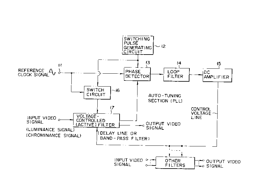
Fig. 1 is a block diagram showing an auto-tuning
circuit for an active filter, which is the first embodi-
ment of the present invention.
A reference clock signal is supplied to an input
terminal 11, and further to a phase detector 13 and a
switch circuit 16. A switching pulse generating circuit
12 supplies switching pulses to the phase detector 13.
For a period of time corresponding to the width of each
pulse, the phase detector 13 compares the phase of the
2~2~34~
reference clock signal with that of a signal output by a
voltage-controlled filter 17. Also, for this period of
time, the switch circuit 16 supplies the reference clock
signal to the voltage-controlled filter 17.
The voltage-controlled filter 17 is an active fil-
ter whose transfer characteristic changes in accordance
with the control voltage applied from an DC amplifier
15. The filter 17 has a second-order transfer function,
and is a delay line as in the conventional circuit
illustrated in Fig. 6. Alternatively, it can be a low-
pass filter.
In the embodiment shown in Fig. 1, the voltage-
controlled filter 17, which is a delay line, is used in
processing Y (luminance) signals in a color television
(TV) receiver. The switching pulse generating circuit
12 is therefore of the same type that generates horizon-
r tal blanking pulses from the fly back pulses supplied
from a flyback transformer (FBT) 12~ which is, as is
shown in Fig. 2C, driven by a horizontal deflection cir-
cuit 121 and a horizontal drive circuit 122. The refer-
ence clock signal supplied to the input terminal 11 is
the stable oscillation signal which is generated in the
color TV receiver and has a frequency of 3.58 MHz. As
has been described, the 3.58 MHz clock signal is sup-
plied from the input terminal 11 to the phase detector
13 and the switch circuit 16.
The phase detector 13 will be described in detail,
~02634~
- 16 -
with reference to Fig. 2A. As shown in this figure, the
phase detector 13 comprises a double-balance differen-
tial amplifier comprised of transistors Q41 to Q46, a
current mirror comprised of transistors Q47 to Q49, a
current-source transistor Q50, resistors R21 to R23, and
two bias sources Vll and V12. Further, the phase detec-
tor 13 has a reference clock input terminal 31, a
switching pulse terminal 32, an input terminal 33, and
an output terminal 34. The terminal 31 receives the
reference clock signal from the input terminal 11. The
terminal 32 receives the switching pulses from the pulse
generating circuit 12. The terminal 33 receives the
signal output by the voltage-controlled filter 17. The
terminal 34 supplies a signal representing the phase
difference between the Y signal and the output signal of
the DC amplifier 15.
The phase detector 13 operates in the same way as
the phase detector 2 (Fig. 7) used in the conventional
auto-tuning circuit shown in Fig. 6, except for the fol-
lowing point. While the switching pulse signal supplied
to the input terminal 32 remains at a high level, the
transistor Q50 is on, whereby a current is supplied to
the phase detector 13, and the detector 13 therefore
compares the phase of the reference clock signal and
that of the signal output by the filter 17. Conversely,
while the switching pulse signal supplied to the termi-
nal 32 remains at a low level, the transistor Q50 is
~ ~26345
- 17 -
off, whereby no currents are supplied to the phase
detector 13, and the detector 13 cannot compare the
phase of the reference clock signal and that of the sig-
nal output by the filter 17.
The switch circuit 16 will be described in detail,
with reference to Fig. 2B. As is illustrated in this
figure, the switch circuit 16 comprises a differential
amplifier comprised of transistor Q51 to Q56, a current
mirror comprised of Q57 and Q58, an output transistor
Q59, current sources Ill to I13, a reference voltage
source V13, a bias source V14, and two resistors R24 and
25. The switch circuit also ~ an input terminal for
receiving the reference clock signal, an input terminal
for receiving the switching pulses, and an output termi-
nal 43 for outputting a signal. While the switching
pulse signal supplied to the input terminal 42 is at the
high level, the terminal 43 outputs a reference clock
signal at the high level. While the switching pulse
signal is at the low level, the terminal 43 outputs the
reference voltage applied from the reference voltage
source V13.
The loop filter 14, the DC amplifier 15, and the
voltage-controlled filter 17, which constitute the auto-
tuning circuit (Fig. 1), along with the pulse generating
circuit 12, the phase detector 13, and the switch cir-
cuit 16, are identical to their counterparts 3, 4, and 5
of the conventional auto-tuning circuit illustrated in
~025~4~
- 18 -
Fig. 6. Further, the voltage-controlled filters other
than the filter 17, which are formed in the same IC, are
of the same type as those incorporated in the conven-
tional auto-tuning circuit (Fig. 1).
In operation, while the switching pulse signal is
at the high level, that is, during the horizontal bla-
nking period, the reference clock signal (i.e., the
3.58 MHz signal) is input to the voltage-controlled
filter 17, and the phase detector 13 performs its
function. On the other hand, while the switching pulse
signal is at the low level, that is, during the period
other than the horizontal blanking period, the 3.58 MHz
signal is not input to the filter 17, and the phase
detector 13 is stopped. Hence, it is during the hori-
zontal blanking period that a 3.58 MHz signal component
may leak into the control voltage line connected to the
DC amplifier 15 or the bias line common to the other
filters. Should a 3.58 MHz signal component leak~ ~o,
during the horizontal blanking period, it would not
impair the quality of the image displayed on the CRT
screen of the TV receiver.
Fig. 4 is a block diagram showing an auto-tuning
circuit for an active filter, which is the second embod-
iment of the present invention. This auto-tuning cir-
cuit is identical to the circuit shown in Fig. 1, except
for three points. First, it has no components equiva-
lent to the switch circuit 16. Second, a circuit 18 for
~ - 19- 2~6345
attenuating the reference clock signal is connected to the
input of a voltage-controlled filter 17. Third, an amplifier
circuit 19 is connected to the output of the voltage-
controlled filter 17.
In the second embodiment, the smaller the amplitude of
the reference clock signal supplied to the filter 17, the
smaller the signal component leaking to the other filters
formed in the same IC will be. Thus, there will be no
problems as far as the quality of the image on the CRT screen
is concerned, if the amplitude of the reference clock signal
is reduced so much that the signal component leaking to the
other filters is too small to be detected. However, when the
clock signal having so small an amplitude is supplied from
the filter 17 to a phase detector 13, the phase detector 13
may fail to perform its function well (that is, its operating
efficiency may decrease while the differential circuit used
in the detector 13 operates in a linear region). In order to
prevent such malfunction of the detector 13, the amplifier 19
is connected between the voltage-controlled filter 17 and the
phase detector 13.
Fig. 5 is a block diagram showing an auto-tuning
circuit for an active filter, which is the third embodiment
of the present invention. This circuit is a modification
of the auto-tuning circuit shown in Fig. 4, and is
characterized in two respects. First, the amplitude
of the reference clock signal supplied to
X
2~263~
- 20 -
an input terminal 11 is reduced, thus decreasing the
signal component leaking to the filters other than a
voltage-controlled filter 17 thereby to prevent deterio-
ration of image quality. Second, this clock signal is
amplified by amplifiers 20 and 19 to such a degree that
a phase detector 13 performs its function well.
The switching pulse generating circuit 12 need
not be limited to the type illustrated in Fig. 2C. One
of the other types of circuits, which are shown in
Figs. 2D, 2E, and 2F can be used in accordance with the
4~a~ in which the active filter is used.
More specifically, the switching pulse generating
circuit shown in Fig. 2D or 2E is used, like the circuit
~ in Fig. 2D, in the case where the active filter 17
built in the IC is employed to process Y signals (i.e.,
luminance signals). The circuit of Fig. 2D is designed
S~lin p~S~
to generate switching pulses by ~up4rpo3irl~ vertical
blanking pulses on horizontal blanking pulses, the ver-
tical blanking pulses being supplied from a vertical
blanking pulse generating circuit 124. The circuit of
Fig. 2E is designed to generate switching pulses from
only the vertical blanking pulses output by a vertical
blanking pulse generating circuit 124.
The switching pulse generating circuit shown in
Fig. 2F is used in the case where the active filter 17
built in the IC is employed to process C signals (i.e.,
chrominance signals) and composite video signals. The
`~ 2a2634~
- 21 -
circuit comprises a monostable multivibrator. The
monostable multivibrator is triggered by a flyback
pulse 1 of the same type supplied to the circuit 12 of
Fig. 2C, and generates a switching pulse~ 2 which is, as
is shown in Fig. 3, at the high level during the hori-
zontal blanking period but not during the ch~roma-burst
period.
As may be understood from the above, the switching
pulse generating circuit 12 supplies a reference clock
pulse via the switch circuit 16 to the active filter 17
and also directly to the phase detector 13, said pulse
being at the high level during the horizontal blanking
period, the vertical blanking period, or a selected part
thereof. Hence, the active filter 17 can be automati-
cally adjusted such that leakage components, if any,will not impair the quality of the image displayed on a
CRT screen.
As has been described, the auto-tuning circuit
according to the present invention can automatically
adjust an active filter used in processing video
signals, without forming slant stripes on a CRT screen
or impairing white balance on the CRT screen.