Note: Descriptions are shown in the official language in which they were submitted.
2 ~2~ ~ ~3
-- 1 --
The present invention relates to an image data pro-
cessing apparatus for converting an optical image taken
- by a camera into digital image data, and recording and
reproducing on a recording medium, and more particularly
to the one easy to extend the system and easy to achieve
the multiple functions so as to sufficiently satisfy
wide requlrements of users.
As known well, in an ordinary camera, the taken
optical image ls focused on a silver salt film, and
therefore the taken image cannot be observed unless the
fllm ls developed by chemical processing.
Recently, by contrast, an electrophotographic
system is developed and spread widely on market, which
does not requlre bothersome chemlcal processing because
the taken optical image is converted into an electrlcal
lmage data, and the image accordlng to this image data
ls dlsplayed by a televlsion receiver.
As an example of such electrophotographic system, a
still plcture recording and reproducing system is known.
In thls still plcture recording and reproducing system,
tape, disc and drum composed of magnetic material are
lnstalled in a camera main body as recording medium in a
form of cassette or cartridge, and image data is
recorded. Afterwards, the recording medium is taken out
of the camera body, and installed in a reproducing unit,
and the still picture is displayed in a television
receiver connected to the reproducing unit.
~ a ~
-- 2
In the still picture recording and reproducing
system of this sort, for example, by using a memory card
incorporating a semiconductor memory as the recording
medium, it is attempted to record at higher density and
reduce the weight and size, but actually it is in the
process of development at the present, and there are
many points to be improved.
That is, the image data processing apparatus for
converting an optical image taken by a camera into digi-
tal image data, and recording and reproducing on arecording medium is not a technically completed system
yet, and therefore it ls keenly demanded to promote the
multiple-purpose advantages more effectively, by making
the system easy to extend and easy to achieve in the
multiple functions so as to sufficiently satisfy the
versatile requests of users.
The lnventlon is devised in the light of the above
background, and lts prlmary ob~ect is hence to present
an image data processing apparatus of an extreme
excellent so as to sufficiently cope with wide requests
of users, making it easy to extend the system and easy
to achieve in the multiple functions, thereby effec-
tively promoting the multi-purpose principle.
According to one aspect of the present invention,
there is provided an image data processing apparatus
comprlsing a pickup unit for converting a taken optical
image into electric data by using solid pickup element,
- 3 - 2 ~2
and a signal processing unit for processing the data
delivered from this pickup unit to record into a
memory, both being composed independently, wherein the
pickup unit ls detachable from the signal processing
unlt, and plural types of pickup unit are prepared, dif-
ferlng ln the number of solid pickup elements contained
thereln, so that a desired pickup unit is selectively
attached to the signal processing unit to take pho-
tographs. In such constitution, the user has only to
exchange the pickup unit as required, which is advan-
tageous, economically.
According to other aspect of the present invention,
there ls provided an image data processing apparatus
comprising a pickup unit for converting a taken optical
lmage electric data by using a solid pickup element, and
a signal processing unit for processing the data deli-
vered from this pickup unit and record~ng into a memory,
both being composed independently, wherein the pickup
unit is detachable from the signal processing unit, and
a finder is disposed in the pickup unit. In such
constltutlon, the construction of the optical path ln
the pickup unit is simplified, and down sizing is pro-
moted.
According to the image data processing apparatus of
the invention for converting a taken optical image into
digital image data and compressing the data to record in
a memory, there is provided means for calculating the
- 2 ~ 3
-- 4
activity of the entire screen portion of the digital
image data and automatically setting the data com-
pression rate. In such const~tution, the compression
rate is automatically determined in a range not to cause
an extremely deterlorated picture, and the recording
capacity of the memory can be effectively utilized.
In a different aspect of the invention, there is
provided an image data processing apparatus for con-
verting a taken optical image into digital image data
through a solid pickup element and compressing the data
to record in a memory comprising first means for adding
the fixed noise components contained in the digital
image data for the portion of k exposures, second means
for summing up the digital image data obtained from ~
exposures, and third means for subtracting the output
data of the flrst means from the output data of the
second means so as to obtain the multiple exposure ima-
ges for k exposures eliminating the fixed noise. In
such constltution, the sensitivity may be raised when
taking a dark place, without elongating the exposure
time, so that it is not necessary to alter the driving
method of the solid pickup element.
Furthermore, according to the image data processing
apparatus of the invention for converting a taken opti-
cal image lnto digital image data to record in a memory,comprising a continuous filming function, wherein in the
photographic state by continuous filming function, the
, . .
2~,7~ ~3
-- 5
digltal image data corresponding to the optical image of
the first exposure is stored in the memory, and the dif-
ferential portion between the digital image data
corresponding to the optical image taken after the
second exposure and the digital image data of the first
exposure stored in the memory is recorded in the memory
by first mean, and every time a specified number of
exposures is taken in the photographic state by the
first means, the digital image recorded in the memory is
updated by second means. In this construction, the
recording capacity of the memory may be saved in con-
tinuous filming mode, and deterioration of picture
quality may be prevented.
According to a further different aspect of the
image data processing apparatus of the invention, the
taken optical image is converted into digital image data,
and is recorded ln the recording medium in predetermined
units, and the collected sound is converted into digi-
tal sound data and is recorded in the recording medium
ln the predetermined units, which moreover comprises
means for converting the transmission speed of the digi-
tal sound data to a rate higher than the standard speed,
and recording on the time axis in the predetermined units
intermittently in the recording medium. In such consti-
tution, when photographed while recording sound, theimage data can be recorded among the sound data, and the
sound and image can be synchronized when reproducing.
- 2~2~3
-- 6
According to the image data processing apparatus of
the invention, still more, for converting a taken opti-
cal image into digital image data and recording in a
memory, an option area for writing by external operation
is provided in the recording area of digital image data
of the memory, and code data for automatically
controlling the photographic operation is recorded in
this option area. In such constitution, the user can
freely set the desired photographic action individually.
A different aspect to the invention relates to an
lmage data processing apparatus comprising a main body
for converting a taken optical image into digital image
data, and a memory for recording the digital image da~a
obtained from the main body, wherein a built-in strobe
ls disposed in the main body and a connection part for
extending an external strobe is provided, and control
means for controlling both of built-in strobe and exter-
nal strobe depending on the photographic condition is
installed. In such constitution, the user may freely
comblne the built-in strobe and external strobe
depending on the photographic condition.
According to another aspect of the image data pro-
cessing apparatus of the invention for converting
~a taken optical image into digital image data and
recording in a recording medium, the data generated
correspondlng to on/off state of the key switch is
recorded, together with digital image data upon every
_ 7 _ 2 ~ ~ ~ 3 ~ ~
exposure, in an recording area of digital image data of
the recording medium. In such constitution, it is very
convenient for the user to provide the taken image with
an original meaning freely.
According to a further different aspect of the
invention, there is provided an image data processing
apparatus comprlsing a main body for converting a taken
optical image into digital image data, and a card-shaped
memory for recording the digital image data obtained
from the main body, being inserted in the main body,
wherein the card-shaped memory inserting part of the
main body possesses a card-shaped connector which can be
inserted instead of the card-shaped memory, and a
recording device capable of transferring data to the
mainbody through this card-shaped connector. According
to this constitution, it is not necessary to install
other connector for connecting with the recording device
than the card-shaped memory insertion part and the
structure may be simplified.
According to a still different aspect of the inven-
tion, there is provided an image data processing appara-
tus comprlsing a camera for converting a taken optlcal
image into dlgital image data, means for wrltlng the
dlgital image data delivered from this camera into first
and second memorles, means for readlng out the other ln
the writing state of one of the first and second
memories by this writing means, and a recording device
20~ ;3~
-- 8
for recordlng the digital image data being read out by
this reading means. In this structure, as far as the
data quantity is not excessive, it is not necessary to
define the camera side data output if the recording
speed of the recording device is slow when transferring
to the recording device, and the data transfer of high
efficiency is realized.
Another image data processing means of the inven-
tion for converting a taken optical image into digital
image data and recording in a card-shaped memory compri-
ses a mountlng part for mounting a card-shaped memory,
plural connectlng parts for connecting plural external
devlces, and an editlng machine havlng data processing
means for compresslng and expandlng the dlgital image
data supplied from the card-shaped memory and external
devices connected to the mounting part and plural con-
necting parts. In such constitution, the digital image
data supplied from the card-shaped memory and external
devices are directly compressed and expanded, and
supplied into the card-shaped memory and external devi-
ces, so that the image data processing may be done effi-
clently.
The invention also relates to an image digital
processing apparatus for reproducing the digital image
data obtained by taking with a digital still camera and
displaying on a screen, which comprises a recording
medlum in which plural dlgital image data are recorded,
2 ~ 3
g
retrieval means for retrieving desired digital image
data on the basis of the header information attached to
the dlgital image data recorded in the recording medium,
display means for displaying the plural digital image
data retrieved by the retrieval means by distributing
into display regions of the divided screens, an exten-
sion memory for recording the digital image data being
retrleved which cannot be fully displayed by the display
means, and control means for displaying the digital
image data recorded in this extension memory by distri-
buting into display regions of the display means by
external operation. In such constitution, the plural
retrieved images can be observed easily, which is very
convenient in retrleval of a huge quantlty of images.
The image data processing apparatus of the inven-
tlon is lntended to reproduce the digital image data
obtained by taking with a digital still camera and
display on the screen, wherein a first sub-menu is
dlsplayed wlth respect to the mode operated and spe-
clfled from the maln menu, and a second sub-menu is
displayed according to the mode operated and specified
from the first sub-menu, and the lmage data is processed
in this system, which further comprises recording means
for recording the data having programmed the operation
specification of the series of processing procedure with
respect to a specific processing procedure~ and execu-
tion means for automatically executing the specific
2~2~ ~3
-- 10 --
processing operation on the basis of the data recorded
ln this recording means. In such constitution, it is
very convenient because the user can perform specific
processings to be executed frequently by a simple opera-
tion.
According to a different aspect of the image data
processing apparatus of the invention, it is to repro-
duce the digital image data obtained by taking with a
digital still camera and display on a screen, possessing
means for editing and processing digital image data,
which further comprises recording means for recording
the lmage data displayed in the editing and processing
step, and display means for displaying the image data
recorded in this recording means by dividing into
display regions of the divided screens in the sequence
of display in the editing and processing step. In such
constitution, the step of editing and processing the
image data may be known at a glance, and editing and
processing may be revised or modified easily.
It is another aspect of the invention to present an
image data processing apparatus for reproducing the
dlgltal lmage taken obtalned by taking with a digital
stlll camera and displaying on a screen, which comprises
a recording medium in which plural digital image data
are recorded, retrieval means for retrieving the desired
lmage data on the basis of the header information
attached to the digital image data recorded in the
~2~33
recording medium by setting a key word, first display
means for displaying the plural digital image data
retrieved by the retrieval means by dividing into
display regions in divided screens, and second means for
displaying a list of key words determined by the
retrleval means. In such constitution, the list of
plural key words and plural retrieval images can be
monitored at the same time, and a desired image will be
obtained promptly.
This invention can be more fully understood from
the following detailed description when taken in con-
~unction with the accompanying drawings, in which:
Fig. 1 is a block diagram showing an entire system
construction, as one of the embodiments of the image
data processing apparatus of the invention;
Fig. 2 and Fig. 3 are perspective views showing the
appearance of an electronic still camera mounting a
single disc pickup unit, individually;
Fig. 4 and Fig. 5 are perspective views showing the
same electronic still camera divided into a single disc
pickup unit, signal processing unit, and reproduction
unlt;
Fig. 6 is a perspective vlew showing the state of
detaching the reproduction unit from the same electronic
still camera;
Fig. 7 is an exploded perspective view showlng an
internal structure of signal processing unit;
2~2~ 3
- 12 -
Fig. 8 is an exploded perspective view showing an
internal structure of reproduction unit;
Fig. 9 is a block diagram showing an internal
structure of single disc pickup unit;
Flg. 10 is a block diagram showing an internal
structure of a twin disc pickup unit;
Fig. 11 is a block diagram showing an internal
structure of a triple disc pickup unit;
Fig. 12 ls a block diagram showing other example of
an lnternal structure of a single disc pickup unit;
Fig. 13 ls a perspective view showing the
appearance of an electronic still camera mounting a twin
dlsc plckup unlt;
Flg. 14 ls a perspective view showing the
appearance of an electronic still camera mounting a
triple disc pickup unit;
Fig. 15 is a top view of an electronic still
camera;
Fig. 16 is a plan view showing the details of a
liquid crystal display part;
Fig. 17 is a block dlagram showing a signal system
of a pickup unit;
Fig. 18 is a block diagram showing a signal pro-
cessing circult of a single disc pickup unit;
Fig. 19 is a block diagram showing a signal
processing circuit of a twin disc pickup unit;
Fig. 20 is a block diagram showing a signal
2~2~ rJ a3
- 13 -
processing circuit of a triple disc pickup unit;
Fig. 21 is a block diagram showing a signal system
of a signal processing unit;
Fig. 22 is a block diagram showing details of a
process circuit;
Fig. 23 ls a block diagram showing a signal system
of a memory card;
Fig. 24 is a block diagram showing a signal system
of a reproduction unit;
Fig. 25 is a block diagram showing a different
example of a signal processing circuit of a single disc
plckup unit;
Fig. 26 is a block diagram showing other example of
a process circuit;
Fig. 27 is a block diagram showing details of a
buffer memory part;
Fig. 28 is a block diagram showing details of a
buffer memory;
Fig. 29A and Fig. 29B are block diagrams for
explaining the operation of multiple exposure mode;
Fig. 30A and Fig. 30B are block diagrams for
explalning the operation of continuous filming mode;
Fig. 31 ls a block diagram showing details of a
compression coding circuit;
Fig. 32 is a diagram for explaining the relation
between activity and image;
Fig. 33 is a block diagram showing details of
2 ~ 3
- 14 -
a decoding circuit;
Fig. 34 is a diagram for explaining a data
recording method;
Fig. 35 ls a diagram for explaining a data format
of memory card;
Fig. 36 is a diagram for explaining the packet data
area of the same data format;
Fig. 37 is a block diagram showing details of a
voice processing circuit;
Fig. 38A to Fig. 38C are diagrams for explaining
the data recording methods;
Fig. 39A, Fig. 39B, Fig. 40, Fig. 41A and Fig. 41B
are flow charts for explaining the operatlon of pho-
tography by electronic still camera;
Fig. 42A and Fig. 42B are flow charts for
explaining the operation inreproduction of electronic
stlll camera:
Fig. 43 is a flow chart for explaining the operation
of an AE function of electronic still camera;
Fig. 44 is a flow chart for explaining the opera-
tlon of an AWB function of electronic still camera;
Fig. 45A and Fig. 45B are flow charts for
explaining the operation of compression rate automatic
setting function of electronic still camera;
Fig. 46 is a flow chart for explaining the
operation of detection of intelligent data of electronic
still camera;
2~2~
- 15 -
Fig. 47 is a flow chart for explaining an example
of intelligent function of electronic still camera;
Fig. 48 is a flow chart for explaining a strobe
function of electronic still camera;
Fig. 49 is a flow chart for explaining an example
of the same strobe function;
Flg. 50 is a perspective view showing the remote
control operation part of electronic still camera;
Fig. 51 and Fig. 52 are perspective view and side
view showing the appearance of a filing device;
Fig. 53 is a block diagram showing a connecting
method of card type connector and filing device;
Flg. 54 is a block diagram showing other example of
connecting method of card type connector and filing
device;
Fig. 55 is a block diagram showing a signal system
of filing device;
Fig. 56 is a block diagram showing details of
càmera I/F part;
Fig. 57A to Fig. 57F are timing charts showing the
operation of the same camera I/F part;
Flg. 58 ls a flow chart for explaining the data
transfer from electronic still camera to filing device;
Fig. 59 is a flow chart for explaining the data
2s transfer from filing device to electronic still camera;
Flg. 60 is a side view showing other example of
filing device;
~ ~ 2 ~ 3
- 16 -
Fig. 61 is a perspective view showing an exclusive
cable used in the same filing device;
Fig. 62 is a perspective view showing the appea-
rance of an editing machine;
Fig. 63 is a perspective view showing the appea-
rance of an exclusive keyboard;
Fig. 64 is a perspective view showing a remote
control operation part;
Fig. 65 is an exploded perspective view showing
details of card tray part;
Fig. 66 is a top view of card tray;
Fig. 67 and Fig. 68 are top view and side view for
explaining the loading operation of card tray;
Fig. 69 and Fig. 70 are top view and side view for
explaining the connection state of card tray to the con-
nector;
Fig. 71 is a perspective view showing detalls of
card tray and connector;
Fig. 72 and Fig. 73 are top view and side view for
explaining the unloading operation of card tray;
Fig. 74 is a block diagram showing a signal system
of editing machine;
Fig. 75 is a block diagram showing details of CP~
part;
Fig. 76 is a block diagram showing details of
memory card data input, output part;
Fig. 77 is a block diagram showing details of
- 17 - 2~ 3
parallel data input, output part;
Fig. 78 is a block diagram showing details of
serial data input, output part;
Fig. 79 is a block diagram showing details of other
parallel data input, output part;
Fig. 80 is a block diagram showing details of audlo
appllance control part;
Fig. Bl is a block diagram showing details of image
data input, output part;
Fig. 82 is a block diagram showing details of
display part;
Fig. B3A and Fig. 83B are flow charts for
expla~n~ng the data transfer between devlces;
Fig. 84 is a timing chart showing the data transfer
in through-mode between devices;
Fig. 85 is a tlmlng chart showing the data transfer
in compression mode between devices;
Fig. 86 is a timing chart showing the data transfer
in expansion mode between devices;
Fig. 87A and Fig. 87B are flow charts for
explaining the operation of turning on the power source
of the editing machine;
Fig. 88 and Fig. 89 are drawings showing examples
of display screen in the operating state when turning on
the power source;
Fig. 90 to Fig. 93 are drawings showing examples of
display screen in the operating state of retrieval
2~2~ ~3
- 18 -
function, together with flow charts for explainlng the
operation of the retrieval function;
Fig. 94 is a flow chart for explaining the opera-
tion of processing function;
Fig. 95 is a drawing showing an example of display
screen by processing function;
Fig. 96A and Fig. 96B are flow charts for
explaining the operation of montage function;
Fig. 97 is a drawing showing an example of display
screen by montage function;
Fig. 98 is a flow chart for explaining the opera-
tion of graphic insertion function;
Fig. 99 is a drawing showing an example of display
screen by graphic insertion function;
Fig. 100 is a flow chart for explaining the opera-
tion of text insertion function;
Fig. 101 is a drawing showing an example of display
screen by text insertion function;
Fig. 102 is a flow chart for explaining the opera-
tion of level conversion function;
Fig. 103 is a drawing showing an example of display
screen by level conversion function;
Fig. 104A, Fig. 104B, Fig. 105A, Fig. 105B,
Fig. 106 to Fig. 108 are flow charts for explaining the
operation of storage function;
Fig. lO9A, Fig. lO9B, Fig. 110 and Fig. 111 are
flow charts for explaining the operation of
2~2~:3~~3
-- 19 --
communication function;
Fig. 112 is a drawing showing an example of display
screen by external connection function;
Fig. 113, Fig. 114A, Fig. 114B and Fig. 115 are
flow charts for explaining the operation of automatic
execution function; and
Fig. 116A, Fig. 116B and Fig. 117 are flow charts
for explalning the operation of extension program func-
tion.
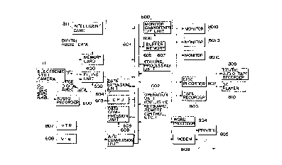
Referring now to the drawings, one of the embodi-
ments is descrlbed in detail below. Fig. 1 shows an
entire structure of the system explained in this embodi-
ment, and its outline is briefly described below. That
i9, in the drawing, numeral 11 denotes an electronic
still camera. This electronic still camera 11 converts
a taken optical lmage into a video signal by using a
solld pickup element such as CCD (charge coupled
device), and further converts this video signal into
digital image data of each form of R (red), G (green),
B (blue) and Y/C (lu~n~nce/color), and compresses the
digltal lmage data of Y/C, and delivers. This electro-
nlc still camera 11 also incorporates a microphone, and
dellvers the collected voice as the voice data in
various digital and analog forms.
Among them, the Y/C digital image data and
dlgltal voice data are recorded in a memory card 400
lncorporating a semiconductor memory, which is freely
~2~ :3~
- 20 -
detachable from the electronic still camera 11.
Besides, digital image data of R, G, B and Y/C and digi-
tal voice data are recorded in a filing device 500. The
flling device 500, in this embodiment, employs a digital
audio tape recorder as one of the reloadable recording
devlces, and possesses a recording capacity far greater
than that of the memory card 400. Between the memory
card 400 and the filing device 500, the digital image
data and digital voice data can be exchanged, and the
digital image data and digital voice data recorded in
the memory card 400 can be transferred and stored ~n the
fillng device 500.
The analog voice data collected by the electronic
still camera 11 can be recorded in an exclusive voice
recording device 800 such as audio tape recorder. The
digital image data and digital voice data recorded in
the memory card 400 and filing device 500 are read out
in the electronic still camera 11, and can be reproduced
by a small-sized liquid crystal monitor or speaker
2Q incorporated in the electronic still camera 11.
The dlgital image data and digital voice data
recorded in the memory card 400 and filing device 500
are supplied in a bus line 601 of an editing machine
600. This editing machine 600 is intended to transmit
the digital image data and digital voice data to various
peripheral devices, or process and edit the data by the
control of a CPU (central processing unit) 603 by
2~2~
- 21 -
manipulating the operation part 602 composed of the con-
nected exclusive keyboard, remote control operation part
and the like, and therefore it is made easy to extend
the system and easy to achieve multiple functions,
thereby promoting the multiple-object principle effec-
tively and satisfying wide needs of users sufficiently.
For example, the digital image data delivered from
the memory card 400 or filing device 500 is expanded in
a data expanding part 604, and the image may be selec-
tlvely displayed in externally connected plural monitors80a, 801b, 801c, ..., through buffer memory 605 and
monltor changeover I/F (interface) part 606. It is also
possible to edit or process the digital image data as
desired in an editing and processing part 607, or record
the dlgital lmage data or digital voice data in varlous
recordlng devlces, such as reloadable disc recording
dèvice 802 and tape recording device 803 connected
externally.
Using a word processor 804, furthermore, character
data may be overlaid on digital image data, or the ima-
ges may be printed out by using a printer 805. It is
moreover possible to c~_ -nicate the digital image data
and digital voice data by using a modem 806. Yet, the
digltal lmage data recorded in the frame memory of
externally connected VTR (video tape recorder) 807, or
the analog image data delivered from externally con-
nected VTR 808 once converted into digital image data by
2 ~ 2 ~ r~ ~3 3
- 22 -
A/D (analog/digital) conversion part 608 may be
compressed ln a data compression part 609, and recorded
in desired recording medium or displayed in desired
monitor.
In addltion, depending on the images displayed in
the monitors 801a, 801b, 801c, ..., the tune to be
reproduced may be changed according to the display image
by controlling an externally connected digital audio
tape recorder 809 or CD (compact disc) player 810. Or
by using an intelligent card 811 in which a program is
recorded preliminarily, the above functions may be exe-
cuted automatically in time seguence. The outline of
the system of this embodiment is described briefly
hereln, and details of parts are described below. The
parts are explalned in the following sequence.
1. Fig. 2 to Fig. 16: Explanation about the
structure of the electronic still camera 11.
2. Fig. 17 to Fig. 33: Explanation about the
signal system of electronic still camera 11.
3. Fig. 34 to Fig. 38C: Explanation about
recording format of digital image data and digital voice
data.
4. Fig. 39A to Fig. 49: Explanation about opera-
tion of various functions of electronic still camera 11.
5. Fig. 51 to Fig. 61: Explanation about
construction and operation of filing device 500.
6. Fig. 62 to Fig. 73: Explanation about
~ 0 ~ 3
construction of editing machine 600.
7. Fig. 74 to Fig. 82: Explanation about the
signal system of editing machine 600.
8. Fig. 83A to Fig. a6: Explanation about data
transfer of editing machine 600.
9. Fig. 87A to Fig. 117: Explanation about opera-
tlon of various functions of editing machine.
[structure of electronic still camera]
In the first place, the electronic still camera 11
0 i9 explained. This electronic still camera 11 compri-
ses, as shown in Fig. 2 and Fig. 3, a pickup unit 100, a
slgnal processlng unit 200, and a reproductlon unit 300.
The pickup unit 100 includes a lens 101, a built-in
strobe 102, an external strobe 103 and a finder 104,
as well as others. The slgnal processing unit 200
contains, among others, a release 201, a mode dial 202,
a liquid crystal display part 203, a power and
record/reproduction changeover switch 204, a mode set-
ting switch 204, an insertion part 206 of memory card
400, and an e~ect switch 207 for taking out the memory
card 400, as well as a built-in microphone provided in
the lower side which is not shown in the drawing. The
reproduction unit 300 comprises a small liquid crystal
monitor 301, a screen feed switch 302, a screen
ad~usting switch 303, a connector part 304 for connec-
tion to external monitor or speaker, and others, and a
built-ln speaker in the lower side which is not shown in
2 ~ 3 ~
- 24 -
the drawing.
Meanwhile, as shown in Fig. 4 and Fig. 5, the
pickup unit 100, signal processing unit 200 and repro-
duction unit 300 are designed to be separated from each
other. The pickup unit 100 and the signal processing
unit 200 are mechanically coupled together by fitting a
pair of hook parts 105, 105 ~only one is seen in Fig. 5)
disposed in the p$ckup unit 100 to a pair of receiving
parts 208, 208 disposed in the signal processing unit,
and by matching the connector part 106 disposed in the
pickup unit 100 with the connector part 209 disposed in
the signal processing unit 200, they are electrically
connected. Besides, the signal processing unit 200 and
reproduction unlt 300 are mechanically coupled together
by fittlng a palr of hook parts 305, 305 disposed in the
reproductlon unit 300 to a pair of receiving parts 210,
210 dlsposed ln the slgnal processing unit 200, and are
electrically connected by fitting the connector part 306
disposed in the reproduction unit 300 with the connector
part 211 disposed in the signal processing unit 200.
The pickup unit 100 and reproduction unit 300 are
deslgned so that the hook parts 104, 305 are detached
from the receiving parts 208, 210 so as to be released
from the signal processing unit 200, by manipulating the
release switch disposed in the lower side which is not
shown in the drawing. Accordingly, when performing pho-
tography only, as shown in Flg. 6, it is small in size,
2 ~ 2 ~
- 25 -
light in weight and convenient in carrying by detaching
the reproduction unit 300. In this case, meanwhile, the
connector part 211 is protected by fitting a protective
lid 212 on the connect or part 211 of the signal pro-
cessing unlt 200 connected with the connector part 306
of the reproduction unit 300.
Fig. 7 shows the structure of the signal processing
unit 200. In the drawing, the reference code 213a deno-
tes a main cabinet, in which a main body part 213b
approximately in a box shape enclosed by the pickup unit
100 and reproduction unit 300, and a grip part 213c to
be gripped by the right hand of the user are formed
integrally in one body. The grip part 213c contains a
battery holder 214 for accommodating batteries, a DC-DC
converter 215 for raising the battery voltage, and a
printed wiring board 216 on which the release 201, mode
dial 202, liquid crystal display part 204 and power and
recording/reproduction changeover switch 204 are
mounted.
In the main body part 213b, various circuit devices
217, 217..., and two printed wiring boards 218a, 218b
mounting the mode setting switch 204 and connector parts
209, 211 are disposed parallel and accommodated.
Between the two printed wiring boards 218a, 218b, a card
holder 219 having an e;ect switch 207 is disposed.
Thus, in the structure having the card holder 219 sand-
wlched by the two printed wiring boards 218a, 218b, the
2~2~3
- 26 -
rigidity of the card mounting portion may be enhanced
without increasing the thickness of the card holder 219,
which contributes to saving of space and reduction of
size, and also the cooling effect for the circuit devi-
ces 217 is achieved. The signal processing unit 200 is
completed as the opening of the connected side of the
reproduction unit 300 of the main cabinet 213 is closed
by the sub-cabinet 213d which is a lid.
Fig. 8 shows the structure of the reproduction unit
300. That is, 307a ls a main cabinet formed approxima-
tely ln a box shape, which accommodates various circuit
devlces 308, 308, ..., and a printed wiring board 309
mountlng small liquid crystal monitor 301, screen feed
swltch 302, scre~n adjusting switch 303, connectors 304,
306, etc. Of the main cabinet 307a, the end part of the
grip 213c side of the signal processing unit 200, that
ls, the end part at the right side in Fig. 8 is provided
wlth a slope part 307b which is sequentially lowered in
height toward the signal processing unit 200 side.
Accordingly, even in the state of coupling of the repro-
duction unit 300 in the signal processing unit 200, the
thickness of the grip part 213c is not increased as a
whole for the electronic still camera 11, so that it may
not be difficult for the user to hold. Besides, as the
opening of the coupling side of the signal processing
unit 200 of the main cabinet 307a by the sub-cabinet
307c which is a lid body, the reproduction unit 300 is
2~2~-3~3
- 27 -
completed.
Meanwhile, the sub-cabinet 307c is provided with
hook parts 305, 305. The hook parts 305, 305 are formed
in a hook shape at both ends of the hook member 305a
being approximately in a pi-shape, and the both end parts
of the hook member 304a are projected outward through a
pair of penetration holes 307ad, 307d formed in the sub-
cabinet 307c. The hook member 305a is thrust in the
leftward directlon in the drawing by a coil-shaped
spring 305b, so that the hook parts 305, 305 are stopped
at receiving parts 210, 210 of the signal processing
unit 200, and by manipulating a release switch 30cc
llnked to the hook member 305a in the rightward direc-
tion in the drawing by resisting the thrust force of the
spring 305b, stopping of the hook parts 305, 305 on the
receiving parts 210, 210 is cleared. Besides, the com-
positlon of the hook member 305a, spring 305b, and
release switch 305c applies same to the hook parts 105,
105 of the plckup unit 100.
Flg. 9 shows an internal structure of the pickup
unit 100. That is, the optical image of the subject
entering through the lens 101 is adjusted of the quan-
tity of llght by a diaphragm 107. and is led into the
finder 104 through mirrors 108, 109, and is visually
observed by the photographer. Meanwhile, the lens 101
and diaphragm 107 are integrally combined as a lens unit
110, together with motors ~not shown) for driving the
~6~3
- ~8 -
lens 101 and diaphragm 107 owing to the automatic
focusing adjustment (AF: auto-focus) function and auto-
matic diaphragm ad~ustment (AE: auto-iris) function. To
realize the AE function, the pickup unit 100 is also
provided with an AE sensor (not shown) for sensing the
quantity of light of the subject.
When the release 201 disposed in the signal pro-
cessing unit 200 is pressed, the mirror 108 ~umps up in
Fig. g by the mech~n ~ cal mechanism. As a result, the
optlcal image of the subject is once adjusted of the
quantity of light by the shutter 111, and is passed
through infrared cut filter 112 and optical low pass
filter 113, and is focused on the CCD 114. The image
signal obtalned by photoelectric conversion in the CCD
114 is sent into an image processing circuit 115 for
color separation and A/D conversion processing, and is
supplied into the signal processing unit 200. The
shutter 111 of mechanical type is used as an aid for the
electronlc shutter function by the CCD 114.
The foregoing pickup unit 100 is of so-called
single disc type having one CCD 114 inside, and,
moreover, there are prepared twin disc pickup unit
having two CCDs inslde or triple disc pickup unit having
three CCDS inslde, so as to obtain pickup images of
higher picture quality. By selectively attaching three
~ types of pickup units 100 to the same signal processing
unit 200, the entire electronic still camera 11 may be
2~2~ 3~3
- 29 -
used in three types, that is, single disc type, twin
disc type and triple disc type. By setting up such
constitution, only by replacing the pickup unit 100 only
depending on the resolution of the image to be obtained
or the quantity of data, the request of the user may be
sufficed, so that an inexpensive electronic still camera
11 may be presented on the whole.
Fig. 10 and Fig. 11 show the internal structure of
the twin disc and triple disc pickup units lOOa, lOOb,
by using the same reference codes for the same parts.
Flrst in the twin disc pickup unit lOOa, as shown in
Flg. 10, the optical image passing to rough the optical
low pass fllter 113 ls separated into RGs component and
Y component by a prism 116, and the light of each com-
ponent is individually photoelectrically converted by
two CCDs 117a, 117b. The obtained image signals of RGB
component and Y component are sent into an image pro-
cessing circult 118 for color separation processing and
A/D converslon processing, and supplied into the signal
processing unit 200.
In the triple disc pickup unit lOOb, as shown in
Flg. 11, the optical image passing through the optical
low pass fllter 113 is separated into components of R,
G, B by a prism 119, and lights of the components are
photoelectrically converted in three CCDs 120a, 120b,
120c. The obtained image signals of components R, G, B
are sent into image processing circuit 121 for A/D
2 ~ 3~3
- 30 -
conversion processing, and supplied into the signal pro-
cessing unit 200.
Between the single disc pickup unit 100 and the
twin disc and triple disc pickup units 100a, 100b, as
clear from Figs. 9, 10 and 11, the thickness of the lens
101 is different. This is because, the optical path
length from the lens 101 to the CCDs 114, 117a, 117b,
120a to 120c is longer in the twin and triple dlsc
pickup units 100a, 100b, as compared with the single
disc pickup unit 100, for the portion of the prisms 116,
ll9, and therefore it is necessary to correct the focal
length due to difference in the optical path length.
Accordingly, if it is disadvantageous in manufac-
ture or econo~y to use lens 101 of difference thlckness
between the single disc pickup unit 100 and twin disc and
triple disc pickup units 100a, 100b, the thickness of
the lens 101 used in the single disc pickup unit 100 may
be made same as the thickness of the lens 101 used in
the twin disc and triple disc pickup units 100a, 100b,
that is, the same lens 101 may be used for the single
disc pickup unit 100, and the twin disc and triple disc
pickup units 100a, 100b. In this case, as shown in
Fig. 12, an adapter 122 with a distance "~" may be
placed between the lens unit 110 and mirror loa in order
to compensate for the focal length due to differential
portion of the optical path length. Or, without using
adapter 122, the optical path length may be obtained by
237~3
- 31 -
installing an optical part such as mirror in order to
fold the optical path inside the pickup unit 100.
Meanwhile, as the lens unit 110 for the pickup units
100, lOOa, lOOb, various types such as telephoto lens
and wide angle lens can be selectively mounted.
The state of mounting the twin disc and triple disc
pickup units lOOa, lOOb on the signal processing unit
200 is shown in Fig. 13 and Fig. 14. In both pickup
units lOOa,lOOb, it is known that the thickness is
increased for the portion of the prisms 116, 119.
Besides, in the triple disc pickup unit lOOb, since the
plckup image ls of an extremely high picture quallty, a
connector part 123 (protected by a lid body not shown in
the drawing when not in use) is disposed at one side in
order to take out the digital image data of uncompressed
components R, G, B to outside, and display the image of
high picture quality on, for example, an external moni-
tor. The reason of disposing the connector part 123 for
output of R, G, B in the triple disc pickup unit loob,
instead of the signal processing unit 200, is (1) as
known from Fig. 11 in the case of tricple disc type,
uncompressed outputs of R, B, G can be obtained easily,
(2) it is a special case the request uncompressed data in
spite of massive use of data recording region, and (3)
it is disadvantageous for the space to install the con-
nector part 123 in the signal processing unit 200 which
has a narrow surface area.
2 ~ 3 3
- 32 -
Fig. 15 shows a top view of the electronic still
camera 11, particularly indicating the details of opera-
tion parts disposed in the signal processing unit 200.
That is, the release 201 is a switch to be pressed
mechanically, and by a first step operation to press
with a small pressure, it establishes a state of taking
in light necessary for AE function, AF function and
automatic color temperature adjustment (AWB: automatic
white balance) function, and by a second step operation
to press with a greater pressure, actual photography is
taken.
The mode dial 202 has part of the peripheral edge
of the dlsk exposed to outside to be rotated in
handllng, and when it is manipulated together with a
mode settlng switch 205, various conditions necessary
for photography are established. As the power and
record/reproduction changeover switch 204 is dislocated
from the "OFF" posltion, the power is turned on, and it
i9 ready to execute all actions of the electronic still
camera 11. At "REC9' position, it is the record mode and
the electronic stlll camera 11 is ready to write image
and voice data into the memory card 400 and filing
device 500, and at "PLAY" position, it is the reproduc-
tion mode and the electronic still camera 11 reproduces
the image and voice data recorded in the memory card 400
and filing device 500 by means of small liquid crystal
monltor 301 or built-in speaker of the reproduction
~ a~ ~ ~, 7 ~3 3
- 33 -
unit 300.
The liquid crystal display part 203 displays the
information as shown in Fig. 16 in dot matrix type.
That is, in the drawing, 203a denotes the remaining
exposure counter showing how more exposures can be
taken, in the memory card 400 or filing device 500 con-
nected to the electronic still camera 11 at the present,
203b is a strobe mode display part telling that the
built-in strobe 102 is being used, 203c is a self-timer
mode display part telling that the self-timer is being
used, 203d is the continuous filming mode display part
telling that the photographs are taken continuously,
203e is a voice mode display part showing the recording
and reproduction of voice data, and 203f is the multiple
exposure mode display part indicating the so-called
multiple exposure, that is, the same picture is continu-
ously taken ln a plurallty.
Furthermore, in Flg. 16, 203g is the WB display
part showing the automatic setting state of white
balance by AWG function and the correction state by its
r~nU~ operation, 203h is the AE display part showing
the automatic setting state of diaphragm by AE function
and the correction state by its manual operation, and
203i is the shutter speed display part showing the
automatic setting state of the shutter speed by AE func-
tlon. Still more, 203~ is a warning display part
telling that the photography is stopped to prevent
2~2~3
- 34 -
overflow of the buffer memory, while, for example,
writing image and voice data in the filing device 500,
203k is an external device connection display part
telllng that an external device is connected to the
electronlc stlll camera 11, 203~ is an intelligent card
display part telling that the intelligent card 811 is
being used, 203m is a compression rate display part
showing the automatic setting state of data compression
rate and the setting state by its manual operation, 203n
10 19 a date dlsplay part indicating the present date, and
203O is a time display part indicating the present time.
Here is described the mode setting operation by the
mode dial 202 and mode setting switch 205. First, while
pressing the "MODE" switch of the mode setting dial 205,
the mode dial 202 is rotated. In consequence, the
display parts 203b to 203h, 203m to 203O of the liquid
crystal display part 203 change over while flickering
sequentially. For example, herein, if it is desired to
vary the data compression rate, the mode dial 202 is
rotated until the compression rate display part 203m
flickers. Then, without pressing the "MODE" switch, by
rotating the mode dial 202, the display content of the
compression rate display part 203m cyclically changes in
the sequence of (noncompression)~ (1/32), (1/16), (1/8),
(1/4), ~1/2), and (AUTO), and when the "END switch of
the mode setting switch 205 is pressed at the deslred
display position, the data compression rate is set. To
- 35 -
clear the set point, after setting in the flickering
state of the desired display part 203b to 203h, 203m to
203O, the "RESET" switch of the mode setting switch 205
is pressed.
Incidentally, thls electronic still camera 11 is
provlded wlth remote control function. That is, a
remote control operation part not shown in the drawing
ls connected to the signal processing unit 200, and by
manipulating this remote control operation part, the
operation of the release 201 and mode setting as stated
above can be effected by remote control.
~Signal system of electronic still camera]
The signal system of the electronic still camera 11
is described below. Fig. 17 shows the signal system of
the single disc type pickup unit 100. That is, the
lmage signal dellvered from the CCD 114 is supplled into
the slgnal processlng circuit 124 which compose the
lmage processlng circult 115, and undergoes color
separation processing and interpolation processing, and
image signals of components R, G, B are generated. In
successlon, these image signals of components R, G, B
are converted into digital image data by A/D converters
125a, 125b, 125c, and supplied to terminals 106a, 106b,
106c composing the connector part 106. Motors for
drlving the lens 101 and diaphragm 107 disposed in the
lens unlt 110 are driven by the control signals supplied
from the signal processing unit 200 through terminal
2 ~ ~3 ~ 3
- 36 -
106d.
Furthermore, the shutter 111 is opened and closed
as the shutter driver 126 is driven on the basis of the
control signal supplied from the signal processing unit
200 detecting the operation of the release 201 through a
term~ n~l 106e. The CCD 114 is controlled in the sweep-
out of undesired electric charge and transfer of signal
electric charge in the vertical and horizontal direction
as the CCD driver 127 is driven on the basis of the
control slgnal supplied from the signal processlng unit
200 through a terminal 106f. The built-in strobe 103 is
drlven to emit light on the basis of the drive signal
supplied from the signal processing unit 200 through a
terminal 106g.
lS The signal processing circuit 124 is intended, as
shown in Fig. 18, to separate the image signal delivered
from the CCD 114 into image signals of components R, G,
B in the color separation circuit 128, interpolate the
image signals of components R, G, B in the interpolation
clrcult 129, and deliver them to A/D converters 125a,
125b, 125c through terminals 130a, 130b, 130c, respec-
tively.
In the case of twin disc pickup unit lOOa, as shown
in Fig. 19, the image signals of components R, G, B
delivered from the CCD 117a are separated lnto lmage
signals of components R, G, B in the color separation
circuit 131, and these image signals of components R, G,
2~2~ ~ ~3
B and the image signal of component Y delivered from the
CCD 117b are combined in the matrix circuit 132, thereby
generating image signals of components R, G, s, and
delivering to the A/D converters 125a, 125b, 125c
through terminals 133a, 133b, 133c, respectively.
Furthermore, ln the case of triple disc pickup unit
lOOc, as shown in Fig. 20, image signals of components
R, G, B delivered from the CCD 120a, 120b, 120c are
delivered to the A/D converters 125a, 125b, 125c through
termlnals 134a, 134b, 134c, directly.
Fig. 21 shows the signal system of the signal pro-
cessing unlt 200. That is, terminals 209a to 209g com-
poslng the connsctor part 209 connected to the connector
part 106 of the pickup unit 100 are correspondingly con-
nected to the terminals 106a to 106g of the pickup unit
100. Of them, the digital image data of components R,
G, B supplied to the terminals 209a, 209b, 209c are
supplied to the process circuit 220. This process cir-
cuit 220 is, as shown in Fig. 22, intended to adjust the
white balance of the digital image data of components R,
G, B supplied to the terminals 209a, 209b, 209c in the
white balance ad~usting circuits 220a, 220b, 220c,
correct the knee by knee correction clrcuits 220d, 220e,
220f, correct the gamma by gamma correction circuits
220g, 220h, 220i, convert three digital image data into
serial digital image data by P/S (par~llel/serial) con-
version circuit 220j, and deliver from terminal 220k.
~ ~ 2 ~ ~ ~ 3
- 38 -
The digital image data thus delivered from the pro-
cess circuit 220 are fed into the CPU 221, buffer memory
part 222, and buffer memory 22 3 . In the CPU 221, on the
basis of the input digital image data and output of AE
sensor, the quantity of light and focusing of the opti-
cal image focused on the CCD 114 are detected, and
control slgnals for AE function and AF function are
generated, and delivered to the terminals 209d, 209e,
and a control signal for the AWB function is generated
and issued to the white balance adjusting circuits 220a
to 220c of the process circuit 220. The CPU 221 genera-
tes a drivlng signal of the built-in strobe 103 to the
termlnal 209g. The CPU 221 generates a control signal
to be supplled to the CCD driver 127 through the timing
control circuit 224, and delivers to the terminal 209f,
and also issues a timing control signal to the process
circuit 220.
The buffer memory part 222 and buffer memory 22
possess the function for recording the digital image
data delivered from the process circuit 220 for the por-
tion of one frame, and is indispensable for the con-
tinuous filming functlon and multiple-exposure function,
together with the adder circuit 225, and its detailed
constitutlon and operation are described later. The CPU
221 takes out various parameters necessary for con-
tlnuous fllmlng and multiple exposure from the parameter
settlng part 226 according to the input digital image
2~2~ ~3~3
~9
data, and supplies to the buffer memory part 222.
The dlgital image data of components R, G, B deli-
vered from the adder circuit 225 are supplied to the
matrix circuit 227, and matrix-converted to digital
image data of components Y, R-Y, B-Y, and are supplied
to the term~ n~l 209h. This terminal 209h is connected
to the connector part 106 which is connected to the
signal processing unit 200 when the triple disc pickup
unit lOOb is installed, and is intended to supply the
digital image data of uncompressed components R, G, ~
treated by the process circuit 220 to the connector part
124 of the triple disc pickup unit lOOb. Meanwhile,
this terminal 209h may be disposed in the signal pro-
cessing unit 200 separately from the connector part 209,
so that the digital image data of uncompressed com-
ponents R, G, B may be taken out to the outside, whether
the pickup unit 100, lOOa or 100b may be installed.
Afterwards, the digital image data delivered from
the matrix circuit 227 is supplied into the compression
coding circuit 228, and the data is compressed at the
compression rate determined by manual operation or by
the CPU 221. The compressed digital image data is
supplied lnto the terminal 219a disposed in the card
holder 219 through the card I/F circuit 229. This card
I/F circuit 229 is intended to take in the digital image
and voice data supplied from the memory card 400 into
the terminal 219b disposed in the card holder 219, and
~02~3~3
- 40 -
supply into the terminal 211a composing the connector
part 211.
The voice signal collected by the built-in
microphone 230 is converted into digital voice data by
the volce processing circuit 231 controlled by the CPV
221, and is led into the terminal 219a through the card
I/F circuit 229. Furthermore, the CPU 221 is provided
with slgnals corresponding to the operating states of
operation parts 232 such as release 201, mode dial 202,
power and record reproduction changeover switch 204 and
mode setting switch 205, and signals from the remote
control photo sensor 233 which receives the operatlon
slgnal sent out from the remote control operation part,
so that the operating state may be detected.
Furthermore, the CPU 221 is provided with the signal
corresponding to the operating state of the screen feed
switch 302 of the reproduction unit 330, through connec-
tor parts 306, 211. ~he CPU 221 generates a judging
signal for record mode or reproduction mode to the card
I/F circuit 229, on the basis of the signal from the
operation part 232 or remote control photo sensor 233,
and also generates the data of date and time to supple-
ment to the digltal image data.
Furthermore, the CPU 221 reads and detects the
header data described below which is recorded in the
memory card 400 through the card I/F circuit 229 and
terminal 219b, and controls the operation of each part
~2~a3
- 41 -
on the basis of the intelligent data in the header
program as if according to a program. The CPU 221
controls the display of the liquid crystal display part
203, and obtains the information of date and time from
the clock circuit 235 driven by the backup battery 234.
The signal processing unlt 200 is supplied with electric
power by the battery 236 contained in the battery holder
214. This battery 236 also supplies electric power to
the pickup unlt 100, reproduction unit 300 and memory
card 400.
Fig. 23 illustrates the signal system of the memory
card 400. The memory card 400 is provided with ter-
1n~1~ 401a, 401b which are connected to the ter~n~l~
219a, 219b when lnstalled in the card holder 219. These
ter~n~ls 401a, 401b are connected to the memory main
body 403 contalning the intelligent data through the
memory controller 402. The digital image and voice data
supplled from the slgnal processing unit 200 to the ter-
minal 401a are recorded in the memory main body 403, or
the digltal lmage and voice data recorded in the memory
maln body 403 are read out into the terminal 401b
accordlng to the request from the signal processing unit
200. This memory card 400, in the state of being con-
nected to the slgnal processing unit 200, operates by
recelvlng power supply from the battery 236 in the
slgnal processing unlt 200, but when taken out of the
signal processing unit 200, it protects the recording
~2~3
- 42 -
content of the memory main body 403 by the built-in
backup battery 404.
Fig. 24 shows the signal system of the reproduction
unit 300. The term; n~l 306a composing the connector
part 306 of the rèproduction unit 300 is connected to
the terminal 211a of the signal processing unit 200. Of
the digital image and voice data supplied to the ter-
mlnal 306a. the image components are decoded in the
decoding circuit 309, and written lnto the frame memory
310. The character data components such as date and
time are combined with the image components in the frame
memory 310 through the character generator 311. The
digital image data read out from the frame memory 310 is
converted into analog image signals in the D/A
~digltal/analog) converter 312, and reproduced in the
small liquid crystal monitor 301 through analog process
circuit 313, and led into the terminal 304a composing
the connector part 304. The voice components are D/A
converted in the voice processing circuit ~14, and
supplled in the built-in speaker 315, and is led out
into the terminal 304b composing the connector part 304.
Here, in the single disc pickup unit 100, as shown
in Fig. 25, the image signals of components R, G, B
delivered from the color separation circuit 128 are
converted into serial data in the P/S converter 315, so
that the digital image data may be created only by one
A/D converter 125d and led into the terminal 106h of the
2~2~3
- 43 -
connector part 106, thereby simplifying the constitution
of the single disc pickup unit 100.
In this case, as the signal processing unit 200, as
shown in Fig. 26, a new termin~l 209i connected only to
the term~ n~l 106h of the single disc pickup unit 100 is
disposed in the connector part 209. When the single
disc pickup unit 100 is installed, the terminalslO6h and
209i are connected, while the other terminals 209a to
209c are released, and the serial digital image data
supplied to this terminal 209i is interpolated in the
interpolation circuit 237a, and converted into digital
image data of components R, G, B in the S/P
(serial/parallel) conversion circuit 237b, and supplied
into the process circuit 220. When installing the twin
dlsc and triple disc pickup units lOOa, lOOb, the ter-
minal 209i is released, and the dlgital image data of
components R, G, B supplied to the terminals 209a to
209c are supplied into the process circuit 220.
Next are explained the buffer memory part 222 and
buffer memory 223. The digital image data delivered
from the process circuit 220 is supplied into the
multiplication circuit 222b composing the buffer memory
part 222 and input end IN1 of the buffer memory 223
through the terminal 222a as shown in Fig. 27. This
multiplication circuit 222b is intended to multiply the
input digital image data by (l/m), and the value of m is
supplied as the parameter from the CPU 221 through the
2 ~ 3
term~ n~l 222c. The output of this multiplication cir-
cuit 222b is added with the output of the other
multiplication circuit 222e by the adder circuit 222d,
and supplied to the input end INl of the buffer memory
s 222f.
The outputs obtained from output ends OUTl, OUT2,
OUT3 of the buffer memory 222f are supplied to the input
end IN2 of the buffer memory 223, the input end of the
multiplication circuit 222e, and positive side input end
of the adder clrcuit 225. This multiplication circuit
222e is intended to multiply the input digital image
data by
~(m-l)/m~ + n
where m, n are supplied from the CPU 221 as parameters
through the terminal 22g. The buffer memory 222f is
provided wlth the R/W (read/write) signal through the
terminal 222h, and multiple exposure count information
is supplied through the terminal 222i. The buffer
memory 223 is further provided with the R/W signal
through the terminal 222~ from the CPU 221, and the out-
put obtained from its output end OUT3 is supplied to the
negative slde input end of the adder circuit 225. The
output of the adder circuit 225 is supplied to the
matrix circuit 227 through the terminal 222k.
Herein, the buffer memories 222f, 223 are composed
as shown in Fig. 28. In the drawing, numeral 238a deno-
tes an input buffer having two input ends INl, IN2, and
;3 ;~3 3
- 45 -
the control signal from the CPU 221 determines the input
digital image data should be delivered to whether the
input end INl or IN2. The digital image data delivered
from the input buffer 238a is written into the frame
memory 238b. In this case, the frame memory 238b writes
the digital image data in accordance with the R/W signal
and address signal delivered from the address generation
circuit 238c controlled by the control signal from the
CPU 221. The digital image data written into the frame
memory 238b is read out under the control of the address
generation circuit 238c, and supplied to the output
buffer 238d possessing three output ends OUTl, OUT2,
OUT3. This output buffer 238d is to determine from
whlch one of the output ends OUTl, OUT2, OUT3 the input
dlgltal lmage data ls delivered, by the control slgnal
from the CPU 221. Therefore, in the buffer memory 222f,
the lnput end IN2 is open, while the output ends OUTl,
OUT2 are open ln the buffer memory 223.
In thus composed buffer memory part 222 and buffer
Z0 memory 223, the operation in continuous filming mode is
explained. That is, when set in the continuous filmlng
mode by manipulating the mode dial 202 and mode setting
switch 205, the CPU 221 delivers parameter m=l to the
multiplication circuit 222b of the bu~fer memory 222,
and delivers the multiple exposure count information k=l
to the buffer memory 222f.
Afterwards, when the release 201 is pressed, the
- 46 -
first digital image data is supplied to the terminal
222a. At this time, for the ease of understanding of
writing and reading of data to the buffer memories 222f,
223, as shown in Fig. 29A, the flow of data by on/off
operation of the swltches Sl to S3 is descrlbed. To
begin with, when the digital image data of the flrst
exposure is supplied to the terminal 222a, the CPU 221
turns on the switch Sl, and turns off the switches S2,
S3. Consequently, the digital image data of the first
exposure supplied in the terminal 222a is mult~plied by
"1" by the multiplication circuit 222b, and written into
the buffer memory 222f, and is also written into the
buffer memory 223. The digital image data of the first
exposure written into the buffer memory 222f is directly
read out from the output end OUT3, and is passed through
the adder circult 225 and supplled lnto the matrlx cir-
cuit 227 through the terminal 222k.
Next, when the digital image data of the second
exposure is supplled to the terminal 222a, the CPU 221
turns on the switch S3, and turns off the swltches S1,
S2 as shown in Fig. 29B. Accordingly, the digital image
data of the second exposure supplied to the terminal
222a is written only into the buffer memory 222f, and is
dlrectly read out into the adder circuit 225. At this
time, the digital image data of the first exposure
priorly written in the buffer memory 223 is read out to
the negative input side of the adder circuit 225.
2.~2~
- 47 -
Therefore, the differential data of the first digital
image data and second digital image data is generated by
the adder clrcuit 225, and is supplied to the matrix
circuit 227 through the terminal 222k.
Thereafter, as for the digital image data of third
and subsequent exposures, similarly, only the differen-
tial data from the digital image data of the first expo-
sure is delivered from the adder circuit 225, and is
supplied to the matrix circuit 227 through the terminal
222k. That is, in the case of continuous filming, of
the taken images, moving parts are only very slight, and
the quantity of movement is often very sllght, and
therefore all of the taken digital image data are not
recorded in the memory card 400, but after recording the
first digital image data, only the data of moving parts
is recorded, so that the recording capacity is saved.
As the number of exposures of continuous fil~ng
increases, meanwhile, the difference from the first
digital image data becomes wider, and after every spe-
cified number of exposures (for example, every five
exposures)~ as shown in Fig. 29A, the same processing as
in the first digltal lmage data ls executed, and the
dlgltal image data recorded in the buffer memory 223 is
periodlcally refreshed. Thls refreshlng period is
prellminarily determined by the CPU 221.
The operation in multiple exposure mode is
e~plalned below. The multiple exposure mode includes
2~ 13~
- 48 -
two types, that is, the sensitivity increase mode for
ralslng the sensitivity when taking in a dark place, and
the prolonged exposure mode for overlaying the images.
The sensitivity increase mode is executed automatically
when the CPU 221 detects the digital image data deli-
vered from the process circuit 220 or the output of the
AE sensor and ~udges it is necessary to increase the
sensitivity. In this case, the CPU 221 first delivers
the parameter m=n=l to the multiplication circuits 222b,
222e of the buffer memory part 222, and also set the
multiple exposure count k on the basis of the digital
lmage data and the output of AE sensor, and delivers to
the buffer memory 222f. In this sensltlvlty increase
mode, the sensltivity is raised by summing up the digi-
tal lmage data for the portion of k exposures, but when
the dlgltal image data of k exposures are merely added
up, the fixed nolse component is also increased k times.
Therefore, ln the flrst place, only the noise components
are added up for the portion of k exposures, and then
the image components are added for the portion of k
exposures, and the added noise component is subtracted
from the added lmage components, thereby raising the
sensltlvlty.
In other words, the CPU 221, in the sensitivity
increase mode, set the parameter m=n=l and the multiple
exposure count k closes the shutter 111 of the pickup
unit 100, and adds the noise data obtained at terminal
2~7~ ~ ~3
- 49 -
222a in this state for the portion of k exposures in the
buffer memory part 222. In this addition of noise data,
the first noise data obtained at terminal 222a is
multiplied by "1" in the multiplication circuit 222b,
and written into the buffer memory 222f through the
adder clrcuit 222d. Thls first noise data is delivered
from the output end OUT2 of the buffer memory 222f, and
is multiplled by "1" ln the multiplication circuit 222e,
and added wlth the second noise data delivered from the
multlpllcatlon clrcuit 222b in the adder circuit 222d,
and wrltten again into the buffer mernory 222f, and this
operatlon is repeated k-l times. Afterwards, the CPU
221 turns on the switch S2 and turns off the switches Sl,
S3 as shown ln Fig. 30A, and the noise data added for
the portion of k exposures is written into the buffer
memory 223.
In consequence, the CPU 221 opens the shutter 111,
and adds the digital image data obtained at terminal 22a
to the buffer memory 222f for the portion of k exposures
in the same manner as in addition of noise data. The
CPU 221, as shown in Fig. 30B, turns on the switch S3,
and turns off the switches Sl, S2, and reads out the
dlgital lmage data and noise data added up for the por-
tion of k exposures from the buffer memories 222f, 223,
and delivers to the adder circuit 225. Accordingly,
the noise data is subtracted from the digltal image data
by the adder circuit 225, and the digital image data
2 ~ 3
- 5~ -
increased in sensitivity is obtained, and supplied to
the matrix circuit 227 through the terminal 222k.
Meanwhile, the automatic processing for raising the sen-
sitivity by the CPU 221 mentioned above is designed to
be stopped by manual operation.
on the other hand, in the prolonged exposure mode,
the prolonged exposure mode is displayed in the multiple
exposure mode display part 203f by manual operation by
the operator, and the multiple exposure count infor-
matlon k is set. After this setting, the CPU 221delivers parameters n=0, m=2, 3, ..., k to the multipli-
cation circuits 222b, 222e of the buffer memory part
222, and adds the digital image data for the portion of
k exposures by the loop of the buffer memory 222f,
multiplication circuit 222e and adder circuit 222d in
the buffer memory part 222. As a result, the digital
image data overeating k exposures is generated, and the
digital image data is supplied to the matrix circuit 227
through the adder circuit 225 and terminal 222k.
Fig. 31 shows the details of the compression coding
circuit 228. In this compression coding circuit 228,
there are automatic mode for automatically determining
the data compression rate under the control of the CPU
221, and manual mode for setting the data compression
rate by manual operation by the operator. The digital
lmage data delivered from the matrix circuit 227 is
supplied to the buffer memory 228b in the sequence of Y,
~7~ 3
- 51
R-Y, B-Y components through the terminal 228a, and
divided into sub-blocks of 8 x 8 in the sub-block
dividing circuit 228c. The output of this sub-block
dividing circuit 228c is quantized of DC components of
S each sub-block by the DC quantizing circuit 228d, and
undergoes DPCM (differential pulse code modulation) pro-
cessing among sub-blocks in the DPCM circuit 228e, and
the DC components are coded while referring to the
Huffman table for DC components 228g in the DC coding
circuit 228f. At this time, in the DC coding circuit
228f, the total number of bits necessary for DC com-
ponents is calculated, and the result of calculation is
sent out into the Y/C bit distributor 228h.
On the other hand, the output of the sub-block
dlviding circuit 228c is supplied in an activity calcula-
tor 228i, and the activity (statistic quantity) in the
sub-block is calculated. In the case of automatic mode,
from the total screen sum of the activity in the sub-
block, a proper data compression rate is set in the mode
settlng device 228~. when the data compression rate
determined by the mode setting device 228; is sent to
the CPU 221, the data compression rate and the recording
residue ln the memory card 400 are compared with each
other in the CPU 221. If the record residue is not
enough, the CPU 221 automatically raises the data
compression rate, and sets again to the minimum data
compression rate that can be coded within the recording
2~2~ cl~3
- 52 -
residue.
The CPU 221 compares the total number of bits of DC
component delivered from the DC coding circuit 228f with
the data compression rate. That is, if the data com-
pression rate is high, the total number of DC bits ofthe image may exceed the total number of bits corres-
ponding to the data compression rate, and coding is
disabled in such case, and therefore the CPU 221 issues
an alarm through a warning display part 203j. When
coding is possible, the data compression rate ls sent
out to the Y/C bit distributor 228h.
In the case of manual mode, the CPU 221 compares
the data compression rate specified by the manual opera-
tion with the recording remainder in the memory card
400. If the recording reminder is insufficient, the CPU
221 automatically raises the data compression rate, same
as in the case of automatic mode. Next, the CPU 221
compares the number of bits to be used by the DC com-
ponent sent out from the DC coding circuit 228f with the
data compression rate, and if coding is impossible, it
is warned by the warning display part 203~, together
with the data compression rate. Or when coding is
possible, the CPU 221 displays the data compression rate
on the compression rate display part 203m, and the data
compression rate is specified in the Y/C bit distributor
228h.
When the data compression rate is set in this way,
2~2~
- 53 -
the total number of bits of the AC component is deter-
mlned in the Y/C bit distributor 228h, and the bits are
dlstributed to each sub-block by the bit distributor
228k in the block so as to be proportional to the acti-
vity ln the sub-block. However, the activity calculated
b~ the activity calculator 228i is weighted depending on
the position on each sub-block screen before bit distri-
bution. In other words, if the edge portion of the
screen deteriorates somewhat, it is better for the pic-
ture quality visually to suppress the deterioration inthe central area, and therefore the weighting degree is
increased in the activity in the sub-block in the
central part of the screen as shown in Fig. 32.
Consequently, from the sum of the determined
compression rate and the activity ln the sub-block
before weighting on the entire screen, the normalizing
coefficient of the quantizing table 228m is determined
by the step size determining device 228~, and a nor-
malized quantizing table is created. Afterwards, the
data delivered from the sub-block dividing circuit 228c
ln the 8x8 sub-block unit is subjected to two-
dimenslonal discrete cosine transform (DCT) process in a
DCT calculator 228n, and the AC component is quantized
in an AC quantlzlng circuit 2280 by using the quantizing
table 228m.
Prior to coding of AC component, it is once repro-
duced, and its S/N is compared with that of the input
2~2~ i 33
- 54 -
image. That is, the DC component quantized by the DC
quantizing circuit 228d is reversely quantized in a DC
reverse quantizing device 228p. The AC component quan-
tized in the AC quantizing circuit 2280 is sent into an
AC reverse quantizing device 228q, and only the AC
component that can be coded is reversely quantized by
using the quantizing table 228m, while referring to the
number of distribution bits from the bit distributor
228K in the block and the Huffman table for AC component
228r, while the other AC component is regarded as 0.
Thus, the AC component reversely quantized in the AC
reverse quantizlng device 228q is subjected to two-
dimensional reverse DCT process in the reverse DCT
calculator 228s, and is summed up with the DC component
reversely quantized in the DC reverse quantizing device
228p ln the adder circuit 228t, so that the reproduction
data ls obtained.
Later, the input image data is read out in every
sub-block from the sub-block dividing circuit 228c, and
the noise is calculated in relation to the reproduction
data ln the S/N calculator 228u, and the S/N for the
portion of one screen is determined. The calculated S/N
is sent to the CPU 221, and if the S/N does not satisfy
the specified threshold level, the CPU 221 issues
an alarm through the warning display part 203~,
Afterwards, by read~usting the data compression rate,
the bit distribution or other operation can be done once
2 ~ ~'' Sd ~
- 55 -
again.
Incidentally, the DC component of each sub-block is
sent out f~om the DC quantizing circuit 228d to the CPU
221, and if the CPU 221 judges that the image is not
favorable due to white-out or the like from the dynamic
range of the DC component, it instructs the warning
dlsplay part 203~ to taken in again.
When the CPU 221 determines the coding of the AC
component, coding is executed sequentially from the low
range components within the number of bits distributed
ln each sub-block, while referring to the Huffman table
for AC components 228r, by the AC coding circuit 228v,
and an EOB (end of block) code is attached. In con-
sequence, the outputs of the DC and AC coding circults
228f, 228v are led into the multiplexer 228w and
supplied to the card I/F circuit 229 through terminal
228x. To the card I/F circuit 229, moreover, the coded
image data is sent after sending out the normalized quan-
tizing table as the header data.
Fig. 33 shows the details of a decoding circuit 309
of a reproduction unit 300. That is, the data read out
from a memory card 400 is supplied to a decoding part
309b, DC decoding part 309c, and AC decoding part 309d
through terminal 309a. Of them the decoding part 309b
2S decodes the header data and reproduces the normalized
quantizing table. The DC decoding part 309c reproduces
the DC component of digital image data on the basis of
2 ~ 3
- 56 -
the Huffman table 309e for DC component. The reproduced
DC component is reversely quantized on the basis of the
DC quantizing step reproduced by the decoding part 309b,
by the DC reverse decoding device 309f. The AC decoding
part 309d reproduces the AC components of digital lmage
data on the basis of the Huffman table for AC component
309g. The reproduced AC component is reversely quan-
tlzed accordlng to the normalized quantizing table
reproduced by the decoding part 309b, by the AC reverse
quantizing device 309h, and is sub;ected to reverse DCT
process ln the rever~e DCT calculator 309i.
Succeedlngly, the outputs of the DC reverse quantlzlng
devlce 309f and reverse DCT calculator 309i are summed
up ln the adder clrcult 309~, and digital image data is
reproduced, and ls supplled to the frame memory 310
through terminal 309k.
Of the data supplied to the terminal 309a, the
voice component is supplied to the voice processing cir-
cult 314 through terminal 309Q and the character data
components such as date and time are supplied to the
character generator 311 through terminal 309m.
[Record format of memory card]
Next is explalned the recording method of the digi-
tal image and volce data generated by thls electronlc
stlll camera 11 and dellvered through the connector ~art
219, lnto the memory main body 403 of the memory card
400. The data quantity of the digital image data for one
2 ~ 2 ~ ~ ~ 3
- 57 -
screen is not constant because it varies with the
compression rate and image size. The digital voice data
quantity is not constant and is variable with the
recording time. Thus, although the data quantity is not
constant, the recording region of the memory main body
403 in which the digital image data for composing one
screen and digital voice data for composing one con-
tinuous voice are recorded is expressed in the unit of
packet.
Accordlngly, the data recording region in the
memory main body 403 is divided into the units of plural
cluster possesslng a specific recording capacity which
is set set smaller than the recording capacity of one
packet and the data of one packet is recorded by
dividing into several clusters. For example, as shown
in Fig. 34, data of one packet is recorded by using
thrse discontinuous clusters 2, 5, 7, out of plural
clusters 1, 2 and so forth. The reason of such
recordlng method ls that, when, for instance, erasing
data of a certain packet and recording data of a packet
havlng a greater data quantity, data can be written into
each cluster composing the erased packet, and the
overflow portlon of the data can be recorded by
searchlng empty clusters, so that the recording region
of the memory main body 403 can be used without loss
when eraslng and editing. However, the maximum number
of clusters composing one packet is limited, and the
~ ~7
- 58 -
data exceeding the maximum data is recorded in plural
packets. Therefore, even a single continuous set of
voice data may be recorded by dividing into plural
packets if the recording time is long.
In the memory main body 403, one byte is composed
of eight bits, and an absolute address is specified in
three bytes, and the maximum capacity is
224 = 16 Mbytes (125 Mbits).
The compressed digital image data for one screen is 48
kbytes (384 kblts) in standard, and by dividing by an
lnteger, 8 kbytes (64 kblts) are specified as one
cluster. The clusters are numbered in the sequence of
physical arrangement of the memory main body 403, and
there are 2048 clusters in 128 Mbits. Of them, for the
header data, a slightly larger portion than one cluster
ls used. The packets are numbered in the input
sequence, and the number is sequentially forwarded when
erased.
The data format of the memory main body 403 is
explained while referring to Fig. 35. The absolute
addresses (hexadecimal) from "000000" to "0003FF" com-
pose the header area in which the header data is
recorded. The header area comprises a format No.
recording area of one byte in which "00000001" is
recorded in binary notation presently and numbers are
given in consideration of the extension of function in
the future, a card No. recording area of one byte which
~ 3~ 3
- 59 -
can be written by using the editing machine 600 or the
like so that the user can control multiple memory cards
400, a card label recording area of 14 bytes in which
the user writes the title and others of the memory card
400 by using the editing mac.hine 600 or the l$ke, a used
packet number recording area of two bytes which indica-
tes the number of packets already recorded in the memory
main body 403, a rem~in;ng cluster number recording area
of two bytes which indicates the number of clusters not
used ln the memory main body 403, a used cluster number
recording area of two bytes which indicates the number
of clusters already recorded in the memory maln body
403, a parity check data recordlng area of one byte
which detects a bit error by comparing the results of
addition of all data from the format No. recording area
to the used cluster number recording area in reproduc-
tlon so as to record the lower digit 8 bits of the
result of addition of all data recorded from the format
No. recording area till the used cluster number
recording area, and an option data recording area of
1001 bytes for recording intelligent data which is an
area in which the user can set freely.
The intelligent data is the operation command to
the CPU 221 in the signal processing unit 200, and the
CPU 221 reads this operation comm~nd, and controls the
action of each part as if by program according to to its
instruction. This operation command is defined by
~ i3 ;~ S ~ ~ 3
- 60 -
a code of one byte, and the numerical value indicated by
the operatlon c~m~nd is expressed by the subsequent two
bytes, which includes, for example, specification
of shutter speed, specification of stop value, specifica-
tion of white balance, specification of data compression
rate, specification of exposure interval (continuous
f11 m~ ng interval), specification of screen number for
printout, specification of screen number for reproduc-
tion, and specification of time interval of reproduc-
tion. Accordingly, for instance, when the operation
com~nd for specifying the shutter speed is recorded as
the intelligent data, thereafter, when photographing by
using the memory card 400, it is possible to take at the
specified shutter speed automatically. In the first
lS byte of the option data recording area, meanwhile, a
code showing whether the operation command is written or
not is written. This code shows there is no operation
command 00000000" in hexadecimal notatlon, and there is
operation c -nd if "00000001" in hexadecimal notation.
The absolute addresses (hexadecimal) from "000400"
to "0012FF" make up the packet information area for
recording the type, attribute and connection information
ln four bytes. The type of packet is expressed in one
byte, and the hexadecimal "00" indicates image
information, "Ol" volce ~nformation, and "02" computer
data. The packet attribute is indicated in one byte,
and the most significant bit (MSB) "l" indicates the
~7~3
- 61 -
write protection to the packet, the second bit from the
MSB "1" means the read protection from the packet, the
third bit from the MSs ~ indicates the copy protection
of the packet data, and the fourth bit from the MSB "1"
tells that the packet data has been already filed, for
example, in the filing device 500. The lower four bits
are not used at the present, but may be used for marking
the packet. For example, the data corresponding to the
photographer may be recorded, and by searching the data
in reproduction, only the pictures taken by the same
photographer can be reproduced continuously, or the
marking data may be recorded in the packet which may be
erased data while photographing, and many other applica-
tlons may be posslble.
The packet connection information ls expressed in
two bytes, and when the most significant bit (MSB) of
the first byte is "1" it means there is a packet to be
connected (related) to this packet, and when it is "0"
it means there is no packet to be connected (related)
to thls packet. Besides, in a total of 11 bits compris-
ing lower 3 bits of the first byte and all 8 bits of the
second byte, the packet numbers 1 to 1024 to be con-
nected (related) to this packet are expressed. For
example, when "10000111, 11111111" are recorded, it
means there is a packet to be connected (related) to
that packet, and its packet number is 1023.
The connection information of this packet tells the
- 62 -
CPU 221 that there are continuous packets when the voice
data is recorded in plural packets as mentioned above,
so that a continuous sound may be obtained when repro-
duclng, or it is also used to display the packet number
S in which the image related to the packet recording the
voice data is recorded, or to the contrary to display
the packet number in which the voice related to the
packet recording the image data is recorded,
The absolute addresses (hexadecimal) from "001300"
to "OOlAFF" compose the directory area in which the
cluster numbers to start each packet from 1 to 1024 are
recorded in two bytes. AS mentioned above, one cluster
is composed of 8-kbyte data, and the maximum number of
clusters is 2048. In this directory area, therefore,
2046 cluster numbers are specified by a total of 12 bits
comprising lower 4 bits of the first byte of the two
bytes and total 8 bits of the second byte.
The absolute addresses (hexadecimal) from "OOlBOO"
to "002AFF" composed a memory allocation table (MAT)
20 area in which cluster numbers succeeding to each cluster
are recorded in 2 bytes. In this MAT area, too, 2048
cluster numbers are specified by a total of 12 bits
comprislng lower 4 bits of the first byte of the two
bytes and all 8 bits of the second byte. In the flnal
25 cluster composing one packet, "1" is recorded in all
bits of both bytes.
Tha absolute address (hexadecimal) from "002BOO" to
2~3~ J~3
- 63 -
~ " composed the packet data area in which actual
digital image and voice data are recorded in packet
units. Each packet is provided with packet header data.
The packet header data, from "00" to "06" of the rela-
tive address (hexadecimal) as shown in Fig. 36, composeseven-byte packet information area for expressing the
coding method, data compression rate, image mode, number
of H (horizontal) pixels and number of V (vertical)
pixels.
of them, the coding method is expressed in one byte
of "oo" of the relative address (hexadecimal)~ and it
expresses, for the image, the mode without compression
by "00000000", the ADPCM system by "00000001", and the
ADCT system by "00000010", and, for the voice, the
monaural by "00" of upper two bits and the stereo by
"01", and the hi-fi system by "000000" of lower six
bits, the ADPCM system by "000010", and the ADM system
by "001000". The data compression rate is expressed in
one byte of "01" by the relative address (hexadecimal)~
and it expresses, for the image, 4 bits/pel by
"00000010", 2 bits/pel by "00000100: and 1 bit/pel by
"00001000", and for the voice, 256 kbps by "00000010",
128 kbps by "00000100", 64 kbps by "00001000" and 32
kbps by "00010000".
Furthermore, the image mode is expressed in one
byte of "02" of the relative address (hexadecimal), and
the upper 2 bits express black and white by "00" and
3 3
- 64 -
color by "01", while the lower 6 bits express the NTSC
by "000001", PAL by "000010" and HD by "000100". The
number of H pixels are expressed in two bytes of "03"
: and "04" of the relative address (hexadecimal), and, for example, 768 pixels are expressed by "00000011,
00000000". The number of V pixels is expressed in two
bytes of "05" and "06" of the relative address
(hexadecimal).
The packet header data composes 9-byte option area
for the user, from "07" to "OF" of the relative address
(hexadeclmal)~ and each byte from "10" to ~15~ ls used
as the area for recording the year, month, day, hour,
minute and second ln the BCD code. The relative
addresses (hexadecimal) from "16" to "76" is the area
for recording the tltle of the screen set by the user,
and the title occupies one byte in ASCII code by one
alph~n~lmeric character, or occupies four bytes of shift
JIS code by one Chlnese character, including an unused
state 1ncluding the meaning of end mark by all "O" in
one byte. Besides, after "77" of the relative address
(hexadecimal)~ the actual digital image and voice data
are recorded.
The two bytes of "~ " and "~ " of the abso-
lute address (hexadecimal) make up the card data
recording area in which speclfic information is recorded
in the memory main body 403, and the number of bytes for
writing page is recorded in the first byte when the
2 ~7~s~
memory main body 403 is EEPROM, and the type of the
memory main body 304 and the recording capacity are
recorded in the second byte. The content of the card
data recording area is preliminarily recorded as fixed
data.
In the sound processing circuit Z31 of the signal
processing unit 200, as shown in Fig. 37, two memories
231a, 231b, switches 231c, 231d for selecting the input
and output of these two memories 231a, 231b, and a
memory controller 231e for changing over these switches
231c, 231d are disposed. The memory controller 231e is
intended to change over the swltches 231c, 231d on the
basis of the control signal supplied from the CPU 221 to
the terrninal 231f. The memories 231a, 231b possess the
recording capacity for recording the digltal voice data
for the portion of one packet each.
When 8-bit digital voice data A/D converted at
sampling frequency 32 kHz and compressed to 256 kbps is
supplied to the termlnal 231g, the memory controller
231e, changes over the switch 231c to, for example, the
state shown in the drawing, and records in the memory
231b. When the digital voice data for one packet por-
tion is recorded in the memory 231b, the memory
controller 231e changes the switch 231c to the reverse
state of the drawing, and records the digital voice data
in the memory 231a. At this time, the memory controller
231e changes over the switch 231d to the reverse state
2-~2~ ?~
- 66 -
of the drawing, and the digital voice data is read out
from the memory 231b to the card I/F circuit 229. In
this case, the digital voice data is converted to the
rate of 1/(2+a) times of the recording, and is read out.
When the digital voice data for the portion of one
packet is recorded in the memory 231a, the memory
controller 231e changes the switch 231c to the state
shown in the drawing, and records the digital voice
data in the memory 231b. At this time, the memory
controller 231e changes the switch 231d to the state
shown in the drawing, and the digital volce data is read
out from the memory 231a into the card I/F circuit 229
at a speed of l/~2+a) times of the recording. That is,
the digital volce data is alternately recorded, by one
packet each, into the two memories 231a, 231b, and is
read out from the memory 231a or 231b whichever is not
being wrltten, into the card I/F circuit 229 at a speed
of l/(2+a) times of the recording, and is recorded in
the memory card 400.
In this way, the voice data rows 1, 2, 3, 4, 5 and
so forth of the packet unit possessing the time length as
shown in Fig. 38A initially are recorded in the memory
card 400 as the voice data rows 1', 2', 3', 4' and so
forth compressed in the time axis as shown in Fig. 38B.
Therefore, if photographed in the midst of continuous
recording by dispersing the voice into plural packets,
there is enough time to record the digital image data
2 ~ 3
- 67 -
obtained at this time into the voice data rows 1', 2',
3', 4' and so forth into the memory card 400 in the pro-
cess of recording. For example, when the digital image
data is obtained at the timing shown in Fig. 38C, the
lmage data can be written between the volce data 2' and
3' as shown ln Fig. 38B.
Therefore, the digital image data V is not recorded
as being deviated in time from the taken moment, for
example, recorded after finishing recording of all voice
data, and the taken image can be viewed when reaching
the volce that had been heard at the time of taklng,
when reproducing. In this case, The packets recording
the voice data 1', 2', 3', 4'..., and the packets
recording the lmage data v are provided with the connec-
tlon lnformatlon for showing mutual connection(relatlon) as mentioned above, in the indlvidual packet
informatlon areas.
In the example shown in Fig. 38~, the packet number
of volce data 1' is specified in the packet of voice
data 2', and the connection information telling that the
packet of the volce data 1' is connected is attached,
and the packet number of voice data 2' is specified to
the packet of the lmage data v, and the connection
lnformatlon telling that it is not connected ls attached
to the packet of the voice data 2', and the packet
number of voice data 2' is specified to the packet of
the voice data 2', and the connection information to be
r
- 68 -
connected is attached to the packet of the voice data
2'. Thus all of voice data 1', 2', 3', 4l... are repro-
duced continuously, while the image data V is not con-
nected with other packets, and since the packet number
of the voice data 2' is specified, it is read out and
reproduced after the voice data 2' is read out.
[Structure, operation of electronic still camera]
Functions and operations of the electronic still
camera 11 are described in detail below together with
the handling procedure. In Fig. 39A and Fig. 39B,in
step Sl, when the power source is turned on by setting
the power and record/reproduction selector switch 204 to
REC position, the CPU 221 resets the system in step S2,
and detects loading of the memory card 400 in step S3.
In step S4, when the CPU 221 ~udges that the memory card
400 ls loaded (~ES), it reads the header data from the
memory card 400 in step S5, and detects, in step S6, the
mode setting states determined in the remote control
operation part, as well as the mode dial 202 and mode
settlng swltch 204, except for the operation of the
release 201, which is part of the pre-exposure con-
dltlons.
The CPU 221 gives priority to the condition of the
lntelllgent data, if there is intelligent data in the
header data of the memory card 400, in spite of the mode
condltion prlorly set by the switch. In step S4, if the
CPU 221 ~udges that the memory card 400 is not loaded
~7~-~3~
- 69 -
(NO), the operation directly advances to step S6,
thereby detecting the mode setting state.
Afterwards, the CPU 221, in step S7, checks the
clock circuit 235 to take in the information of date and
time, and checks, in step S8, that the voltage of the
battery 236 is at the level capable of being presented
to photography or reproduction. In step S9, the CPU 221
~udges whether the recording mode or reproduction mode,
whether single filming or continuous filming, whether
multlple exposure or not, whether intelligent data or
not, and other pre-exposure conditions, and displays, in
step S10, the set content in the liquid crystal display
part 203. In step S11, the CPU 221 detects again the
loading of the memory card 400. In step Sl2, if the CPU
221 ~udges that the memory card 400 is not loaded (NO),
the operation returns to step S6, and when judged YES,
the loading of the memory card 400 is detected again in
step Sl3.
This duplicated d~tection of loading of memory card
400 ls intended to cope with the case when the memory
card 400 once loaded is removed and other memory card
400 is loaded, in order to read the header data of the
newly installed memory card 400. That is, when the CPU
221 ~udges, in step S14, that the memory card 400 is
loaded (YES), the operation goes to step S5, and the
header data is read, and when judged NO, the operation
goes go step S6. In this way, in the power fed state,
~ ~7~ 3
- 70 -
the loop from step S4 to step Sl4 shown in the flow
chart of Fig. 39A and Fig. 39s is repeatedly recycled.
When the release 201 is pressed, an interruption is
placed in the CPU 221, and the photographic operation
begins. Or the release action is also effected by the
remote control operation unit, and in this case, too, an
interruptlon is set in the CPU 221, and the photographlc
operation ls put in effect. In this case, as shown in
Fig. 40, when the CPU 221 detects the input data by the
remote control operation unit in step S15, it checks
the input data in step S16, and when the release
operation is ~udged (YES) in step S17, the photographic
process is started in step S18. Or when ~udged not to
be release operation in step S17 (NO), in step Sl9, the
operation goes to step S6, thereby returning to the loop
shown in Fig. 39A and Fig. 39s.
The photographic process is explained below. In
Fig. 41A and Fig. 41B, when the release 201 is pressed
ln step S20, or when the release is effected by the
remote control operation unit, in step S21, the CPU 221
che~k~ the remainder of the recording capacity of the
memory card 400, and, in step S22, ~f recording is not
OK (NO), the photography is disabled once in step S23.
If recording is OK (YES) in step S22, the CPU 221, in
the first step of operation of pressing the release but-
ton 201 lightly, kicks up the mirror 208 in step S25,
and actuates the AE, AF and AWB functions in steps S25,
2 ~ 3
- 71 -
S26, S27, respectlvely, thereby automatically setting
the diaphragm, focus and white balance.
Afterwards, in step S28, the CPU 221 checks the
input state of the release 201, and in step S29, it
~udges whether the operation is in the second step of
pressing the release button 201 deeper. If NO, in step
S30, the CPU 201 judges if the operation is in the first
step of pressing the release button 201 lightly, and if
NO, the photography is disabled in step S31, and if it
is in the first step operation (YES), the operation
returns to step S28. Meanwhile, in step S29, if the
release 201 is ~udged to be in the second step (YES),
the CPU 221 ~udges, in step S32, whether recording mode
or reproduction mode, whether single filmlng or con-
tinuous f~lming, whether multiple exposure or not,
whether intelligent data or not, and checks other pre-
exposure conditions again, and executes photography ln
step S33, and records the obtained digital image data by
dlspersing, retrieving the empty clusters in the memory
card 400.
Next, in step S34, the CPU 221 checks the presence
or absence of volce data, and it judged to present in
step S35 (YES), it sends out, in step S36, the digital
voice data to the memory card 400, and adds to the
digltal image card in the memory card 400 and records.
Then, in step S37, corresponding to recording of digltal
image and voice data in the memory card 400, the CPU
2~2~
- 72 -
221 generates the data to be updated in the header area,
packet information area, directory area, and MAT area,
and transfer to the memory card 400 and record in step
S38, and then the operation returns to step S6 in step
S S39. If ~udged to be absent (YES) in step S35, the CPU
221 directly moves to step S37, and generates header
data. In this photographic process action, if the
diaphragm, focus and white balance have been specified
by the intelligent data, the CPU 221 sets the diaphragm,
focus and white balance according to the instruction
of the intelligent data.
The reproduction action in the reproduction unit
300 is explained by referring to Fig. 42A and Fig. 42B.
First, ln step S40, when the power and record/
reproductlon selector 204 ls set to PLAY posltlon and
the CPU 221 ls set ln reproduction mode, the CPU 221
sets the card I/F clrcuit 229 in the reproduction mode
in step S41, and detects loading of memory card 400 in
step S42. Then, in step S43, when the CPU 221 ~udges
that the memory card 400 is loaded (YES), it accepts in
step S44 the indication data (packet number) of the
screen to be reproduced, specified by the user by mani-
pulatlng the screen feed switch 302 of the reproductlon
unit 300, and reads out ln step S45 the digital image
data of the screen speclfied from the memory card 400,
and transfers the digital image data in step S46 to the
reproduction unit to be reproduced.
- 2v~ 3~
At this time, the digital image data read out from
the memory card 400 is sent to the character generator
310 in step S47 and the character data portion ls
detected, and in step S48 the character data is created,
and the image is displayed together with the digital
image data. Afterwards, in step S49, the voice data is
detected by the voice processing circuit 314, and the
voice is reproduced in step S50. In consequence, the
CPU 221 checks the operation state of the screen feed
swltch 302 of the reproduction unlt 300 ln step S51, and
when step-up ls requested in step S52 (YES), the
indicated data on the screen (packet number) is
increased (+l) in step S53, and when not requested (NO),
the lndlcated data on the screen (packet number) is
decreased (-1) ln step S54, and it is checked whether
the reproduction mode is continued in step S55.
Meanwhile, if the CPU 221 judges that the memory card
400 ls not loaded in step S43 (NO), the operation
directly goes to step S55. In step S56, when the repro-
ductlon ~s requested (YES), the CPU 221 is returned to
step S41, and if not requested (NO), lt is terminated
(step S57).
The operation of the AE function ls described
below. In Fig. 43, when started (step S58), the CPU
221 detects the output of the AE sensor ln step S59,
and ~udges presence or absence of request of multlple
exposure in step S60, and if not requested (N0),
2~2~ ~ ~3
- 74 -
an approxi-mate AE default value is set in step S61.
Then, in step S62, the CPU 221 once opens the shutter
111 to take in an optical image, and detects the levels
of signals of R, G, B in step S63, and checks the signal
levels in step S64, and when it judges that the level is
not proper (NO) in step S65, it sets the AE again in
step S65, thereby returning to step S62. When the level
is ~udged to be proper (YES) in step S65, the CPU 221
detects the correction information by manual operation
ln step S67.
Meanwhile, in step S60, if the multiple exposure is
requested (YES), the CPU 221 is set in the multiple
exposure mode in step S68, and when the multiple
exposure count k is set in step S69, exposures are taken
k times in step S70, thereby transferring to step S67.
When the correctlon information is detected in step S67,
the CPU 221 manually corrects the automatically set AE
value in step S71, thereby finishing the AE setting
(step S72). In this case, the correction of AE value is
posslble by i2 Ev in the 1/2 step unit, with respect to
the automatically set AE value. That is, by turning the
mode dial 202, the value changes cyclinically from 0 Ev
to +0.5 Ev, +1 Ev, +1.5 Ev, +2 Ev, -2 Ev, -1.5 Ev, -1 Ev
and -0. 5 EV, so that a desired correction value can be
selected.
Next is explained the operation of the AWB func-
tion. In Fig. 44, when started (step S73), the CPU 221
2~2~3
- 75 -
detects the external light in step S74. This external
llght detection is effected by a WB sensor which is not
shown, for example, for Ws setting. Afterwards, in step
S75, the CPV 221 rherk.~ that the WB adjustment mode is
requested, and ~udges if WB or not in step S76. If AWB
(YES), the CPU 221 spuriously opens the shutter 111 in
step S77 to taken in an optical image, and detects the
levels of signals of R, G, B in step S78, checks the
slgnal level in step S79, and if it judges that the
level is not proper ~NO) in step S80, it sets the WB
again ln step S81, thereby returning to step S77. If
the level ls ~udged to be proper (YES) in step S80, the
CPU 221 detects the correctlon information by manual
operatlon in step S82.
In step S76, if AWB is not requested (YES), the
user sets the WB by manual operatlon ln step S83. The
settlng of WB by thls manual operatlon ls effected by
turning the mode dial 202 to change the WB value cycli-
cally from AUTO, flne, cloudy, room light, and
fluorescent lamp, so that the desired WB value can be
selected. When the manual setting is over, the opera-
tlon advances to step S82. In step S82, when the
correctlon lnformatlon ls detected, the CPU 221 manually
corrects the WB value once set automatically or manually
ln step S84, and the WB settlng is over (step S85).
In thls case, the WB value can be corrected by i2000k
ln lOOOk unit wlth respect to the WB value set
2~ ~c3
- 76 -
automatically or manually. That is, by turning the mode
dial 202, the value changes cyclically from +lOOOk to
~2000k, -2000k and -lOOOk, so that a desired correction
value can be selected.
Automatic setting of data compression rate is shown
below. In Fig.45A and Fig. 45B, when started (step S86),
the CPU 221 detects the remainder of the memory card 400
in step S87, detects the data compression rate set by
the compression coding circuit 228 in step S88, and com-
pares the both detections in step S89. Then the CPU 221
~udges whether recording is possible in the memory card
400 or not ln step S90, and if impossible (NO), the data
compression rate of the compression coding circuit 228
is changed to a data compression rate capable of
recording ln the remainder of the memory card 400 in
step S91, and the number of DC bits of the compression
coding circuit 228 is detected in step S92. If ~udged
to be possible (YES) in step S90, the operation direct
goes to step S92.
This step S92 is intended to know the m1 n~ m~
number of bits that can be compressed with respect to
the digital image data, and the CPU 221 compares, in
step S93, thls m~n~m~lm number of bits with the data
compresslon rate changed in step S91, and judges if the
data compresslon rate is all right or not in step S94.
If NO in step S94, the CP~ 221 generates an instruction
telling impossibility of taking to the warning display
2~2~3
- 77 -
part 203j in step S95, and if OK (YES), it checks the
S/N calculated in the compression coding circuit 228 in
step S96. Later, the CPU 221 compares the S/N with the
threshold level in step S97, and if OK (YES) in step
S98, the pre-exposure proses is started in step S99, and
otherwise (NO), the data compression rate is lowered in
step S100, and the photograph is taken again in step
S101.
This data compression rate can be also set by
manual operation, but its means is explained above and
is omitted herein.
The take-in process of header data in step S55 is
described in detail below. As shown in Fig. 46, when
started (step S102), the CPU 221 first reads in the data
of the card area, and delivers, in step S103, the
addresses (hexadecimal) I-oOOOOO" to "OOOOFF~ of the
header area, and takes in the header data in step S104.
Then, in step S105, the CPU 221 classifies the data into
format No., card No., etc., and detects the intelligent
data by reading the content of the first byte of the
option data recording area ir. step S106, and sets the
operation sequence, that is, the pre-exposure condition
on the basis of the intelligent data in step S107,
thereby terminating (step S108).
The operation on the basis of intelligent data is
described below. An example of 10 continuous exposures
with fade-out is shown. As shown in Fig. 47, when
, . .
~a2~?~3
- 78 ~
started (step S109), the CPU 221 checks the continuous
filming count k (10, in this case) in step S110, and
calculates the number of steps N from the present AE set
value until reaching the final m;n;mum exposure dose in
step S111, and calculates N/K, that is, the exposure
dose M to be stopped in every exposure in step S112.
Then the CPU 221 executes photography in step S113, and
decreases (-l) the continuous filming count k in step
S114, and ~udges if the continuous filming count k beco-
mes 0 or not in step S115. When the continuous filming
count k is not 0 (NO), the CPu 221 reduces the exposure
dose by -M to return to step S113, and when the
continuous filming count k becomes 0 ( YES ), it is ter-
minated (step S117).
When an external strobe is amounted on the pho-
tographic unit 100, the operation is explained by
referring to Fig.48. When started up (step S118), the
CPU 221 checks that the external strobe is connected in
step Sll9, and requests the setting of the strobe mode
to the user ln step S120, and ends (step S121). Here,
the strobe mode is actually available in four modes,
AUTO mode for illuminating the built-in strobe 103 auto-
matlcally when manipulating the release 201 depending on
the surrounding brightness, STOP mode for not
illuminating the built-in strobe 103, DOUBLE mode for
illuminating the built-in strobe 103 and external strobe
simultaneously, and ALT ( alternating~ mode for
- 79 -
illuminating the built-in strobe 103 and external strobe
alternately at every strobe exposure, which are selected
by the mode dial 202.
Specifically, the ALT mode is suited, for example,
to continuous filming, and, as shown in Fig. 49, in step
S122 for the first exposure, the built-in strobe 103 is
lllumlnated. In step S123 for the second exposure, the
external strobe is illuminated, and in this period, in
step S124, the built-in strobe 103 is charged. Then, in
step S125 for the third exposure, the built-in strobe
103 is illumlnated, while the external strobe is charged
in step S126. Furthermore, in step S127 for the fourth
exposure, the external strobe is illuminated, while the
built-in strobe 103 is charged in step S128. In this
way, by illuminating the built-in strobe 103 and exter-
nal strobe alternately at every exposure, the strobe can
be used even ln high speed continuous filming.
Thls electronic still camera 11 moreover comprises
the re-take function, memory initializing function,
self-timer function, mis-erasure restoration function
and electronic buzzer function. In the re-take func-
tion, for example, when plural pictures are taken by
flxlng the electronlc still camera 11 on a tripod, only
the specified picture can be taken once more. The
memory initializing function is to erase and initialize
all content of the memory card 400. The self-timer
function is same as conventional, and when this function
2J.?~:3
- 80 -
is set, the picture is taken 10 seconds later. In this
case, using a liquid crystal indicator, it lights in the
first 7 seconds after setting, and flickers in the
re~a~n~ng 3 seconds.
The mis-erasure restoration function is to restore
the content of the initialized memory card 400, even if
the content of the memory card 400 is initialized by the
memory initializlng function, unless new digital image
or voice data is recorded in the same memory card 400 or
the memory card 400 is replaced. In other words, when
initialized, the header data is read out from the memory
card 400, and recorded in the memory in the signal
processing unit 200, and only the header data is erased
ln the memory card 400. In this way, when restoration
is requested, by recording the header data in the memory
again into the memory card 400, the memory card 400 can
be restored. The electronic buzzer function is to sound
the built-in electronic buzzer when an alarm ls
dlsplayed by the warning display part 203~ or when the
shutter 111 ls released by the self-tlmer.
In the remote control function mentioned above, lt
ls explained that the release operation and mode settlng
operatlon can be done by the remote control operation
part, and actually the remote control operatlon part
possesses, as shown ln Fig. 50, only REC switch 239a,
and two play switches 239b, 239c. That is, when the
power and record/reproduction selector 204 of the slgnal
2 ~ 3
processing unit 200 is at REC position, the picture is
taken by manipulating the REC switch 239a. Or ~hen the
selector 204 is at PLAY position, the screen is fed in
the normal or reverse direction by selectively main-
pulating the play switch 239b or 239c. Accordingly, all
mode settings are done by the switches at the signal
processing unit 200 side. In the drawing, 239d denotes
the infrared ray emitting part.
~Structure of filing device]
So far, the electronic still camera 11 and memory
card 400 have been described in detail, and the filing
devlce 500 is explained below. This filing device 500
ls, as mentioned earlier, a digital audio tape recorder,
and its main body 501 is reduced in size for portable
use as shown in Fig. 51. In portable use, the main body
501 is put in a furnlshed holder which is not shown in
the drawing, and is attached to the belt of the user or
the like so that the arrow direction A may be upward.
The bottom 502 of the main body 501 is curved in a con-
cave shape so as to fit the user comfortably in portable
use.
: This filing device 500 is electrically connected to
the electronlc still camera 11, by fitting the card type
connector 504 connected to the front end of the
connector cord 503 extended from the main body 501 to
the insertion part 206 of the signal processing unit.
Accordingly, the filing device 400 can record the
2 ~ 2 ~ 3
digital image and voice data obtained from the electro-
nic still camera 11 into a tape which is not shown, and
the digital image and voice data obtained by reproducing
the tape can be reproduced in the reproduction unit 300.
In the filing device 500, the card type connector 504
can be also installed ln the editing machine 600, and
data can be exchanged with various external devices
through the editing machine 600. Almost all necessary
operations for recording and reproducing of the filing
device 500 are designed to be effected at the electronic
still camera 11, edlting machine 600 and external device
slde, and the number of operating elements disposed at
the main body 501 ls extremely small, and reduction of
slze and welght is promoted.
Approximately in the central part of the maln body
501, a cassette lld 505 ls openably supported, so that
the tape cassette not shown in the drawing can be loaded
and unloaded. This cassette lid 505 is integrally pro-
vided with a holder (not shown) on its back side for
loadlng the tape by holding the tape cassette. Near the
cassette lid 505, there is an eject switch 506 for
opening the cassette lid 505 in closed state, and near
the e~ect switch 506 is disposed an eject lock switch
507 for protecting not to opening the cassette lid 505
even if the eject switch 506 is manipulated by mistake
durlng recording or reproducing of tape.
At the end part in the direction of arrow A in the
~26 ~
drawing of the main body 501, a slope 508 is form, and
record switch 509, flag key 510 and division mark key
511 are disposed in this slope 508. Since the record
switch 509, flag key 510 and division mark key 511 are
disposed on the slope 508, they are easy to operate in
portable use. The record switch 509 is to start
recording action on the tape by setting the CPU which is
not shown in the main body 501 in the record mode, but
whlle the card type connector 504 is connected to the
electronlc still camera 11, the data can be automati-
cally recorded in the tape when the release switch 201
is operated unless the record switch 509 is manipulated.
The flag key 510 is to add specified flag data to
the digital image data obtained by photographing, by
manipulating on the photographing point. The flat data
is to be recorded in the header area of the memory card
400 (for example, lower 4 bits of the byte showing the
attrlbute of the packet in the packet information area)
or the sub-code area of the digital audio tape recorder,
and it can be used in free application by the user
because only the digital image data with or without flag
data can be detected when reproducing or when editing.
The flag data may be designed to indicate on the screen
as a shape mark, such as o and x, when reproducing the
digltal image data.
The divislon mark key 511 is used when the ob~ect
of photograph or date is changed, so that division data
2 ~
- 84 -
can be added to the final section of a series of digital
image data obtained so far by photographing. The divi-
sion data is to be recorded nearly in the same position
as the flag data, and a desired image can be easlly
taken out, for example, by researching the image with
the division data when reproducing.
The main body 501 also possesses a wait display
part 512 and a power display part 513 between the
cassette lid 505 and the slope 508. The wait display
part 512 is to display the waiting state by lighting or
flickering when the operation of the filing device 500
ls not in time and recording is disabled due to the
relation of the data transfer rate, while recording the
digital image and voice data obtained from the electro-
nlc stlll camera 11. The power display part 513 lights
up when the power switch 514 disposed at one side of the
maln body 501 is turned on, and flickers to indicate
when the electric power of the battery not shown in the
drawing in the battery compartment 515 disposed at the
same side of the main body 501 is consumed.
At the other side of the main body 501, as shown inFig. 52, there ls a housing inlet for accommodating the
connector cord 503 and card type connector 504 in the
main body 501. To store the card type connector 504 in
the main body 501, the longer side of the card type con-
nector 504 is inserted into the houslng lnlet 516, so
that the space in the main body 501 is utilized
-"' 2~2~3~
- 85 -
efficiently, while the card type connector 504 is easily
put in and taken out. The connector cord 503 is wound
up as the user inserts a finger into the hole 517a of
the take-up operation unit 517 and turns in the direc-
tion of the arrow, and is put into the main body 501.Therefore, the extending portion of the connector cord
503 may be ad~usted to a convenient length.
At the same side of the main body 501, there is a
connector part 518 which is connected through a cord
which is not shown to the connector part 123 for deli-
vering the digital image data of uncompressed components
R, G, B disposed in the triple disc pickup unit lOOb, so
as to take in the digital image data of uncompressed
components R, G, B delivered from the connector part 123
of the triple disc pickup unit lOOb through this connec-
tor part 518. When the connector part 518 is not used,
it is closed by a lid 519.
Near this connector part 518, an input changeover
switch 520 is disposed. The input changeover switch 520
is to select to record the data supplied through whether
the card type connector 504 or the connector part 518,
when the card type connector 504 is connected to the
insertion part 206 of the signal processing unit 200,
and the connector part 518 is connected to the connector
part 123 of the triple disc pickup unit lOOb. At the
same side of the main body 501, there is a connector 421
for leading out the digital image and voice data
2 ~ ~'3
- 86 -
obtained by reproducing the tape to outside. In Fig.52,
numeral 522 is a tape cassette, and 523 is a holder of
the tape cassette 522.
[signal system of filing device~
The slgnal system of the filing device 500 is
described below. The signal system of this filing
device 500 relates to the mutual signal transmission
means between the main body 501 and the card type con-
nector 504, and two methods are considered as shown in
Fig. 53 and Fig. 54. What is shown in Fig. 53 is a
method in which the data delivered from the electronic
still camera 11 and supplied into the card type
connector 504 is delivered through the buffer part 504a
ln the card type connector 504, and is directly sent out
into the camera I/F part 501a built in the main body 501
parallel through the connector cord 503 in parallel com-
position, and is recorded in the tape by the control
part 501b for digital audio tape recorder and the mecha-
nism part 501c disposed in the main body 501. When
reproducing, the data obtained by reproducing the tape
by the control part 501b and the mechanism part 501c is
delivered parallel to the buffer part 504a through the
camera I/F part 501a and connector cord 503, and is
reproduced in the reproduction unit 300.
In this method, many signal wires are needed for
composing the connector cord 503 for connecting between
the main body 501 and the card type connector 504, but
- 87 -
the advantage is that the same CPU can be shared by the
camera I/F part 501a and the control part 501b.
What is shown in Fig. 54 is the intelligent type of
the card type connector 504 composed of camera I/F part
504b and serial data control part 504c, in which the
data delivered from the electronic still camera 11 and
supplied into the card type connector 504 is converted
lnto serial data and delivered in the serial data
control part 504c through the camera I/F part 504b, and
is sent out into the serial data control part 501d built
ln the main body 501 serially through the connector cord
503 in serial composition, and is recorded in the tape
by the control part 501b and mechanism part 501c. When
reproducing, the data obtained by reproducing the tape
by the control part 501b and mechanism part 501c is
delivered to the serial data control part 504c serially
through the serial data control part 501 and connector
cord 503, and is reproduced in the reproduction unlt
300. In thls case, the data transfer between the card
type connector 504 and the main body 501 is completely
different from the data transfer between the electronic
still camera 11 and the memory card 400, and is executed
in the predetermined serial transfer protocol and com-
mand data protocol.
In this method, the number of circuits increases
and it is disadvantageous economically, but the number
of slgnal wires is small for composing the connector
2~2~ ~3
- 88 -
cord 503. Meanwhile by the radio system utilizing the
infrared rays, data transfer between the card type con-
nector 504 and the main body 501 is, needless to say,
reallzed easily by installing the transmission and
receptlon parts individually in the card type connector
504 and the main body 501.
Fig. 55 shows the details of the signal system of
the filing device 500 according to the method shown in
Fig. 54. That is, the card type connector 504 is pro-
vlded wlth the connector 504d which is connected with a
terminal not shown disposed in the card holder 219 of
the signal processing unit 200, and this connector 504d
is co~nected to the camera I/F part 504b. In Fig. 55,
incidentally, the serial data control part 504c is
omltted for the sake of simplicity.
First, when recording, the digital image and voice
data delivered from the electronic still camera 11 is
supplied to the connector 504d in a form accompanied by
varlous control data. The data supplied to this connec-
tor 504d is delivered from the card type connector 504
through the camera I/F part 504b, and is sent out to the
maln body 501 serially through the camera I/F part 504b.
The lmage and voice data components are supplied to the
processor part 524, while the control da*a compon nts
are supplled to the CPU 525. As a result, the CPU 525
controls the processor part 524 on the basis of the
control data, and the digital image and voice data are
- 89 -
supplied into the mechanism part 501c through the pro-
cessor part 524, error detection/correction part 526 and
recording/reproduction part 527, and recorded in the
tape.
At this time, the CPU 525 generates sub-code data
corresponding to the digital image and voice data being
recorded, through the sub-code generation/detection part
528, and records in the tape together with the digital
lmage and volce data, through the processor part 524,
error detectlon~correction part 526, recording/
reproduction part 527, and mechanism part 501c. At this
time, by the action of the servo-control part 529, the
ech~nism part 501c executes the drum rotating speed
servo and tracking servo control.
On the other hand, when reproducing, the digltal
image and volce data obtalned by reproducing the tape ln
the ~ch~n~sm part 501c are serially delivered to the
connector cord 503 through the recording/reproduction
part 527, error detection/correction part 526, and pro-
cessor part 524. At this time, the sub-code data repro-
duced together with the digital image and voice data is
detected in the sub-code generation/detectlon part 528,
and ls delivered serially to the connector cord 503
through the CPU 525. The data sent out to the connector
cord 503 is led lnto the signal processing unit 200 by
way of the camera I/F part 504b and connector 504d of
the card type connector 5, and is supplied into the
.
2~w~; y~
- 9o -
reproduction unit 300 to be reproduced. At thls time,
too, the mechanism part 501c provides various servo
controls by the action of the servo-control part 529.
The digital image data of R, G, B supplied to the
connector part 518 of the main body 501 are supplied to
the processor part 524 through the memory part 530, and
are thereafter similarly recorded in the tape by the
~-ch~n~sm part 501c. The CPU 525 displays and controls
whlle detecting the operating state of various operation
and display parts 531 provided in the main body 501.
Fig. 56 shows the detail of the camera I/F part
504b. A camera data transfer control part 532a is to
generate a control signal for writing in and reading out
the data exchanged with the electronic still camera 11,
in the buffer memories 532b, 532c, and it also possesses
the function for generating a camera data transfer end
signal for telling that data writing is executed and
terminated. A camera memory selection part 532d is for
selecting the buffer memories 532b, 532c for writing and
reading the data. Incidentally, the buffer memories
532b, 532c are random access memories (RAMs) for tem-
porarily storing the data in order to ad~ust the data
transfer speed when executing data transfer between the
electronic still camera 11 and filing device 500.
A tape memory selection part 532e is for selecting
the buffer memories 532b, 532c for writing and reading
the data. A tape data transfer control part 532f is to
t3 ~ 3
-- 91 --
generate a control signal for writing and reading the
data exchanged with the filing device 500, in the
buffer memories 532b, 532c, and it generates a transfer
request signal to the CPU part 532g, a wait signal to
the camera data transfer control part 532a, and a
changeover signal to the camera memory selection part
532d and tape memory selection part 532f. The CPU part
532g is composed of CPU 532h, ROM (read only memory)
532i in which the program is stored, RAM 532j used as
system work, and address decoder 532k, and it is
intended to issue a transfer start signal to the tape
data transfer control part 532f.
Supposing now to record by transferring data from
the electronic still camera 11 to the filing device 500,
for example, the camera memory selection part 532d
selects the buffer memory 532c, and records the data
delivered from the electronic still camera 11. In this
case, the buffer memory 532c is supposed to be capable
of recording data for the portion of four packets at
maximum. When four-packet data is completely recorded
ln the buffer memory 532c, the camera memory selection
part 532d selects the buffer memory 532b, and the data
dellvered from the electronic still camera 11 is
recorded continuously. The buffer memory 532b is also
supposed to be capable of recording data for the portion
of four packets at maximum.
While data is being recorded in the buffer memory
r ~ ~
- 92 -
532b, the tape memory selection part 532e selects the
buffer memory 532c, reads out the data, and delivers to
the filing device 500. When four-packet data is comple-
tely recorded in the buffer memory 532b, the camera
memory selectlon part 532d select the buffer memory 532c
again, and the data delivered from the electronic still
camera 11 is recorded continuously, and, at this tlme,
the tape memory selection part 532e selects the buffer
memory 532b, and delivers to the filing device 500.
This operatlon ls repeated, and the data is
recorded from the electronic still camera 11 into the
flling device 500, and therefore even if the speed of
recording the data by the filing device 500 is slower
than the speed of output of data from the electronlc
15 still camera 11, it is possible to photograph without
problem, to a certaln extent, for example, in the con-
tlnuous filming mode. However, if the recording opera-
tion of the fillng device 500 cannot catch up and
four-packet data is completely recorded in both buffer
20 memories 532b, 532c, the tape data transfer control part
532f generates a wait signal to the camera data transfer
control part 532a, and writing of data into the buffer
memories 532b, 532c is stopped, that is, photography is
disabled, until the content of either buffer memory 532b
25 or 532c is completely recorded in the fillng device 500.
At this time, the wait signal is supplied to the CPU 221
of the electronic still camera 11 through the camera
'S C)
- 93 -
data transfer control part 532a, and is indicated on the
warning display part 203j, while it is also indicated on
the wait display part 512 of the filing device 500
through the CPU part 532g.
Fig. 57A to Fig. 57F are timing charts practically
showing the above operation, respectively representing
the signals at points (a) to (f) in Fig. 56. However,
Fig. 57B1 and Fig. 57B2 indicate transfer request
signals generating when writing the buffer memories
10 532b, 532c, respectively. First, from the camera data
transfer control part 532a, at time tl, the camera data
transfer end signal for the portion of one packet is
generated, and, for example, the camera memory selection
part 532d selects writing into the buffer memory 532b,
15 and the tape memory selection part 532e selects reading
from the buffer memory 532c.
In this state, if camera data transfer end signal is
not generated within a specific time from time tl, the
tape datà transfer control part 532f issues a transfer
20 request signal to the buffer memory 532b at time t2.
In consèquence, the CPU part 532g generates a transfer
start signal to the tape data transfer control part
532f, and the tape data transfer control part 532f
causes the camera memory selection part 532d to select
25 writing into the buffer memory 532c, and the tape memory
selectlon part 532e to select reading from the buffer
memory 532b. Accordingly, data for one packet is read
3 3
- 94 -
out from the buffer memory, and is sPnt out to the
filing device 500.
From the camera data transfer control part 532a, at
time t3, the camera data transfer end signal for four
packets is generated continuously with the same specific
time, and, for example, the camera memory selection part
532d selects writing into the buffer memory 532c, and
the tape memory selection part 532e selects reading out
from the buffer memory 532b. At this time, the tape
data transfer control part 532f generates, at time t4, a
transfer request signal to the buffer memory 532c. As a
result, the CP~ part 532g generates a transfer start
slgnal to the tape data transfer control part 532f, and
the tape data transfer control part 532f causes the
camera memory selection part 532d to select writing into
the buffer memory 532b, and the tape memory selection
part 532e to select reading out from the buffer memory
53wc. Consequently, data for four packets is read out
from the buffer memory, and sent out to the filing
device 500.
Before the four-packet data is completely recorded
in the filing device 500, when the four-packet camera
data transfer end signal is continuously issued within
the specific tlme, at time t5 from the camera data
transfer control part 532a, the tape data transfer
control part 532f issues a transfer request signal to
the buffer memory 532b at time t6, thereby generating
- ~ ~2 ~'~3 - 95 -
a wait signal simultaneously. During generation period
of this wait signal, the transfer request signal
generated at time t6 is ignored, and successively the
camera memory selection part 532d selects writing into
the buffer memory 532b, and the tape memory selection
part 532e keeps the state of selection of reading out
from the buffer memory 532c.
At time t7, when the wait signal is cleared, the
CPU part 532g issues a transfer start signal to the tape
data transfer control part 532f on the basis of the
transfer request signal previously generated at time t6,
and the tape data transfer control part 532f causes the
camera memory selection part 532d to select wrlting into
the buffer memory 532c, and the tape memory selection
part 532e to select reading from the buffer memory 532b.
Accordingly, four-packet data is read out from the
buffer memory 532b and sent out to the filing device
500.
Flg. 58 shows the processing action of the CPV part
532g in the case of the above operation. In the first
place, the CPU part 532g ~udges from which one of the
buffer memories 532b, 532c the data is read out in step
Sl30, and ~udges if the transfer request signal has been
lssued or not ln step S131. If generated (YES), in step
S132, the transfer start address of the buffer memory
532b or 532c, and the number of transfer data are set,
and the data to be updated such as header data is
g~
- 96 -
generated in step S133. Afterwards, in step S134, the
CPU part 532g reads out data from the buffer memory 532b
or 532c, and transfers to the filing device 500, and
~udges if the data transfer is finished or not in step
S135, and if terminated (YES), the operation returns to
step S130.
Fig. 59 shows the processing action of the CPU part
532g when transferring data from the filing device 500
to the electronic still camera 11. In this case, the
CPU part 532g receives a data ta~e-in request from the
electronic still camera 11 side, and delivers the data
telling that the data is being prepared, to the CPU
532h. Then, in step S136, the CPU part 532g judges the
content of data take-in request from the electronic
stlll camera 11, and changes the header data of the
buffer memories 532b, 532c on the basis of the content
of the data take-in request in step S137, and sets the
transfer start address and the number of transfer data
in step S138. The CPU part 532g, in step S139, genera-
tes a transfer start signal to the tape data transfercontrol part 532f, and issues a data transfer request to
the filing device 500 in step S140, and judges if the
data transfer from the filing device 500 to the buffer
memories 532b, 532c is finished or not in step S141.
When the data transfer has been completed (YES), in step
S142, the data telllng that the preparation is complete
is issued to the electronic still camera 11, thereby
~2~ 3
- 97 -
returning to step S136, and the data is transferred in
the similar method as above thereafter to the electronic
still camera 11 from the buffer memories 532b, 532c.
As the filing device 500, as shown in Fig. 60, an
insertion part 533 for directly loading the memory card
400 may be installed in the main body 501. In this way,
the data recorded in the memory card goo can be directly
transferred to the tape. Or, as shown in Fig. 61, at
both ends of the cord 534a, exclusive cables 534 to
which the card type connectors 534b, 534c are connected
are prepared, and one card type connector 534b is
attached to the lnsertion part 206 of the signal
processing unit 200, and the other card type connector
534c is attached to the insertion part 533 of the main
body 501, so that the digital image and voice data
obtained from the electronic still camera 11 can be
dlrectly recorded in the tape, or that the digital image
and voice data obtained by playing back the tape may be
reproduced ln the reproduction unit 300.
[Structure of editing machine]
The editing machine 600 is explained now. This
editing marh~ne 600 is of stationary type as shown in
Fig. 62, and at its rear side which is not shown in the
drawlng, there are disposed multiple connectors for
connecting external devices, such as monitors 801a,
801b, 801c, ..., disc recording unit 802, tape recording
unit 803, word processor 804, printer 80~, modem 806,
- 2~2~3~
- 98 -
VTR 807, 808, digital audio tape recorder 809, and CD
player 810. This editing machine 600 has almost no
operation switch or key, and as the means of operation,
an operation unit 602 comprising exclusive keyboard and
remote control operation parts is installed separately
as mentioned later.
The front panel 610 of the editing machine 600
comprlses, on its upper surface, power switch 611,
remote control photo detector 612, connection state
dlsplay part 613, and others. The connection state
~ display part 613 has eight display regions corresponding
to the external devices, and when external devices are
co~nected to the connectors disposed at the rear side of
the editlng machine 600, they are detected automati-
cally, and the display region corresponding to the con-
nected external device is lit up. In the middle of the
front panel 610, two card insertion parts 614, 615 are
provided. These card insertion parts 614, 615 are for
loading and unloading the memory card 400 and card type
co~nectors 504, 534b, 534c, etc., and near the card
insertlon parts 614, 615, there are disposed loading
display parts 614a, 615a which light up when the memory
card 400 and card type connectors 504, 534b, 534c are
loaded.
The front panel 610 also comprises a card tray 616
positioned beslde the card insertion parts 614, 615.
This card tray 616 is free to go in and out the front
~2~ ~3'33
99
panel 610, and in the ~out~ state, when the memory card
400 is loaded to set in the ~in" state, the memory card
400 is connected to the internal connector. This in/out
action of the card tray 616 is effected by pressing the
swltch 616a dlsposed in the card tray 616. In this
case, in the first place, if the card tray 616 is in the
"ln" state, the card tray 616 is out by the first
pressing operation on the switch 616a, and by the second
presslng operation, the card tray 616 is in, and by the
third pressing operation, the memory card 400 on the
card tray 616 ls connected to the connector, by the
fourth pressing operation, the memory card 400 is
separated from the connector, and by the fifth pressing
operatlon, the card tray 616 is out, same as in the
flrst pressing operation, and thus the same operation is
cyclically repeated. Near the card tray 616 is disposed
a card dlsplay part 617 which lights up when the memory
card 400 on the card tray 616 is connected to the con-
nector, ln the "ln" state of the card tray 616, and
fllckers when the memory card 400 is detaching from the
co~nector.
Thus, slnce the editing machine 600 has three card
loading parts, lt is possible to display and edit data
recorded in plural memory cards (or filing devices)
simultaneously, copy from the memory card to other
memory card by the editing machine 600 alone, or perform
these processings by using the extension program
2 ~ 3
-- 100 --
cartridge (card type). Moreover, since one of the card
loading parts lf of tray type, the memory card can be
attached or detached easily, and breakage of device by
unexpected force when detaching or attaching is pre-
vented.
In the lower surface of the front panel 610 in the
drawing, a connector part 618 is disposed. ThLs connec-
tor part 618 ls to connect various external devices, as
mentloned above, same as the connector disposed at the
rear side of the editing machine 600, and it is con-
venient, for example, when connecting a device which is
detached or attached from and to the edlting machlne 600
very often. Thls connector part 618 ls covered wlth a
lld 619 indlcated by dotted line in the drawing while it
ls not ln use.
Flg. 63 shows an exclusive keyboard 602a which is
one of the operatlon parts 602. Thls exclusive keyboard
602a is connected to the editing machine 600 through a
cord 602b, and its main body comprises key groups 602d,
602e, 602f which are composed of plural keys, respec-
tlvely. In the main body 602c of the exclusive keyboard
602a, at its one end, a display part 602h having a
llquid crystal dlsplay 602g is rotatably supported.
Furthermore, Flg. 64 shows the remote control operatlon
part 6021 whlch is one of the operatlon parts 602. Thls
remote control operatlon part 602i also comprlses plural
keys 602~ enough for executing the principal actions of
-- 101 --
the editing machine 600, although smaller in quantity
than the key groves 602d, 602e, 602f of the exclusive
keyboard 602a, and operation signals corresponding to
the operated key 602j are sent out from the infrared
emlssion part 602k.
Fig. 65 shows the loading mechanism for moving in
and out the card tray 616 of the editing machine 600.
The card tray 616 is formed, as shown in Fig. 66, in a
shape of slim box with an open top, and the memory card
400 is placed in the bottom 616b. At both sides 616c,
616d in the longitudinal direction of this card tray
616, notches 616e, 616f curved in a concave shape are
formed approximately in the middle part, individually,
so that the memory card 400 placed in the bottom 616b
may be easily pinched and taken out by fingers by the
user. Nearly in the center of the bottom 616b, a
penetration hole 616g is formed, so that the user can
insert a finger from the lower side to push up the
memory card 400. Also in the bottom 616b of the card
tray 616, a pair of slots 616h, 616i extending in the
directions of arrows a, b are formed parallel in the
forward part. At the rear end of the card tray 616, a
partition plate 616~ formed approximately in a convex
shape in the front is rotatably supported in the
directions of arrows c, d in Fig. 65. This partition
plate 616; is thrust so as to stand upright usually by
the action of the spring which is not shown.
h~2~5~3
- 102 -
The card tray 616 is supported slidably in the
directions of arrows a, b in Fig. 65 as the pins not
shown which are fixed in the editing machine 600 are
fitted in the guide grooves 616k, 616~ formed at its
both sides 616c, 616d. At one side 616d of the card
tray 616, a rack 616 m is formed. This rack 616m is
stretched in the direction of arrow b further from the
rear end of the card tray 616, and a guide groove 616n
is formed also in the stretched portion of the rack
616m, parallel to the rack 616m, and the pin not shown
whlch is fixed in the editing machine 600 is fitted.
It is designed so that the rotating driving force of the
motor 616r may be transmitted to the rack 616m through
gears 616O, 616p, 616q. Accordingly, by driving the
motor 616r in the normal and reverse directions, the
card tray 616 slides in the direction of arrow a or
arrow b.
Inside the editing machine 600, a sub-chassis 620
is placed above the card tray 616. This sub-chassis 620
is supported movably in the directions of arrows e, f in
Fig. 65 in the maln chassis not shown in the editing
machine 600, by way of posts 620a, 620b. At one corner
of the sub-chassls 620, a female threaded part 620c is
disposed, and a columnar male threaded part 620d is
engaged with this female threaded part 620c. In this
male threaded part 620d, a gear 620e is formed
integrally, and a gear 620f is engaged with this gear
~ 13 ~ 3
- 103 -
620e. This gear 620f is to move the sub-chassis 620 in
the direction of arrow e or f as the male threaded part
620d is rotated as the rack 616m of the card tray 616 is
engaged and put ln rotation. In this case, wi~h the
rack 616m moved in the direction of arrow a, b, the
sub-chassis 620 is designed to move in the direction of
arrow e, f.
In the sub-chassis 620, a notch 620g having the
portion confronting the card tray 616 cut out widely is
formed. In this notch 620g, a pair of end parts 620h,
620i mutually confronting at an interval corresponding
to the both sides 616c, 616d of the card tray 616 are
formed. A loadlng member 621 and an unloadlng member
622 are dlsposed so as to bridge between the end parts
620h and 6201. The loading member 620h and the
unloadlng member 622 are supported movably in the direc-
tions of arrows a, b in the state of bridging between
the end parts 620h, and 620i of the notch 620g. At both
ends of the loading member 621, there are freely
lnserted pins 622a, 622b which are formed at both ends
of the unloading member 622, in the slots 621a, 621b
formed along the directions of arrows a, b.
In the loading member 621, pins 621c, 621d freely
inserted in slots 616h, 616i formed in the bottom 616b
of the card tray 616 are planted, and a card clamper
621e for suppressing the memory card 400 is placed. In
the unloading member 622, a pair of pins 622c, 622d are
~ $ ~
- 104 -
planted at positions approximately confronting the pins
721c, 721d of the loading member 621. In the loading
member 621 and unloading member 622, racks 621f, 622e
along the directions of arrows a, b are formed at each
side surface, and the racks 621f, 622e are engaged with
the gears 620~, 620k supported rotatably on the sub-
chasls 620. These gears 620~, 620k are rotated and dri-
ven as the gear 620~ to which the rotating force of the
motor not shown is transmitted, being supported on the
sub-chassis 620 is selectively engaged, thereby moving
the loading member 621 and unloading member 622 in the
dlrections of arrows a, b.
In such constitution, let us suppose, as shown in
Flg. 65, that the switch 616a is manipulated by placing
the memory card 400 on the card tray 616 which is out of
the front panel 610 of the editing machine 600. Then,
in the first place, the motor 616r is driven, and the
card tray 616 ls moved into the editing machine 600,
that is, in the direction of arrow b. When the card
tray 616 is placed into the editing machine 600 by the
specified amount, the rack 616m is engaged with the gear
620f, and the sub-chassis 620 is moved in the direction
of the arrow f. In this way, when the card tray 616 is
completely stored ln the editing machlne 600, as shown
in Flg. 67 and Flg. 68, the pins 621c, 621d of the
loading member 621 are freely inserted into the slots
616h, 616i formed in the bottom 616b of the card tray
- 105 _ 2~26~
616, being opposite to end end in the lateral direction
of the memory card 400, while the pins 622c, 622d of the
unloading member 622 are opposite to the other end in
the lateral direction of the memory card 400. At this
time, the card clamper 621e presses the memory card 400
to the bottom 616b of the card tray 616 to stabilize the
memory card 400. Fig. 68 shows the Y-Y' sectlonal view
of Fig. 67.
Next, when the switch 616a of the card tray 616 is
manipulated again, the gear 620~ engaged with the gear
620~ is rotated and driven, and the loading member 621
is moved ln the direction of arrow b in Fig. 67.
Accordingly, the pins 621c, 621d of the loadlng member
621 contact with one end in the lateral direction of the
memory card 400, thereby moving the memory card 400 in
the same directlon. At this time, since the other end
in the lateral direction of the memory card 400 pushes
the partition plate 616j, the partition plate 616~ is
turned in the direction of the arrow d in the drawing,
overcoming the thrusting force of the spring 616s shown
ln Fig. 68, so that the movement of the memory card 400
will not be impeded. That is, the memory card 400 is
allowed to slide on the bottom 616b of the card tray
616, while being pressed by the card clamper 621e.
In consequence, when the arrow a side end in
Fig. 67 of the slots 621a, 621b formed in the loading
member 621 contacts with the pins 622a, 622b of the
2 ~ 3 '3 3
- 106 -
unloading member 622, as shown in Fig. 69 and Fig. 70,
both unloading member 622 and loading member 621 are
moved in the same direction. At this time, when the
unloading member 622 moves, it is so set that the move-
S ment of the unloading member 622 may be started, so thatthe pins 622c, 622d may not contact with the other end
part ln the lateral direction of the memory card 400, in
other words, before the other end in the lateral direc-
tlon of the memory card 400 moved as being pushed by the
pins 621c, 621d of the loading member 621 contacts with
the pins 622c, 622d of the unloading member 622, the
arrow a side end of the slots 621a, 621b of the loading
member 621 contacts with the pins 622a, 622b of the
unloading member 622, only then allowing the unloading
lS member 622 to start to move.
In this way, when the loading member 621, unloading
member 622 and memory card 400 move in the direction of
arrow b in assembly, the other end of the memory card
400 in the lateral direction is connected to the connec-
tor 623 disposed on this moving route. This connector
623 is formed approximately in a pi-shape as shown in
Fig. 71, and its both sides are support parts 623a, 623b
which support the both sides of the other end of the
memory card 400 ln the lateral direction by pinching in
the thicknesswise direction, and there are, in the
middle, plural pins for connection 623c so as to be
connected to the other end of the memory card 400 in
2 ~
- 107 -
the lateral direction.
With the memory card 400 connected to the connector
623, when the engaging part 621g formed at one end of
the loadlng member 621 pushes the switch 620m disposed
in the sub-chassis 620, the rotation of the motor not
shown for supplying torque to the gear 6201 is stopped,
and the loading action of the memory card 500 is
termlnated. At this time, the holding member 624 which
ls rotatably supported on the sub-chassis 620 about the
10 shaft 624a and thrust in the counterclockwise direction
in Fig. 69 by the spring 624b is engaged with the load-
ing member 621 side, so that the loading member 621 and
unloading member 622 are held stably.
When the switch 616a of the card tray 616 is
15 manipulated, the gear 620~ is engaged with the gdar
620k, and is driven in rotation, and the unloading mem-
ber 622 is moved in the direction of arrow a in Fig. 69.
Accordingly, pins 622c, 622d of the unloading member 622
are caused to contact with the other end of the memory
20 card 400 in the lateral direction, and the memory card
400 ls moved in the same direction, so that the memory
card 400 is separated from the the connector 623. At
this tlme, since the pins 622a, 622b of the unloading
member 622 are contacting with the arrow a side end of
25 the slots 621a, 621b of the loading member 621, the
loading member 621 also moves in the direction of arrow
a together.
- 2~2~a~
- 108 -
Here, as shown in Fig. 72 and Fig. 73, when the
engaging part 622f formed at one end of the unloading
member 622 pushes the switch 620n disposed in the sub-
chassis 620, the gear 6201 is rotated in the reverse
direction, and the unloading member 622 is moved by a
specifled extent in the direction of arrow b in Fig. 72,
thereby returning to the position shown in Fig. 69.
Afterwards, the gear 6201 is engaged with the gear 620j,
and the loading member 621 is returned to the position
shown in Fig, 69, thereby finishing the unloading
action.
In this state, when the switch 616a of the card
tray 616 is manipulated, the motor is driven in the
reverse direction of the above operation. As a result,
the sub-chassls 620 is moved in the direction of arrow e
in Fig. 65, and the pins 621c, 621d, and 622c, 622d of
the loading member 621 and unloading member 622 no
longer confront the end of the memory card 400, and the
card clamper 621e is separated from the memory card 400,
and the card tray 616 moves in the direction of arrow a
in Fig. 65 so as to be pro~ected out from the front
panel 610 of the editing machine 600.
[signal system of editlng machine]
The slgnal system of the editing machine 600 is
described below while referring to Fig. 74. The signal
system of this editing machine 600 comprises the central
CPU part 625, display part 626, image data input, output
~2~ ~3
- 109 -
part 627, audio device control part 628, memory card
data input, output part 629, parallel data input, output
parts 630, 631, and serial data input, output part 632,
which arP connected to the data buses DB0, DBl, DB2, and
control buses CB0, CBl, CB2.
More specifically, the CPU part 625 is responsible
for the control of the entire system, execution of
application, ~udgement of operation state of the exclu-
sive keyboard 602a and remote control operation part
602i, data exchange with the personal computer or word
processor 812, extension of function by extension pro-
gram cartridge 813, compression and expansion processing
of digital image data, and reproduction processing of
digital voice data.
The display part 626 is for indicating digital
lmage data in plural monitors 814a, 814b, ..., or
selecting the monitors to be displayed 814a, 814b, ....
The lmage data input, output part 627 is to control
exchange of image data, for example, between the VTR 815
and television receiver set 816, or video appliance such
as character broadcast adapter not shown in the drawing.
The audio device control part 628 controls the audio
appliances such as CD player 817 and digital audio tape
recorder 818 on the basls of the digital image data, and
reproduces music or sound in synchronism with the image
display.
The memory card data input, output part 629 is for
2 ~ 3
-- 110 --
controlling the data transmission and reception between
the memory card 400 and the card type connector 504.
The parallel data input, output part 630 is to control
the transmission and reception of data with large-
capacity recording appliances for recording and storingdigital video and audio data, such as HD (hard disk)
819, MO (magneto-optical disk) ~20, and DDD (digital
data streamer) 821. The other parallel data input, out-
put part 631 is to control the transmission and recep-
tion of data with digital color printer ~22 or the likefor printing out the image data or character data. The
serial data input, output part 632 is to control the
transmission and reception of data with the modem 823,
acoustic coupler or the like, for transferring the digi-
tal image and voice data through communication circuit.
All of these CPV part 625, display part 626, imagedata input, output part 627, audio device control part
62~, memory card data input, output part 629, parallel
data input, output parts 630, 631, and serial data
lnput, output part 632 are connected to data buses DB0,
DBl, DB2 for transferring data, and control buses CB0,
CB1, CB2 for transferring control data. In this embodi-
ment, start and end of the data transmission are
controlled by the CPU in the CPU part 625, without using
exclusive data transmission control IC (integrated
clrcult)~ and therefore, the data control bus DB0 whlch
is controlled by the CPU, and the control bus CB0 to
which the control data generated by the CPU is
transmitted [address signal, device access signal for
accessing each block (hereinafter called device) 626 to
632, device R/W control signal, etc.] are composed inde-
s pendently.
The other data buses DBl, DB2 are provided in order
to execute the data transfer among devices 626 to 632,
independently of the data bus DB0 controlled by the CPU.
The reason of preparing the data buses DBl, DB2 in two
systems is that, considering a case of taking data from
a specific device into the CPU part 625, and compressing
or expanding, and then transferring to other device, if
there is only one system, the CPU 625 cannot take in the
next data of specific amount unless the first data of
specific amount is once transferred from the specified
device to the CPU part 625, and compressed or expanded,
and then transferred to the other device from the CPU
part 625, and in order to prevent such inefficient data
transfer by sequential processing, two systems are
20 provided, and therefore while data is being transferred
from a specified device to the CPU part 625 in the data
bus DBl, the data transfer from the CPU part 625 to
other device is effected in the other data bus DB2, so
that parallel processing of data transfer is realized,
25 thereby improving the efficiency of data transfer and
enhancing the transfer speed. Furthermore, the other
control buses CBl, CB2 are used for transferring the
- 112 -
control data generated separately from the CPU, in order
to control the timing of data input and output of
devices 626 to 632. Meanwhile, if the CPU part 625
incorporates DMA (direct memory access) controller to
tell the end of data transfer between devices to the CPU
in the hardware, the data bus DBO controlled by the CPU
may be also used in the data transfer between devices.
Fig. 75 shows the details of this CPU part 625.
That is, the CPU control part 625a comprises CPU, ROM
storing menu screens to be displayed on the display part
602h of the exclusive keyboard 602a when the power is
turned on and program module for executing each
processing, RAM to be used by the CPU as system work,
and address decoder for setting registers necessary for
execution of process by the CPU or setting the space for
disposing memorles. The CPU reads and interprets the
content selected by the menu screen or fed from the
exclusive keyboard 602a or remote control operatlon part
6021, and executes necessary processing program ~for
example, data transfer, data reproduction, data
retrleval, data editing, processing).
In this case, the processing program is recorded in
the ROM for storing the program as divided routines as
shown in (1) to (4) below, which are combined and used
depending on the result of interpretation by the CPU.
~ 1) The routine for reading and judging the infor-
mation of devices 626 to 632 for executing data
- 113 -
transfer, the routine for changing the informatlon of
devices 626 to 632, the routine for reading and writing
data to data files in the memory card 400, filing device
500, H, MO, DDD, etc., the routine for selecting devices
626 to 632 generating data transfer request and select-
lng paths of necessary data buses DB0 to DB2, and
others.
(2) The routine for selecting mode for executing
data writing into the frame memory of display part 626
in order to execute data reproduction, the routine for
selecting display devices (monitors 814a, 814b, ~
the routine for selecting the frame memory of the dis-
play part 626, the routine for moving the dlsplay
position, and others.
(3) The routine for setting and deleting the ID
informatlon corresponding to the data file in order to
execute data retrleval, the routine for ~udging and ret-
rleving the ID information, and others.
~4) The routine for deleting, inserting or
reshuffling data for execution of data editing or
processing, the routine for inserting character informa-
tion or graphlc pattern, the routine for creating image
data pattern, and others.
As applications, the simplified data base and
simplified image processing are recorded in the program
storing ROM by using the routines, and in order to
execute applications of higher function, the extension
- 114 -
program cartridge 813 is to be connected to the CPu
control part 625a. The presence or absence of the
extension program is judged by the CP~. In other words,
the CPU reads out the beginning address of the address
space ln which the predetermined extension program is
dlsposed when resetting, and judges that the extension
program i9 present when the predetermined ID infor-
mations present, and executes the extension program.
The CPU, lf the predetermined ID information is not pre-
sent, ~udges that the extension program is not present,and displays the initial screen on the display part
602h.
The keyboard I/F part 625b is a block for executing
data transmission and reception with the exclusive
keyboard 602a or remote control operation part 602i used
ln the menu selection or character input, and lts inside
is composed of the P/S converting part for converting
parallel data into serial data, and infrared data input,
output control part, among others. Incidentally, when a
common key is operated in the exclusive keyboard 602a
and the remote control operation part 602i, it is
deslgned so that a same code be generated.
The I/F part 625c ls a block for transferring the
control and management of the editing machlne 600 to the
externally connected personal computer or word processor
812, and depending on the level of the pin of the con-
nector for I/F, the CP~ automatically judges if the
- 115 - 2~ 3
personal computer or word processor 812 is connected or
not. When the personal computer or word processor 812
is connected to the I/F part 625c, the CPU stops accep-
tance of processing execution from the operation part
602 or menu screen, or execution of active processing
such as execution of application, and interprets the
co~m~nd sent in from the personal computer or word proc-
essor 812, and executes the operation. The inside of
this I/F part 625c is composed of the buffer part for
ad~usting the timing of transmission reception of
cor~nd, status or data, and the control signal generat-
ing part for execution of hand-shake.
The sound reproducing part 625d is an expanding and
reproducing block used in executlon of explanatlon of
the image data by voice. The inside is composed of data
memory for storing the compressed digital voice data,
decoding circuit, and built-in speaker 625e. By
preliminarily transferring the digital voice data to the
data memory, when the voice reproduction start is
instructed by the CPU after reproducing and displaying
the image data, the content in the data memory is auto-
matically read out and reproduced in voice, after a
specified tlme preset by the CPU. Meanwhile, if the
necessary voice file name and voice start time are coex-
lstent as the information of image data file, a seriesof processing may be done automatically by the CPU in
the midst of the operation for displaying the image
2~2~3
- 116 -
data.
The data transfer control part 625f is a counter
for simplifying the judgement of completion of data
transfer by the CPU, and upon every data input by the
devices 626 to 632 at the data transfer destination, the
set value is counted down, and when it becomes zero, the
completlon of data transfer is noticed to the CPU, for
example, by interruption processing. Before start of
data transfer, the CPU must judge the number of sets of
data delivered from the device at the data transfer
destination, and preset.
The data expanding part 625g is a block for
expandlng the compressed digital image data into data of
R, G, B, or Y, R-Y or B-Y. The inside is composed of
the expanding circuit, input, output data bus selection
circuit, data mode selection circuit, and data input,
output control part. when transmitting data by way of
the expansion block, the CPU must set necessary items of
each circuit beforehand (connection of input, output bus
and control signal, selection of output mode, etc.). If
such necessary items are preset as image data file
information, a series of operations may be done automat-
ically by the CPU.
The data compressing part 625h is a block for com-
pressing the data of R, G, B or Y, R-Y or B-Y. The
inside is composed of compressing circuit, input, output
data bus selecting circuit, data mode selecting circult,
- 117 -
and data input, output control part. When transmitting
data by way of the compression block, the CPU must set
necessary items of each circuit beforehand (connection
of input, output bus and control signal, selection of
output mode, etc.). If such necessary items are preset
as lmage data file information, a series of operations
may be done automatically by the CPU.
Fig. 76 shows the detail of the memory card data
input, output part 629. It is composed of a card selec-
tion control part 629a for selecting either the cardtypc connector 504 or the memory card 400 inserted in
the cart lnsertion parts 614, 615 and card tray 616 of
the editing machine 600, a card access signal generating
part 629b for generating various timing signals neces-
sary for transmisslon and reception of data actuallybetween the memory card 400 and card type connector 504,
and a card data input, output control part 629c for
selecting the internal data bus to be used in data
transfer to the memory card 400 or card type connector
504, or controlling the generation request of card
access signal. Pre-processing and post-processing nec-
essary for input and output of data with the memory card
400 and card type connector 504 (setting of transfer
start address, setting of number of bytes to be
transferred, confirmation of end of data transfer,
etc.)~ confirmation of various pieces of information
added to the data obtained from the memory card 400 or
P~ ~ 3
- 118 -
card type connector 504 ~chec~ing of recording capacity,
checking of protect state (write disabled state, etc.)~
confirmation of backup battery 404 of memory card,
etc.], and selection of bus to be connected with inside
are automatically set or confirmed by the CPU before
execution of data transfer or after completion of
transfer.
Fig. 77 shows the detail of the parallel data
lnput, output part 630. This parallel data input, out-
put part 630 is mainly intended to connect devices forrecording and storing abundant data, and therefore it is
presently designed in conformity with the SCSI standard
which is the general interface used in large-capacity
recording devices such as HDD 819, MO 820, DDD 821. Its
lnside is composed of SCSI controller 630a composed of
commercial IC for SCSI, and SCSI data input, output con-
trol part 630b for converting the data access signal to
be transferred to the selected control bus into SCSI
control signal, and also converting the data access sig-
nal transferred from the control bus from the controlsignal of SCSI. Pre-processing and post-processing nec-
essary for input and output of data through SCSI bus
~setting of SCSI controller 630a (execution of selection
phase and command phase, confirmation of transfer to
data transfer phase, checking of status and message
phase, etc.), setting and confirmation of the device
to be connected, etc.]~ and selection of bus to be
2~g~.3~3
-- 119 --
connected with the inside are automatically set or con-
firmed by the CPU before execution of data transfer or
after completion of transfer.
Fig. 78 shows the detail of the serial data input,
output part 632. This serial data input, output part
632 ls intended to connect devices for transferring data
serially, and therefore it is designed in conformity
with the RS-232C standard which is the present general
lnterface. The inside is composed of the RS controller
632a which is the standard IC for executing serial
communication, and RS data input, output control part
632b for selecting the internal bus to be connected with
the RS-232C bus, converting the data access signal for
transferring to the selected control bus into control
signal of RS-232C, and converting the data access signal
transferred from the control bus from the control signal
of RS-232C. Pre-processing and post-processing
necessary for input and output of data through RS-232C
bus [settlng of RS controller 632a (setting of baud
rate, start/stop bit, etc.)]~ setting and conflrmation
of the devices to be connected (automatic dialing, set-
ting of transfer format, etc.), and selection of bus to
be connected with inside are automatically set or con-
firmed by the CPU before execution of data transfer or
after completlon of transfer.
Flg. 79 shows the detail of the parallel data
input, output part 631. Since thls parallel data input,
2 ~
- 120 -
output part 631 is mainly intended to connect the device
for printing out the data, it is designed in conformity
with the Centronics standard which is the general inter-
face at the present. The inside is composed of Centro
controller 631a for transferring the hand-shake data
conforming to the Centronics standard by hand-shake, and
Centro data input, output control part 6~lb for select-
ing the internal bus to be connected with the Centro
bus, and converting the data access signal to be trans-
ferred to the selected Centro bus into control signal ofCentro, and also converting the data access signal
transferred from the control bus from the control signal
of Centro. Pre-processing and post-processing necessary
for input and output of data through the Centro bus
[setting of Centro controller 631a, setting and confir-
matlon of devices to be connected (execution of paper
feed, confirmation of abnormal state, etc.)], and
selection of the bus to be connected with the inside are
automatically set or confirmed by the CPU before execu-
tion of data transfer or after completion of transfer.
Flg. 80 shows the detail of the audio device con-
trol part 628. This audio device control part 628 com-
prlses an EIAJ controller 628a conforming to the EIAJ
(dlgital audio interface) standard generally provided as
dlgltal input and output in the digital audio appliance
at the present. When displaying the image data, it is
much demanded to play background music, and to meet this
3 ~ 3
- 121 -
demand, by preliminarily setting the necessary music
source and its start time in the CPU, it is possible to
reproduce the music, in synchronism with the displayed
screen from the audio appliance, such as CD player 817
and dlgital audio tape recorder 818.
Fig. 81 shows the detail of the image data input,
output part 627. This image data input, output part 627
is intended to transfer image data mutually with various
video appliances such as the existing ~TR 815 and
television receiver set 816. Recently, video appliances
are generally equipped with frame memory or field memory
for recording the digital image data, and considering
thls trend, transfer of image data is designed to be
executed in both digital system and conventional analog
system.
Partlcularly, the digital data transfer to video
appliance is malnly intended to transfer data to the
frame memory of the video appliance, and send and
receive data of the frame memory in the character broad-
casting adapter, and is used in insertion of title pic-
ture or storing the specified screen. At the present,
the video appliance having the function for executing
reading or writing of frame memory is not available yet,
but in thls embodiment, in relation to the signal wire,
there is a serial controller 627a (conforming to RS-232C
as I/F) capable of executing data transfer serially.
This serial controller 627a incorporates a function
~2~
- 122 -
for transferring the data by th;nn;ng or interpolating,
depending on the data capacity of the video appliance
(if the video appliance is provided with field memory,
the function for transferring by one line each when
transferring data to the video appliance, or transfer-
rlng twice in every line when the data is transferred
from the video appliance, or if the number of sets of
vertical and horizontal data is different from the mem-
ory mounted on the video appliance, the function for
th~nn1ng out the vertical or lateral data or filling up
wlth specific data)~ and the information of the video
appliance is confirmed by the CPU before data transfer,
and the data ls transferred after setting the transfer
mode suited to the mode of the video appliance.
The analog data transfer with the video appliance
is lntended so that the present video appliance may exe-
cute input and output of data with the analog image
lnput and output (R, G, B, S, video, etc.), and it is
composed of A/D, D/A converting part 627b, and A/D, D/A
conversion control part 627c for controlling the timing
ad~ustment of data transmission and reception with the
A/D, D/A converting part 627b. This A/D, D/A conversion
control part 627c also possesses the function for
ad~usting the data to be transmitted or received depend-
ing on the function of the video appliance, same as inthe digital data transfer, and the CP~ confirms the mode
of vldeo appliance before data transfer, so that the
k~
-- 123 --
data transfer conforming to the mode is executed.
The image data input, output control part 627d
selects the data bus along the route for data transfer,
and converts to the signal necessary for the serial con-
troller 627a or A/D, D/A conversion control part 627c,
depending on the data transfer access signal of the con-
trol bus.
Fig. 82 shows the detail of the display part 626.
In the first place, the frame memory R/W control part
626a is a block for generating a control signal for
writing the compression-cleared R, G, B image data
transferred from the device for writing lnto the frame
memories 626b, 626c for display, or generating a control
signal for reading or writing the data for applying the
processing to the display image by the CPU. The trans-
fer of image data from the device is executed continu-
ously as if in the hardware, but prior to starting of
data transfer, it is also possible to set various modes
by the CPU ~setting of transfer destination start
address of image data (the composition in which the
recording capacity of the frame memories 62b, 62c is
greater than the image data quantity), thinn~ng execu-
tion of data writing ~compression of 1, 1/4, 1/9, 1/16
at the ratio by area), selection of write frame memories
626b, 626c, etc.3
The frame memories 626b, 626c are memories for
storing image data, using dual port D (dynamic) RAM, and
~ ~ 2 ~ 3
- 124 -
two memories are used because the image data output ends
are prepared in two systems as the display part 626.
Furthermore, the frame memory for extension 626d is pro-
vided for the purpose of preserving the divided screens
to solve the problem of taking too much time until com-
pletlon of display because, when ex~cuting divlded dis-
play of reduced image data many times in retrieval of
image data or the like, if there is no extra frame
memory, it is necessary to transfer repeatedly the image
data for plural sheets divided from the device every
time divided picture is displayed, and a connector is
prepared so as to be used when extending the frame
memory. If only one image device is connected, it is
naturally understood that the second frame memory 626b
or 626c may used for the same purpose even if there is
no extension frame memory 626d.
The display control part 626e generates horizontal
and vertical sync signals necessary for d~.splay, and
also generates signals for transferring the data in the
frame memories 626b, 626c to the shift register built in
the dual port DRAM in the horizontal synchronizing sig-
nal period. As the access to the frame memories 626b,
626c, as mentioned above, data transfer to the shift
register by the display control part 626e, writlng of
image data from the device, or reading or writing of
image data by the CPU may be considered, but when plu-
ral accesses occur simultaneously, they are processed
9 ~
- 125 -
according to the order of priority.
The highest priority is the data transfer to the
shift register by the display control part 626e, and if
other prscess is in the midst of execution when the data
transfer request to the shift register occurs, an inter-
rupt request to interrupt the other process is issued,
when the other process is free from problem (although
being executed as a series of continuous process, but
access to the frame memsries 626b, 626c is not executed
actually) by confirming the interrupt response signal,
the data transfer to the shift register is executed, and
the interrupt request is cleared after termination of
the execution. The second highest priority is the writ-
ing of image data from the device, and when executing
the process, after making sure interrupt request is not
lssued from the display control part 626e, the process-
~ng is executed by generating an interrupt request to
the access by the CPU. If the access by CPU is being
executed at the time of start of execution, the process
is same as mentioned above.
The character generator 626f is used for displaying
the character information together with the image data,
and lt comprises the font ROM in which font data pat-
terns are stored, character memory for storing character
codes, corresponding to the frame memories 626b, 626c,
and character data transfer part for ~'udging the code on
the basis of the signal of the display control part
~ J ~
- 126 -
626e, developing into font data pattern, and transfer-
ring the developed data into the image data input, out-
put part 627.
The image data input selection part 626g comprises
a function selection circuit capable of freely changing,
by the setting of CPU, from which one of frame memories
626b, 626c the image data to be transferred to the image
data conversion parts 626h, 626i is obtained, whether
the whole screen is muted (color specification of mute
screen being possible) or black and white display is
executed, whether the data delivered from the character
generator 626f is mixed or not, and so forth. The image
data conversion parts 626h, 626i are the blocks for con-
vertlng the image data sent out from the image data
input selection part 626g into video outputs such as
video, S, R, G, B, etc., and specifically the image data
converting part 626i is provided with a connector to
which the liquid crystal monitor 626; can be connected.
When this liquid crystal monitor 626; is connected, the
pin level of the connector varies, and image output is
not sent to the monitor selection part 626k thereafter.
The monitor selection part 626k can be freely set by the
CPU, at the switch part for changing over the terminals
626~, 626m for delving the image output from the image
data converting parts 626h, 626i.
[Data transfer of editing machine]
Fig. 83A and Fig. 83B are flow charts showing the
.7 ~ 3
- 127 -
operation processing of the CPU in data transfer. When
started (step Sl43~ by receiving data transfer request,
the CPU judges, in step Sl44, what are the transfer
source and transfer destination devices, and whether the
5 transfer format is through, compression or expansion,
and in step S145, pre-processing such as settings neces-
sary for the transfer source and transfer destination
device ls executed, and the transfer source and transfer
destlnation devices are connected to the data bus and
control bus in step S146. Consequently, the CPU judges
the transfer data mode in step S147, and judges if the
compression or expansion transfer mode is requested in
step S148.
If requested (YES), the CPU connects, in step Sl49,
the data compression part 625h or data expansion part
625g to the data bus and control bus, and sets, in step
S150, the number of sets of transfer data, and the
transfer source device information for selection of the
access signal to be used as count slgnal, to the data
transfer control part 625f, on the basis of the number
of sets of transfer data obtalned from the lnformation
possessed by the transfer data at the tlme of judgement
of transfer source device ln step S144. If not
requested (NO) ln step Sl48, the CPU directly goes to
step S150.
In step S151, the CPU generates a transfer start
signal, and executes data transfer in step S152. Thls
- 128 -
data transfer executed in step S152 is conducted as if
in the hardware between the transfer source and transfer
destination devices. Afterwards, the CPU judges if the
data transfer is termlnated or not in step S153. This
~udgement is done when the end signal is generated from
the data transfer control part 625f, and until the end
signal is generated, the CPU executes other process or
is in waiting state.
If completed ~YES), the CPU cuts off the connected
buses in step S154, and performs post-processing of the
transfer source and transfer destination devices in step
S155, and ~udges if the transfer source and transfer
destination devices are finished normally in step S156,
and if normally finished (YES), the data transfer is com-
pleted (step S157). If data transfer is not finishednormally (NO), the CPU judges abnormal end in step S158,
and sets about the corresponding processing routine or
lnstructs issuing of alarm.
As known from the flowchart above, the data trans-
fer is effected in the hardware, in actual data trans-
fer, in order to enhance the transfer speed, but the
other processings are to be set and confirmed by the
CPV .
Fig. 84, Fig. 85, and Fig. 86 indicate the timing
of data transfer between devices. First, Fig. 84
indicates a case of through data transfer without expan-
sion or compression processing. More speclfically, the
2 ~
- 129 -
I/F of the transfer source device takes in the data from
the device, using the transfer start signal generated by
the CPU as trlgger, confirms the BUSY 1 signal (the con-
firmation signal whether transfer destination device is
ready for input or not) generated from the transfer
destination device, and delivers the data to the spe-
clfled data bus (in this case, DBl), and also issues a
DOUT 1 signal telling that the data has ~een output.
On the other hand, the I/F of the transfer destina-
tlon device confirms the DOUT 1 signal, and sets the
BUSY 1 signal in waiting state, and at this time if any
data is delivered on the data bus DBl, the data is
taken ln and written into the device. Meanwhile, in the
case of a device taking much time in data writing, the
reglster for temporarlly storing the data ln the I/F ls
provlded to ad~ust the timing. In other words, when the
I/F of the transfer source device generates DOUT 1
signal, the I/F of the transfer destinatlon device
preserves the data in the register, and cancels the BUSY
1 signal from the waiting state, and writes into the
device from the register. If the processing time is
extremely different between the transfer source device
and transfer destination device, and it cannot be
ad~usted by the register, the I/F of the transfer desti-
nation device holds the BUSY 1 signal in waiting stateuntll writing from the register to the device is fin-
ished and the register comes to have a vacancy, thereby
- 130 -
allowing to wait the data transfer from the transfer
source device.
Fig. 85 relates to a case of transfer of data to
the transfer destination device by compressing the data
delivered from the transfer source device. In the first
place, the I/F of the transfer source device takes in
the data from the device, using the transfer start sig-
nal generated by the CPU as the trigger, and confirms the
BUS~ 2 signal (a confirmation signal telling if the data
compresslon part 625h is ready for input or not) gener-
ated from the data compression part 625h, and delivers
the data to the specified data bus (in this case, DB2),
and also issues DOUT 2 signal telling that the data has
been output.
In the data compression part 625h, confirming DOUT
2 signal, the BUSY 2 signal is set in waiting state, and
the data on the data bus DB2 is taken into the register
to execute the compression process. Afterwards, in the
data compression part 625h, after conflrming the BUSY 1
signal generated from the transfer destination device,
the compressed data is delivered to the specifled data
bus DBl, thereby generating DOUT l signal telling that
the data has been output. As a result, the I/F of the
transfer destination device confirms the DOUT 1 signal,
sets the BUSY 1 signal in waiting state, and takes in
the compression data on the data bus DBl to write into
the device.
- 131 -
Incidentally, at 2 of the transfer destination
device shown in Fig. 85, it shows the mode of holding
the BUSY 1 signal in waiting state until the register of
the I/F of the transfer destination device is vacated.
Fig. 86 refers to a case of transferring data to
the transfer destination device by expanding the data
delivered from the transfer source device. To begin
with, the I/F of the transfer source device takes in the
data from the device, using the transfer start signal
generated by the CPU as the trigger, and conflrms the
BUSY 2 signal (a confirmation signal telling whether the
data expanslon part 625h is ready for input or not) gen-
erated from the data expansion part 625h, and delivers
the data to the specified data bus (in this case, DB2),
and also issues a DOUT 2 signal telling that the data
has been output.
At the data expanslon part 625g, when the DOUT 2
slgnal is confirmed, the BUSY 2 signal is set in waiting
state, and the data on the data bus DB2 is taken into
the register, and expansion process is executed. Later,
at the data expansion part 625g, after confirming the
BUSY 2 slgnal generated from the transfer destination
devlce, the compressed data is deligered to the specl-
fied data bus DB1, while the DOUT 1 signal telling that
the data has been output is generated. As a result, the
I/F of the transfer destination device confirms the DOUT
1 signal, and sets the BUSY 1 signal in waiting state,
2~2~ J ~3
- 132 -
and takes in the compressed data on the data bus DBl to
write into the device.
At 2 of the transfer destination device shown in
Fig. 86, too, it shows the mode of holding the BUSY 1
slgnal in waltlng state until the register of I/F of the
transfer destination device is vacated.
In the data transfer including data compression or
expansion, the basic concept of hand-shake is same as in
the data-through transfer mode, but two data buses DBl,
DB2 are used between the transfer source device I/F and
the data compression or expansion part 625h, 625g, or
between the data compression or expansion part 625h,
625g and the transfer destination device I/F, and hand-
shake is executed independently. According, by making
use of the time spent for compression or expansion
process, it is possible to transfer the data to the
transfer destination device, or execute the reading
process of the compressed or expanded data from the
transfer source device while transferring data to the
transfer destination device, so that the data transfer
speed may be enhanced.
[Function of editing machine]
The functions of the editing machine 600 are
described below. The editing machine 600 is designed to
receive operations of the exclusive keyboard 602a and
remote control operation part 602i, display the menu of
functions on the display part 602h of the exclusive
- 133 -
keyboard 602a, and select a desired function ~rom this
menu. Accordin91y, although not shown in the drawing, a
mouse can be connected to the exclusive keyboard 602a,
and the input by this mouse operation is also possibl~.
Therefore, the operation explained hereinafter ls to
mean the operation by any one of the exclusive keyboard
602a, remote control operation part 602i, and the mouse.
First, in Fig. 87A and Fig. 87s, when started (step
S159), and the power switch 611 is manipulated in step
S160 to turn on the power source, the CPU part 625
~udges the type and quantity of devices connected to the
editlng ma~h~ne 600 in step S161, and reduces posslble
functions on the basis of the result of judgement, and
initializes necessary devices. Meanwhile, the result of
~udgement of connected devices is recorded in the RAM
disposed in the CPU control part 625a of the CPU part
625, and is used in selection of menu.
By the ~udging process of the connected devices, if
it is ~udged that the personal computer or word pro-
cessor 812 is connected, the CPU part 625 transfers the
control and management of the editing machine 600 to the
personal computer or word processor 812, thereby not
advancing ln the subsequent flowchart. In this explana-
tlon, however, it is supposed that the personal computer
or word processor 812 is not connected.
In consequence, in step S162, the CPU part 625 sets
ln the mode of displaying the main menu on the screen of
~ a ~ ~3~ 3
-
- 134 -
the output of display 1 (the CPU part 625 regards the
display part 602h of the exclusive keyboard 602a also as
an external device, and the display part 602h is spe-
clfled as display 1). At this time, the other display
outputs are specified to be shown on the screen in the
standard image mode only to the connected display
device. At this moment, however, the image data shown
on the display part 602h is muted, and the screen is not
displayed.
~he CPV part 625 judges if only display 1 is con-
nected or not in step S163, and if only display 1 is
connected (YES), the on-screen in the standard image
mode is specified in display 1 in step S164, and the
maln menu is shown on display 1 in step S165. At step
S163, if it is not judged that only display 1 is con-
nected (N0), the operation directly skips to step S165,
and the main menu is shown on display 1. This main menu
lndicates, as shown in Vl in Fig. 87B, the level of
menu, mode name of menu, and functions (display~
retrieval, processing, storing, communication, external
connection, automatic execution, and extension program).
Depending, however, on the connected state of external
devices, all menus may not be displayed. For example,
when the modem is not connected, the function of com-
munication is not displayed.
Consequently, the CPU part 625 is set in waitingstate until the command for selecting the function
v 3
,
- 135 -
dlsplayed in the menu is entered in step S166, and when
the comm~nd is entered (YES), the display corresponding
to the function selected by the command is shown in
steps S1671, 1672, ..., 167n.
In this case, when the display function is selected
on the main menu, the screen of display 1 becomes as
shown in Flg. 88, that is, the menu level is changed to
~ and the menu mode name to ~display,~' and all input
sources connected to the editing machine 600 (memory
cards 1, 2, HDD, DDD), external devices for data display
(attached display which is display 1, rnonitors 1, 2, 3),
and dlsplay outputs (menu~ standard, processing, dlvi-
sion) are displayed.
As the input source, in the first place, when the
memory card 1 is specified, for example, the screen of
display 1 changes to level 2, menu mode name
"specification" as shown in Fig. 89, and the titles and
dates of all data recorded in the memory card 1 are
dlsplayed. In this state, when the desired titles are
completely specified, the screen returns to the display
of menu level 1 shown in Fig. 88.
Next, in the menu level 1, the display output can
be specified. This display output is available in four
types, menu, standard, processing, and division, and
specifically the menu is the display of operation, and
it is to specify whether or not to superimpose the image
on the screen after specification. The standard is the
- 13~ -
full angle display mode of screen. The processing is
the mode for displaying the image in the midst of pro-
cessing, and if no processing is done, it is same as the
standard mode. The division is the mode for dividing
the screen into 4, 9 or 16 sections, and by specifying
the number of divisions, specified different images can
be displayed in the divided screens.
Afterwards, when the external device to be
displayed on the screen is specified, all sections
relating to display are finished. For example, when the
memory card 1 is specified as the input source, the
standard as the display output and monitor 1 as the
external device, the image of the title selected by the
memory card 1 can be displayed in the monitor 1 in the
standard mode. In the state of menu level l, as shown
in Fig. 88, the function of the main menu is displayed
in the lower part of the screen, and the function can be
selected without having to return to the menu level 0.
The retrieval function is explained next. In this
retrieval, on the recording media including the memory
card 400 and fillng device 500, desired images are
retrieved by using header data or division output
(16-division screen)~ That is, in Fig. 90, when the
retrleval is selected (step Sl68) on the main menu, the
CPV part 625 changes the screen of display 1 to V2, the
menu level to "l" and the menu mode name to "retrieval"
so as to specify the retrieval destination in step S169,
r}' ~ 3
-
- 137 -
and all input sources connected to the editing machine
600 tmemory cards 1, 2, HDD, DDD) are displayed.
For example, when DDD is specified, the CPU part
625 changes the screen of display 1 to V3, the menu
level to "2" and menu mode name to "retrieval mode" so
as to specify the retrieval mode in step S170, that is,
to specify to retrieve with which items, and the
retrieval mode data are displayed, such as the range,
title, date, compression rate, data type, photographic
situatlon, and key words. Specifically, the range is
elther no input or ALL, which indicates all recording
medla, and specifies the starting position and end posi-
tlon of image, or the number of images from the start
position. The title is specified by either all or part
of tltles, and for example when "TOKYO*" is specified,
all of TO~YO, TOKYOl, TOXYO2, and so forth can be spe-
clfied. The date is specified by the whole date, and as
the compression rate, either the image of the same
compression rate can be specified, or plural images with
different compression rates can be specified. As the
data type, the same data type can be specified, and the
photographic situation is set by the weather, location,
picture quality or addition of flag data. The key word
is in free format and plural words can be specified,
including synonyms. For example, "red" means both red
and red color, and "read and house" lncludes red house,
"red or blue" ls for retrieving both red and blue, and
r i ~ 3
- 138 -
"(red or blue) and housel~ includes both red house and
blue house.
Afterwards, in step S171, the CPU part 625
retrieves according to the head data, and the first
retrieval image is displayed in the monitor in the stan-
dard mode in step S172. The retrieval screen at this
tlme is as indicated by the standard when the object of
retrieval ls only one as shown in Fig. 91. If the
ob~ect of retrieval is plural pieces, the CPU part 625
divides the monitor screen into 16 sections in step
S173, and the flrst retrieval image is displayed in one
display region. The retrieval screen at this time is
lndicated in the division when the retrieval ob~ect is
one as shown in Fig. 91. Thereafter, the CPU part 625
dlsplays the retrieval image after the second piece, in
step S174, by distributing into the display reglons
divided in 16 sections of the monitor. This display
action is effected, in every piece, as indicated in the
standard when the ob~ect of retrieval is 17 or more
pieces in Fig. 91, by once displaying in the standard
mode, and dividing into display regions divided in 16
sections as indicated in the division when the retrieval
ob~ect is 17 or more pieces.
In this way, when all 16 divided display regions of
the monitor are fllled up, the CPU part 625, in order to
display the menu of the content of the retrieval lmage
in step S175, changes the screen of display 1 to V4, the
2 ~ 3
- 139 -
menu level to ~l3ll and the menu mode name to "detail" and
display the titles and dates of ly pictures being
retrieved in advance. When any one of the 16 pictures
is specified in step S176, the CPU part 625 displays the
specified image on the monitor in the standard mode, as
lndicated by the standard when the retrieval ob~ect is
17 or more pieces in Fig. 91.
In next step S177 in Fig. 92, the CPU part 625
~udges lf the images retrieved in step S171 are 17 or
more pleces, and if YES, the CPU part 625 records the
retrleval image after the 17th piece in the inside
extension memory in step S178. If there are 33 or more
lmages retrleved in step S171, the retrieval images are
recorded also in the extension memory. The CPU part 625
~udges if there is next screen retrieval request for
speclfying any one of the subsequent images after the
17th one in step S179, and is present (YES), the
screen of display 1 ~s changed to V5 so as to set to
dlsplay the titles and dates of the images after the
17th one, and the images after the 17th one recorded in
the extension memory in step S180 are divided and dell-
vered on the monitor. This display action is carried
out in such a manner as to distribute into 16 divided
display regions as indicated by the division of next
screen when the retrleval ob~ect is 17 or more in
Fig. 93.
Next, the CPU part 625 changes the screen of
2~2g~ 3
-
- 140 -
display 1 to V5 in step S181, and updates to display
the titles and dates of the screens after the 17th one,
and when one of the images after the 17th one is spe-
clfied in step S182, the specified image is displayed on
the monitor in the standard mode, as indicated in the
standard of the next screen when the retrieval object is
17 or more in Fig. 93, and the operatlon is terminated
(step S183). In steps S177 and S179, if the results of
~udgement are both NO, the operation is directly ter-
mlnated (step S183) .
The processing function is described below. Theprocessing ls a step of processing the original image
and creating new image data. This is realized by
displaying the image of standard mode, for example, on
the monltor, and transferring it to the processing
screen. In other words, in Fig. 94, when the processing
is selected on the main menu (step S184), the CPU part
625 changes the menu level to "1~' and the menu mode name
to "processing" so as to change the screen of display 1
as shown in V6 in step S185, displays the processing
mode (screen enlargement, reductlon, screen synthesis,
graphic insertion, text insertion, level conversion),
and walts until the processing mode is specified. When
any processing mode is specified, the processing of CPU
part 625 is divided into five modes.
When the compression is specified, the CPU part 625
changes the screen of display 1 to V7, the menu level to
~2~ J~3
- 141 -
"2" and the menu mode name to "screen enlargement,
reduction" so as to set the scale in step S186, and
displays the scale (l/4, 1/3, 1/2, 2, 4), and requests
the specificatlon of the starting position of the origi-
nal lmage to be reduced on the screen v7 in step S187.
If, for lnstance, the scale 1/4 is specified, and the
starting posltion is specified as indicated by arrow on
screen V8 in step S188, the CPU part 625 reduces the
orlglnal lmage ln step S189, and displays the image,
thereby terminating tstep Sl90). In this case, as shown
in Fig. 95, the original image of the standard mode and
the reduced image can be respectively displayed in two
display regions in the four-division screen.
The screen synthesis is to insert other picture
into the original image by reducing, and when the screen
synthesis is specified, as shown in Fig. 96A and
Fig. 96B, the CPU part 625 changes the screen of display
1 to V9, the menu level to "2" and the menu mode name to
"screen synthesis" so as to call the input source
recorded in the image to be synthesized in step Sl91,
and displays the input source (memory cards 1, 2, HDD,
DDD), thereby causing to specify. For instance, when
the memory card 1 is specified, the CPU part 625 changes
the screen of display 1 to V10, the menu level to "3~'
and menu mode name to "readout" so as to call the image
to be syntheslzed in step S192, and displays the title,
thereby causing to specify.
- 142 -
Afterwards, the CPU part 625 displays the read
image in the standard mode in step S193, and changes the
screen of display 1 to Vll, the menu level to ll3'' and
menu mode name to "scale~ in order to set the scale in
step S194, and displays the scale (1/4, 1/3, 1/2),
thereby causing to specify. When the scale is specified
at, for instance, 1/4 and the start position is spe-
cified by arrow as shown in screen V12 in step S195, the
CPU part 625 reduces the image in step S196, and synthe-
sizes with other unreduced image to display the combined
image, thereby terminating (step s197). In this case,
as shown in Fig. 97, it is also possible to display the
called image and other image in the standard mode indi-
vidually, dlsplay a synthesized image of the reduced
lmage wlth a standard image, or display the synthesized
lmage of standard image and reduced image in three
display reglons of four divisions.
The graphlc lnsertion is to insert a registered
graphlc pattern into an image, and when the graphic
lnsertion is specified, the CPU part 625 changes the
screen of display 1 to V13, the menu level to "2" and
the menu mode name to ~graphic insertion~ in order to
set the graphic pattern to be inserted in step S198 as
shown in Fig. 98, thereby displaying and specifying the
graphlc pattern (square~ rectangle, clrcle,
triangle, ..., creation)~ For instance, when the circle
is specified, the CPU 625 changes the screen of display
r
- 143 -
1 to V14, the menu level to "3" and the menu mode name
to "position" in step Sl99, and displays the arrow to
specify. When the position is specified, the CPU 625
changes the screen of display 1 to V15, the menu level
to ''3'l and the menu mode name to "color" in step S200,
thereby requesting to specify frame, middle blanking or
outer blanking, and to specify the color. When spe-
cified, in step S201, the graphic pattern is inserted
into the other image to finish (step S202). In this
case, when the pattern of frame, middle blanking or
outer blanking is inserted into other screen of the
standard mode, the processing screen becomes as shown in
Fig.99-
The text insertion is to display the header data in
lmage, and when the text insertion is specified, the CPUpart 625 changes the screen of display 1 to V16, the
menu level to "2" and the menu mode name to "text inser-
tion" in order to set the insertion header in step S203
as shown in Fig. 100, and displays and specifies the
header (tltle, date, comment, new input). For instance,
when the title is specified, the CPU part 625 changes
the screen of display 1 to V17, the menu level to "3"
and the menu mode name to "color'~ in step S204, and
enters the title, and displays and specifies the scale
and color in step S205. Here, if the title, scale and
color are specified, the CPU part 625 changes the screen
of display 1 to V18, the menu level to ~l3ll and the menu
h~3~3
- 144 -
mode name to "position" in step S206, and requests spe-
cification of insertion position by arrow. When spe-
cified, in step S207, this text is inserted into other
image, thereby flnishing (step S208). In this case, the
relation between the standard image and the text inser-
tion image ls as shown in Fig. 101.
The level conversion is to provide the image in a
specific range with brightness and color contrast, and
when the level conversion is specified, the CPU part 625
changes the screen of display 1 to V13, the menu level
to "2" and the menu mode name to llgraphic insertion" in
order to set the graphic pattern for determining the
range of level conversion in step S209 as shown in
Fig. 102, and displays and specifies the graphic pattern
~square, rectangle, circle, triangle, ..., creation)~
For instance, when the circle is specified, the CPU part
625 changes the screen of display 1 to V14, the menu
level to "3" and the menu mode name to "position~ in
step S210, and displays and specifies the arrow. When
the position is specified, the CPU part 625 changes the
screen of display 1 to V19, the menu level to "3" and
the menu mode name to "frame~ in step S211, and requests
to specify whether middle blanking or outer blanking,
and to specify the intensity level in step S212. When
specified, in step S213, the image in the range
determined by the graphic pattern is converted in level,
thereby terminating (step S214). For instance, when the
,
- 145 -
strong level is specified in middle blanking of circle,
the standard image is emphasized as shown in Fig. 103.
The preserve function is explained below. This
preserve function is used for recording, copying and
deleting image data, or rewriting the header data, or
add key words. That is, in Fig. 104A and Fig. 104B,
when the preserve is selected on the main menu (step
S215), the CPU part 625 changes the screen of display 1
to V20, the menu level to "1" and the menu mode name to
"preserve" in step S216, displays the record mode (image
record, image copy, image dubbing, image deletion,
header edltlng)~ and walts until the record mode ls spe-
cifled. When any record mode is specified, the pro-
cesslng of the CPU part 62s is divided in five modes.
Flrst, when the lmage record is specified, the CPU
part 625 changes the screen of display 1 to V21, the
menu level to "2" and the menu mode name to "lmage
record" so as to set the record source in step S217, and
dlsplays the record source (standard, processing,
division)~ and also displays and specifies the recording
destination (memory cards 1, 2, HDD, DDD). Next, in
step S218, the CPU part 625 judges if the recording
destinatlon is memory card or not, and if memory card
(YES), in step S219, in order to specify in which part
of the memory card the data is to be recorded, the
screen of display 1 is changed to V22, the menu level to
"3" and the menu mode name to "recording destinatlon,"
2 ~
- 146 -
and after specifying in which piece to record, and the
plcture quality mode is set in step S220. If the desti-
nation of recording is not memory card (NO~ in step
S218, the operation directly goes to step S220, and the
picture quality mode is set.
In this picture quality mode setting, in order to
set the picture quality of the data to be recorded in
the recording medium, the CPU part 625 changes the
screen of display 1 to v23, the menu level to ~3" and
the menu mode name to ~picture quality", and displays
and specifies the compression mode, image type, etc.
Consequently, in step S221, in order to input the header
data or key word of header, the CPU part 625 changes the
screen of display 1 to v24, the menu level to "3" and
the menu mode name to "header", thereby requesting input
of changeover, title, comment, key word, etc. Then, in
step S222, the CPU part 625 records the image data and
header data into the recording medium, thereby finishing
(step S223). At thls time of writing, the present date
is recorded automatically.
The image copy is to record data from one recording
medium into other recording medium (including the same
one), and when the image copy is specified, the CPU part
625 changes, as shown in Fig. 105A and Fig. 105B, the
screen of display 1 to v24, the menu level to "2" and
the menu mode name to "image copy" in step S224, and
displays and specifies the recording source and
~2~
- 147 --
recording destination, and then changes the screen of
display 1 to V26, the menu level to "2" and the menu
mode nam2 to "recording source~ and displays and speci-
fies the title. Consequently, when the memory card 1 is
5 selected as the recording source and the title is spe-
cified, and the HDD is specified as the recording desti-
natlon, the CPU part 625 changes the screen of display 1
to V27, the menu level to "3~ and the menu mode name to
"recording destination" in order to specify in which
10 part of HDD the data is to be recorded, in step S225,
and after specifying in which piece to record, the pic-
ture quality mode is set in step S226.
In this picture quality mode setting, in order to
set the picture quality of the data to be recorded in
15 the recording medium, the CPU part 625 changes the
screen of display 1 to V28, the menu level to "3" and
the menu mode name to "picture quality", and displays
and specifies the compression mode, image type, etc. In
step S227, the CPU part 625 changes, in order to input
20 the header data and key word of header, the screen of
display 1 to V29, the menu level to ''3'l and the menu
mode name to "header", thereby requesting input of
changeover, title, comment, key word, etc. In step
S228, the CPU part 625 records the image data or header
25 data from the memory card into the HDD, and confirms and
displays the completion of recording in step S229,
thereby finishing (step S230).
2 ~D2~i r~ ~ 3
- 148 -
The lmage dubbing is to record the image data and
header data in one recording medium into plural
recording media (including the same one), and when the
image dubbing is specified, the CPU part 625 changes, as
shown in Fig. 106, the screen of display 1 to V30, the
menu level to "2" and the menu mode name to "image dub-
bing" in step S231, and displays and specifies the
recording source, and it also changes the screen of
dlsplay 1 to V31, the menu level to "3" and the menu
mode name to "recording source" to display and specify
the title. Afterwards, the CPU part 625 displays and
selects the recording range on the screen V31 in step
S232.
In step S233, the CPU part 625 changes the screen
lS of display to V32, the menu level to "3" and the menu
mode name to "recording destination" to display and spe-
cify th0 recording destination. In this way, when the
memory card 1 is selected as the recording source, the
title is specifled, and the memory card 2 is specifled
as the recording destination, the CPU part 625 records,
in step S234, the image data and header data of the
memory card 1 so as to add to the end of the recorded
data in the memory card 2, and completion of recording
ls confirms and displayed in step S235, thereby
finishing (step S236).
The image deletion is for deleting the recording
data is one recording medium for the portion of plural
2~2~
- 149 -
media, and when the image deletion is specified, the CPU
part 625 changes the screen of display 1 to V33, the
menu level to "2" and the menu mode name to "image dele-
tion" in step S237 as shown in Fig. 107, and in step
S238, lt changes the screen of display 1 to V34, the
menu level to "3" and the menu mode name to lldetailll
thereby displaying and specifying the range of deletion.
In step S239, the CPU part 625 changes the screen of
dlsplay 1 to V35, while maintaining the menu level at
"3", and the menu mode name at "detail" and the specified
deletlon range is displayed to be confirmed, and the
deletion is executed in step S240 to finish (step S241).
The header editing is to rewrite the header data,
and when the header editing is specified, the CPU part
625 changes, as shown in Fig. 108, the screen of display
1 to V36, the menu level to "2" and the menu mode name
to "header editing" in step S242, and the header editing
destlnation is displayed and specified. When the memory
card 1 is specified as the header editing destlnation,
the screen of dlsplay 1 is changed to V37, the menu
level to "3" and the menu mode name to "detail" in step
S243, and the image sub~ected to header editing is
displayed and specified. Afterwards, the CPU part 625
changes the screen of display 1 to V38, while main-
ta1n1ng the menu level at l'3~l, and the menu mode name at
"detail" in step S244, and the header to be editing is
specified, and the editing is executed in step S245,
~2~ ~3
- 150 -
thereby finishing (step S246).
The com~l~nication function is described. This com~
municatlon function is used in transmission and recep-
tion of image data through RS-232C circuit. That is, in
Fig. lO9A and Fig. losB, when the communication is
selected on the main menu (step S247), the CPU part 625
changes the screen of display 1 to V39, the menu level
to "1" and the menu mode name to "communication" in step
S248, and either transmission or reception is displayed
and speci~ied. When the transmission is selected, for
example, the CPU part 625 changes the screen of display
1 to V40, the menu level to " 2 " and the menu mode name
to "transmission" in step S249, and the recording medium
to be transmitted and the type of the image are
dlsplayed and specified. When the speciflcation is
over, the CPU part 625 displays, in step S250, the
completion of preparation for transmission, while
keeping the menu level at ''2ll and the menu mode name at
"transmisslon" as shown in the screen V41 of display 1.
In step S251, the CPU part 625 displays the image
to be transmitted in the standard mode, sets the modem
ln step S242, and executes the transmission in step
S253. At this time, the display during transmission is
shown in the screen of display 1 as indicated by V42.
When the transmission is over (step S254), the
completion of transmisslon is displayed on the screen of
dlsplay 1 as indlcated by V43. When the reception is
~2~ ~3
- 151 -
selected in step S248, on the other hand, the CPU part
625 changes the screen of display l to V44, the menu
level to "1" and the menu mode name to ~'reception" as
shown in Fig.llO in step S255, and the reception buffer
is displayed and specified, thereby terminating (step
S256).
During the reception action, as shown in Fig. 111,
when started (step S257), the CPU 625 changes the screen
of dlsplay 1 to V45, the menu level to "2" and the menu
mode name to "specification in step S258, and the
message telling the start of reception is displayed, and
ln step S259, the display to interrupt the present ~ob
is shown as indicated by V45 on the screen of display 1.
In step S260, the CPU part 625 transfers the reception
data to the reception buffer, and displays the message
of completion of reception as shown in v49 on the screen
of display 1 in step S261, thereby returning to the ori-
glnal ~ob in step S262 and finishing (step S263).
The external connection function is described
below. Thls external connection function is, as shown
in Fig. 112, to display all external devices presently
connected to the editing machine 600 on display l,
around the editing machine 600, and the presently
selected device is distinguished by, for example, rever-
sal display. The external connection function isdesigned also to display options such as extension
memories.
- 152 -
The automatic execution function is as follows.
This automatic execution function is to start, edit and
preserve the automatic execution program, and this auto-
matlc execution program is to instruct the operation for
reallzlng a function when only a specific function is
used frequently while a specific external device is con-
nected to the editing machine 600, and in other words, a
same function may be realized without repeatedly without
havlng to operate all steps, and the controllability is
enh~nced. More specifically, in Fig. 113, when the
automatlc exècution is selected on the main menu (step
S264), the CPU part 625 changes the screen of display 1
to V47, the menu level to "1" and the menu mode name to
"automatic execution" in step S265, and displays start,
edlt and preserve to be selected.
When the start is specified, the CPU part 625
changes the screen of display 1 to V48, the menu level
to "2" and the menu mode name to "start" in step S266,
and displays the tltles of automatic execution programs
recorded in the EEPROM in the CPU part 625 to be spe-
clfied. Afterwards, the CPU part 625 changes the screen
of display 1 to v49, the menu level to l'3ll and the menu
mode name to "detail" in step S267, and displays the
detall of the specified automatic execution program, and
when the automatic execution is requested, it is
executed in step S268 and finished (step S269).
When the editing is specified, the CPU part 625
~2~
- 153 -
changes the screen of display 1 to V~D, the menu level
to "2" and the menu mode name to "start" in step S270 as
shown in Fig. 114A and Fig. 114B, thereby displaying the
type of editing (change~ register, execution registra-
tion) to be specified. For instance, when the change isspecified, the CPU part 625 changes the screen of
display 1 to V51, the menu level to ll3'' and the menu
mode name to ~change~ in step S271, and displays the
tltles of automatic execution programs to be specified.
In step S272, when the CPU part 625 judges that the
change is selected, it displays the detail of the auto-
matic execution program as shown in screen V52 of
display 1 in step S273. Or when the CPU 625 judges that
the registration is selected in step S272, it changes
the screen of display 1 to V53, the menu level to "3"
and menu mode name to "registration" in step S274,
thereby displaying the editing screen.
After step S273 or step S274, the CPU part 625 exe-
cutes the editlng ln step S275, and displays the
reglstratlon message of display 1 in step S276, thereby
flnlshing (step S279). Or in step S272, when the CPU
625 ~udges that the execution registration is selected,
in step S277, the screen of display 1 is changed to the
main menu as shown in V54, and the execution procedure
is recorded in step S278, thereby moving to step S276.
When the preserve is specified, the CPU part 625
changes the screen of display 1 to v55, the menu level
h ~3 w ~ .:3 '~ ~3
, ~
- 154 -
to "2" and menu mode name to "preserve" in step S280 in
Fig. 115, and displays the types of preserve (copy~
exchange, delete) to be specified. For instance, when
the copy is selected, the CPU part 625 changes the
screen of display 1 to V56, the menu level to ll3ll and
the menu mode name to "copy" in step S281, and displays
the tltles of automatic execution programs, and the
automatic execution program to be copied is specified.
Afterwards, ln step S282, the CPU part 625 displays the
copying destination to be specifled as shown in screen
V57 of display 1, and executes the copy work, and
changes over to display the titles of the automatlc exe-
cution programs again as shown ln screen v56 of dlsplay
1 in step S283, thereby finishing (step S284).
Meanwhile, the exchange shown in screen V55 is to
exchange the automatlc exchange program in the editing
machine 600, and the program in the intelligent card 811
whlch ls one of the extension program cartridges 813
connected externally.
Finally, the extension program function is
described in detail. This extension program function is
to execute, edit and preserve the program registered in
the externally connected intelligent card 811. This
registration program is not only for controlling the
editing machine 600, but an exclusive program for
controlling the electronic still camera 11 is available,
too, and its program is editing and preserved. That is,
2 ~
- 155 -
in Fig. 116A and Fig. 116s, when the extension program
is selected on the main menu (step S285), the CPU part
625 changes the screen of display 1 to v58, the menu
level to "1" and the menu mode name to "extension
program" in step S286, and displays start, edit and pre-
serve to be selected.
When the start is specified, the CPU part 625
changes the screen of display 1 to v59, the menu level
to "2" and menu mode name to "start" in step S287, and
displays a 11st of extension programs in the intelligent
card 811 to be specified. In step S288, the CPU part
625 changes the screen of display 1 to V60, the menu
level to "3" and the menu mode name to l'detail" and
displays the detail of the specified extension program.
Afterwards, the CPU part 625 executes the extension
program in step S289 and terminates (step S290).
when the edit is specified, the CPU part 625
changes the screen of display 1 to V59, the menu level
to "2" and the menu mode name to "start" in step S291,
and displays a list of extension programs in the
intelligent card 1 to be specified. Consequently, the
CPU part 625 changes the screen of display 1 to V60, the
menu level to "3" and the menu mode name to "de tall" ln
step S292, and displays the detail of the specified
extension program, urging to specify the editing
position. In step S293, the CPU part 625 displays the
editlng position as shown in screen V61 of display 1 to
-
- 156 -
cause to change the parameter, and the edited extension
program is registered in the intelligent card 811 in
step S294, thereby finishing (step S295).
When the preserve is specified, the CPU part 625
changes the screen of display 1 to V62, the menu level
to "2" and menu mode name to "preserve" in step S296 as
shown ln Fig. 117, requesting to specify either copy or
delete. when copy is selected, for example, the CPU
part 625 changes the screen of display 1 to v63, the
menu level to "3" and the menu mode name to "copy" in
step S2s7, and displays a list of extension programs to
be specified. In step S298, the CPU part 625 preserves
the specified extension program, and a list of extension
programs is displayed again in step S299, thereby ending
(step S300).