Note: Descriptions are shown in the official language in which they were submitted.
- 2~26~7~
FILM RESISTANCE TERMINATOR
CFIELD OF THE INVENTION]
The present invention relates to a terminator
utilizing a film resistance. In more detail, the pre-
sent invention particularly relates to a structure of
resistive terminator which is to be used in the micro-
wave frequency band and is constituted through use of
microstrip line and film resistance.
~BACKGROUND ART]
~ film resistance terminator is used for terminat-
ing the line by absorbing an energy propagated on the
transmission line without reflection. In this case,
absorbed energy is converted to heat. Namely, the film
resistance terminator never reflects an input signal
and is used, for example, to absorb the signal as a
terminator of a hybrid circuit, etc.
A structure of an example of the conventional film
resistance terminator is shwon in Fig. 1 and Fig. 2.
Fig. 1 is a plan view of a film resistance terminator,
while Fig. 2 is a sectional view along the line Y-Y' in
Fig. 1. In this figure, the numeral 10 designates a
dielectric material substrate; 11, a conductor film;
12, a grounding conductor; 13, a first microstrip
~2~ 7'~
line; 14, a second microstrip line; 15, a conductor
ribbon; 30, a film resistance consisting of a thin or
thick film such as a tantalum nitride.
A structure of the film resistance will then be
explained. A flat area is formed as a step-down area
at a part of the grounding conductor 12. On tllis flat
area, the dielectric material substrate 10 covered with
the conductor film 11 at the rear surface thereof is
mounted. Moreover, a first microstrip line 13 as a
signal input part, a film resistor 30 which ~ecomes a
termination resistor connected to the first microstrip
line 13 and a second microstrip line 14 for grounding
the film resistor 30 are formed on the dielectric mate-
rial subs~rate 10. In this case, the second microstrip
line 14 is arranged at the end part of dielectric mate-
rial substrate 10 and is almost flat for the upper step
surface of the grounding conductor 12~ Moreover, the
conductor film 11 at the rear surface of the dielectric
material substrate 10 is provided in close contact with
the flat area of the grounding conductor 12. In addi-
tion, the conductor ribbon 15 is formed to electrically
connect the second microstrip line 14 and the grounding
conductor 12. Regarding the characteristic and size of
each element, for example, the dielectric material
2~ 7~
substrate 10 is formed by alumina ceramics having the
dielectric constant of 9.8 and thickness of 0.38 mm.
The microstrip lines 13, 14 are formed by the conductor
in the width of 0.36 mm and thickness of 0.003 mm,
while the second microstrip line 14 has the length of
0.1 mm. The film resistor 30 has the width of 0.3 mm
and length of 0.3 mm.
In this structure, for functioning as a termi-
nator, the characteristic impedance of the first
microstrip line is set equal to a DC resistance value
of the film resistor for impedance matching. In this
case, the characteristic impedance of first microstrip
line is set to 50 ohms and therefore, a DC resistance
of film resistor 30 is also set to 50 ohms which is
equal to such characteristic impedance. With such
structure, the input signal is terminated.
A return loss at the conventional film resistance
terminator described above, namley a rate of appearance
of reflected wave for the input signal is by the curve
A in Fig. 3. This graph indicates a result of calcu-
lation for obtaining a return loss through the
simulation by inputting sizes of respective parts of
the film resistance terminator and then changing the
frequency of input signal.
7~
As will be understood from the graph of Fig. 3A,
the structure of conventional film resistor provides a
good return loss in the comparatively low frequency
band but shows deterioration of return loss for higher
frequency band.
Next, a cause of deterioration of return loss in
such a higher frequency band will be discussed. A film
resistor which is easily influenced by the frequency
can be thought as a cause. Therefore, a method of
obtaining an input impedance of transmission path which
results in load termination as shown in Fig. 4 will be
indicated in order to search the characteristics of
film resistor.
When ~ ; attenuation constant
; phase constant
ZR; characteristic in~pedance (Q )~
an input impedance Zin of the transmission line is
indicated by the following formula.
ZR ( KZ - 1 + i 2 K s i n 2 ~ I
Z i n =
(KZ + 1 + i 2 K s i n 2 ~ 1 )
Here, K = exp (2 ~ 1) and the characteristic impe-
dance ZR is indicated by the following formula.
2 ~
Z R = ~ ( R O ~ j C~) L O ) / ( G O + j ~ C O ~ ) ' ' Z
Where, Ro ; resistance per unit length
Go ; conductance per unit length
Lo ; inductance per unit length
C~ ; capacitance per unit length
Here, if Go ~ CO,
Z R = Z O ( ~ R O / 0 L O ) 1 ~ 2
Where, Z o = ( L O / C O )~ ~Z
It is the chatacteristic impedance of no-loss
transmission path.
When ZR = RR ~ jXRr the imput impedance Zin
becomes as follow.
Z i n = ( R ~t j X ) / ( K 2 + 1 + ~2 ;K C O S 2 ,B I )
Here,
R = R R ( K 2 - 1 ) ~ 2 K X R s i n 2 ~ 1 (2)
X=2 KRR s i n 2 ,~ I --XR ~K2 -- 1 ) (~3
An input impedance can be obtained as explained
above.
~ i~ 2 ~
Namely, when an input impedance of film resistor
is obtained by the method explained above, the value of
imaginary part of formula (1) becomes larger as the
frequency increases in the range from 1 to Q) G~z under
the same condition. Namely, an inductive reactance of
the input impedance considering the film resistor
becomes large. Moreover, the inductive reactance
element of the microstrip line 14 also increases by the
same cause. When the inductive reactance becomes
large, the impedance characteristic in the side of fil
resistance viewed from the f irst microstrip line 13 is
deteriorated.
As explained above, the conventional film resist-
ance terminator has resulted in a problem that it shows
deterioration of return loss when the f requency becomes
high and does not provide sufficient termination chara-
cteristics.
tDisclosure of the Invention]
It is an object of the present invention to pro-
vide a film resistance terminator which ensures good
return loss in wid~ ~equency band with a simplified
structure and in more detail to provide a film
resistance terminator which ensures good return loss by
bringing the reactance element of film resistor as a
part of the film resistance terminator close to zero.
In order to attain such object, the present
invention provides, as the first means, a film
resistance terminator using a film resistor as shown in
Fig. 6, comprising a first microstrip line 13 which is
foxmed on the dielectric material substrate 10 to
propagate an input signal, a first film resistor 30
which is connected with the end of microstrip line at
the one end and is grounded at the other end to
terminate the input signal, and a second film resistor
which is connected in parallel with the first film
resistor 30 and has a capacitive reactance element to
cancel the inductive reactance element of the first
film resistor 30.
Moreover, the present invention also provides, as
the second means, a film resistance terminator
comprising a first microstrip line 13 which is formed
on the dielectric material substrate 10 to propagate an
input signal and a first film resistor which is
connected to th end of microstrip line at the one end
and îs grounded at the other end to terminate the input
signal as shown in Fig. 8, wherein the first film
resistor is formed by dividing the width of the first
film resistor and connecting in parallel a plurality of
film resistors 31, 32, 33.
[Brief Description of the drawings]
Fig. 1 indicates a conventional film resistance
terminator;
Fig. 2 is a sectional view along the line Y-Y' in
Fig. l;
Fig. 3 shows return loss of various film
resistance terminators;
Fig. 4 is a circuit of transmission line resulting
in loss of load termination;
Fig. 5 shows input impendances when the length of
various film resistors is changed;
Fig. 6 indicates a first embodiment of the present
invention;
Fig. 7 is a sectional view along the line X-X' in
Fig. 6;
Fig. 8 indicates a second embodiment of the
present invention; and
Fig. 9 is a sectional view along the line s-s' in
Fig. 8.
[Embodiment of the Invention~
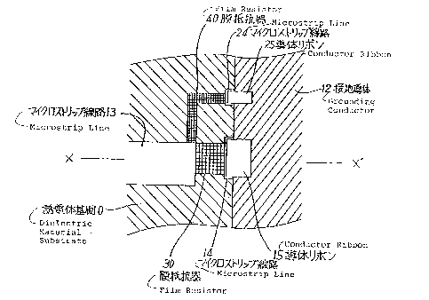
The first embodiment of the present invention is
shown in Fig. 6 and Fig. 7. Fig. 6 is a plan view of a
film resistance terminator as an embodiment of the
~2~
present invention and Fig. 7 is a sectional view along
the line X-X' in Fig. 6. The like elements are desig-
nated by the like reference numerals throughout the
drawings.
Moreover, Fig. 5 is given to explain input impe-
dances of the film resistors. In this figure, the
frequency is considered to 20 GHz which is largely
influenced by the reactance element. In this embodi-
ment, the inductive reactance element by the film
reistor can be cancelled by providing a film resistor
having the other capacitive reactance element. There-
fore, a film resistance terminator is formed through
the best combination which provides the desired value
of cmobined resistance value and a combined reactance
element close to zero by changing the length of the
film resistors in various sizes and drawing a plurality
of locie as shown in FigO 5.
Like the prior art, the present invention provides
a film resistor 40 having a capacitive reactance for
cancelling inductive reactance of the film resistor 30
to a film resistance terminator formed by the dielect-
ric material substrate 10 covered with a conductor film
11 at the rear surface, a grounding conductor 12,
microstrip lines 13, 14, a film resistor 30 and a con-
2~2~3 !~ 7~-
ductor ribbon 15. Moreover, the microstrip line 24 for
grounding the film resistor 40 and conductor ribbon 25
are further added.
Here, the dielectric material substrate 10 in this
embodiment is formed by alumina ceramic with specific
dielectric constant of 9.8 and thickness of 0.38 mm;
the microstrip line 13 is formed by a conductor with
width in the widht of 0.36 mm and thickness of 0.003
mm. The microstrip line 14 for grounding the film
resistor 30 has the width of 0.36 mm and length of 0.1
mm and this microstrip line 14 is grounded by the
conductor ribbon 15. The film resistor 40 newly added
has the width of 0.1 mm and length of 1 mm and the
microstrip line 24 for grounding such film resistor has
the width of 0.15 n~ and length of 0.1 mm. The area
resistivity of film resistor is 50 Q /square.
; For determination of above sizes, following graph
is generated. For instance, a graph indicating the
input impedances of the film resistors in the width of
0.3 mm, 0.15 mm and 0.1 mm calculated by inputting the
practical values to the formula (1) is shown in Fig. 5.
The horizontal axis of Fig. 5 denotes resistance
element (herein after referred to as Rin), while the
vertical axis, reactance element (hereinafter referred
-- 10 --
~2~
to as Xin)~ In the figure, a indicates an input
impedance of the film resistor in the width of 0.3 mm,
while b, that in the width of 0.15 mm and c, that in
the width of 0.1 mm. This graph is obtained by
plotting the impedances by changing the length of film
resistor in the step of 0.1 mm under the frequency of
20 GHz.
In the case of graph a in Fig. 5, when the length
is 0, both Rin, Xin are 0 ~ . When the length
increases, both Rin, Xin also increase at the
beginning. But, Xin is an inductive reactance element~
When Rin becomes almost 50Q , Xin reduces, on the
contrary. When Rin becomes almost 90 Q , Xin changes to
the capacitive reactance and increases. Moreover, Rin
reduces, on the contrary, from about 115Q , in
addition, the capacitive reactance Xin also reduces
from almost 70 ~ , Rin is converted almost to 75 ~ ,
while Xin is converged to almost 50 Q .
In the case of graph b in Fig. S, when the length
is zero, both Rin and Xin are 0 Q. When the length
increases, both Rin~ Xin increase at the beginning.
However, Xin is inductive reactance element. When Rin
bocomes about 70 Q, Xin reduces on the contrary. When
Rin becom~s almost 125 Q , Xin becomes capacitive
-- 11 --
2~2~7~
reactance and increases. Meanwhile, Rin reduces, on
the contrary, from about 160 Q and the capacitive
reactance Xin also reduces from about 110 Q and Rin is
converted to almost 120Q , while Xin to almost 95 Q .
In the case of graph c in Fig. 5, when the length
is zero, both Rin, Xin are 0 Q . When the length
increases, both Rin, Xin increase at the beginning.
However, Xin is inductive reactance element. When
Rin becomes about loOQ , Xin reduces on the contrary.
When Rin becomes almost 140 Q , Xin becomes capacitive
reactance and increases gradually. When Rin reches
about 220 Q, it gradually reduces on the contrary. In
addition, the capacitive reactance Xin gradually
reduces from about 150 Q and Rin is converged to almost
150 ~, while Xin to about 125 ~ .
As will be understood from the above graph, the
conventional film resistor 14 in this embodiment has
the width of 0.3 mm and the length of 0.3 mm.
Accordingly, it corresponds to the point al of the
graph a, while Rin is 54 Q and inductive reactance
element Xin is about 13~ . Moreover, the film resistor
24 has the width of 0.1 mm and the length of 1 mm.
Accordingl~ it corresponds to the point cl of the graph
c, while Rin is 180 Q and capacitive reactance element
- 12 -
2~2~7~
Xin is about 148~o In this case, the combined Rin,
Xin of a couple of film resistors can be expressed by
the follo~ing formula when the characteristic impedance
of film resistor 14 is (Rl + jXl) and the character-
istic impedance of film resistor 24 is (R2 + jX2).
(R, + j X, ) (R2 + j Xz )
R in+ j X in = ~ --
(R, ~ i X, ) + (Rz + i Xz
From calculation of above formula,
~in + jXin = 48-56 + j4.7
This is close to the desired resistance value,
indicating that the reactance element becomes close to
zero. Therefore, when the input signal is high
frequency, a return loss can be improved. The return
loss in the first embodiment of the above structure is
a little deteriorated than the conventional one in the
low frequency band as shown in Fig. 3s but is improved
more than that of conventional one in the high
frequency band. As a total, the return loss becomes
20 ds or more and total characteristic can be improved
from the conventional one.
In addition, when the length of film resistor 14
is increased to 0.33 mm by about 0.03 mm, the resist-
ance element becomes almost 50 . In this case, as
- 13 -
2~2~'7'~
shown in Fig. 3C, the return loss may be improved even
for the low frequency input signal.
A5 explained above, a film resistance terminator
providing good return loss can be obtained by drawing
locie for the film resistors of various sizes as shwon
in Fig. 5 and selecting the values resulting in the
combined reactance element more closed to zero and the
desired resistance value.
Next, a second embodiment of the present invention
will be shown in Fig. 8 and Fig. 9. Fig. 8 is a pLan
view of a film resistance terminator as the embodiment,
while Fig. 9 is a sectional view along the line B-B' ln
Fig. 8. Like the prior art, this embodiment comprises
a dielectric material substrate 10 covered with a
conductive film 11 at the rear surface thereof, a
grounding conductor 12, microstrip lines 13, 14 and a
conductor ribbon 15. Moreover, this embodiment has the
divided three film resistors 31, 32, 33 in place of the
conventional film resistor 30. The dielectric material
substrate 10 is formed by alumina ceramic having a
specific dielectric constant of 9.8 in the thickness of
0. 38 mm, the microstrip line 13 is formed by a
conductor in the width of 0.36 mm and thickness of
0.003 mm, the microstrip line 14 connecting the film
- 14 -
~$~
resistors 31, 32, 33 to the grounding conductor has the
width of 0.36 mm and length of 0.1 mm and this micro-
strip line 14 is grounded by the conductor ribbon 15.
The microstrip ~ines 31, 32, 33 have the width of 0.1 -~
mm and length of 0.3 mm.
In general, a resistance value R of the film
resistor is expressed as follow when the length of film
resistor is [mm], width is w [mm] and a resistivity
is ~ [~ mm].
R G ( ~ / t ) ( I / w )
R s ( 1 /w ) ( Q )
Rs = ( p/t )
~ ere, Rs is an area resistivity and when the
length and the width w of film resistor are constant,
the resistance value R ~epends only on the thickness t.
Meanwhile, when the thickness t is set to a
constant value, th~ àrea resistivity Rs also becornes
constant and a resistance value R depends on the legnth
and width w.
As shown in Fig~ 8, the present embodiment obtains
the desired resistance value as a combined resistance
value by narrowing the width of one film resistor and
- 15 -
. .
202~ 7~
increasing a resistance value of each film resistor by
dividing a film resistor into a plurality of sections
in the width direction and then connecting resistor
sections in parallel.
Details are explained hereunder. As will be
understood from the point c2 of graph c of Fig. 5, the
characteristic impedance of the film resistors 31, 32,
33 can be judged as follow from the sizes thereof that
Rin is about 150 ~ and Xin is capacitive and several
ohms. In this case, a total Rin of the film resistors
divided into three sections can be calculated as 50
and it has the desired serial resistance value like the
conventional one. On the contrary, the combined Xin
becomes very small in comparison with the conventional
one because each reactance element is several ohms.
Accordingly, deterioration of characteristic impedance
of the microstrip line 13 is also lowered even under
the high frequency band. Therefore, a measured return
loss of this embodiment can be considerably improved in
comparison with the conventional one as shown in Fig.
3D.
Moreover, an application example of the second
embodiment is shown in Fig. 10. In the terminator -
shown in Fig. 10, the microstrip line and conductor
- 16 -
2 ~ '7~
ribbon are also divided, in addition to the film
resistor, corresponding thereto and thereby the
microstrip lines 34, 35, 36 and conductor ribbons 26,
27, 28 are provided. In the second embodiment Xin of
the microstrip line 14 and conductor ribbon 15 is not
considered but the reactance element is decreased by
dividing the microstrip line 14 and conductor ribbon 15
like the film resistor. Accordingly, as shown in Fig.
3E, the return loss is more improved than the second
embodiment.
The present invention has been explained by refer-
ring to the embodiments thereof. However, the
microstrip line and grounding conductor may be connect-
ed electrically with a gold line in place of the
conductor ribbon. In addition, a number of divisions
of film resistor is not limited only to three sections
considering the sizes thereof and the film resistor may
also be divided into two sections. In this case, the
width of the one film resistor becomes O.15 mm. As
will be understood from the graph b of Fig. 5, the film
resistor has the characteristics that Rin is about 100
and Xin is inductive resistance and becomes about 8
Accordingly, the combined ~in of two film resistors is
having a serial resistance value similar to that of
2~2$3'~
conventional ~ilm resistor, while the combined Xin
becomes smaller than the conventional film resistor.
However, in case the film resistor is divided into
three sections, the reactance element becomes smaller
and it is effective means. As explained above, the
present invention is not limited only to such
embodiments.
rEffect of the Invention]
As explained previously, the present invention is
capable of reducing reactance element of film resistors
through employment of the structure for cancelling the
reactance element of the conventional film resistor and
the structure for dividing the film resistor. There-
fore, deterioration of impedance characteristic of
microstrip line 14 under the high frequency band may be
lowered. As a result, return loss can be improved and
sufficient termination can be realized even under the
high frequency band.
- 18 -