Note: Descriptions are shown in the official language in which they were submitted.
~0267 89
POWER FEED CIRCUIT FOR DIGITAL COMMUNICATIONS
TERMINAL EQUIPMENT
Field Of The Invention
The invention is in the field of power feed
5 apparatus and methods for supplying transmission line
connected terminals with energizing current. More
particularly the invention relates to apparatus and
methods for powering a digital signal telecommunications
terminal equipment wherein an initial power-up current
10 in-rush may exceed a normal load current by many times.
Background of the Invention
Traditionally a telephone terminal apparatus,
for example telephones and the like, is coupled through
an associated telephone line with a central power source
15 via a line interface circuit. The line interface circuit
includes circuitry, usually of a resistive nature, for
feeding energizing direct current from the central power
source to the telephone terminal apparatus. Recently,
various active line interface circuits have been
20 developed wherein the function of feeding the energizing
direct current is performed by active elements which may
optimize the coupling of the telephone with an associated
telephone system. Such active line circuits may include
over current protection circuitry which responds to
25 unintended operational faults, for example power line
crosses, short circuits or ground faults, by somewhat
limiting current flow in the interest of preventing
catastrophic failure of line interface circuit.
Recently telephone terminal apparatus of a
30 digital nature have been developed to take advantage of
the recommended Integrated Services Digital Network
(ISDN) standard. In ISDN jargon a terminal apparatus is
usually referred to as a terminal equipment (TE), a line
interface circuit as a network termination (NTl), and a
35 line for connection between a NTl and a TE as a terminal
q~
2026789
- (T) interface, hereafter referred to as a T bus. The TEs
are characterized by digital circuitry requiring an
operating voltage or voltages not conventionally
available from an associated telephone facility. However
5 the traditional reliability of telephony service is
nevertheless preferred. Hence one arrangement is
provided wherein a convenient physical location for a
group of NTls is also provided with a line power source,
which is intended to be more reliable than the supply
10 service expected from a local electrical utility. Each
of the NTls is provided with power from the line power
source, at a potential of about 50 volts, so that
energizing direct current is made available to each
associated TE via the wires of the interconnecting T bus.
15 A typical TE includes a direct current to direct current
DC to DC converter which utilizes between about 40 to 60
milliamperes of current from the T bus to provide the
required voltage or voltages for normal operation.
However initiation of operation of a TE, such as when it
20 is first plugged into a T bus or when power is initially
applied at the NTl, typically draws a momentary surge of
current. The surge of current is that which is required
to initiate operation of the typical DC to DC converter
and associated filter capacitors. In a normal power up
25 event in a TE, the DC to DC converter usually draws a
current peak or current inrush, which may exceed an
ampere for as much as ten milliseconds. In such
circumstances the typical current limiting circuit
intended to protect the typical line interface circuit is
30 inappropriate for operation throughout the whole current
load regime. For example, if a current limit of twice
the normal operating current is set, there will be
insufficient current for start up of the DC to DC
converter and on the other hand if a current limit
35 sufficiently great to accommodate start up is set, a
fault may be permitted to draw current for a period of
- 2026789
time sufficient to seriously jeopardize the operations of
the NT1, physically adjacent, and the line power source.
It is an object of the invention to supply
operating current from a central line power source via a
5 line interface circuit, to a terminal equipment having a
DC to DC converter, while providing an over current
protection feature which is effective across the entire
load current regime of the terminal equipment.
10 Summary Of The Invention
In accordance with the invention, a current
control apparatus is provided for supplying an energizing
direct current flow from a source of power via a
transmission line to a telecommunications terminal
15 apparatus being continuously operable while drawing a
load current which is exceeded by an inrush current being
greater than the load current at a moment of power up.
The current control apparatus is for connection in series
between the power source and the transmission line and
20 comprises: means for generating a magnitude signal being
representative of an amount of said energizing direct
current flow; means for generating a static control
signal for defining a maximum limit of load current;
means for generating a momentary dynamic control signal
25 for defining a maximum limit of the inrush current in
response to the magnitude signal increasing from a level
representative of less than the maximum limit of load
current to a level representative of more than the
maximum limit of load current; and switch means
30 responsive to the magnitude signal and the static and
dynamic control signals, to be set in an ON condition for
conducting said current flow, when either one of said
maximum limits is greater than the energizing direct
current as is instantly represented by the magnitude
35 signal, otherwise to be reset in an OFF condition, and
while in the OFF condition being responsive to an
4 2026789
apparent open circuit condition of the transmission line
to become set in the ON condition.
In one example, a line interface circuit
couples energizing direct current, from a line power
5 supply to a communications line, for operation of a
telecommunications terminal apparatus. The line
interface circuit comprises: first and second power
terminals for connection to the line power supply; first
and second line terminals for connection to the
10 communication line; and a current control means, being
connected between a one of the first and second power
terminals, and a respective one of the first and second
line terminals, for conducting the energizing direct
current therebetween, for temporarily isolating the power
15 terminal from the line terminal to stop an inrush current
in excess of a dynamic limit, and permanently isolating
the power terminal from the line terminal to stop a load
current in excess of a static limit, until a virtual open
circuit condition occurs across the first and second line
20 terminals.
Also in accordance with the invention a method
is provided for supplying an energizing direct current
flow, from a source of power via a transmission line to a
telecommunications terminal apparatus, said terminal
25 apparatus being continuously operable while drawing a
load current which is exceeded by an inrush current being
greater than the load current at a moment of power up.
The method comprising the steps of:
a) generating a magnitude signal being
30 representative of an amount of said energizing direct
current flow;
b) generating a static control signal for
defining a maximum limit of load current;
c) generating a momentary dynamic control
35 signal for defining a maximum limit of the inrush current
in response to the magnitude signal increasing from a
level representative of less than the maximum limit of
2026789
load current to a level representative of more than the
maximum limit of load current;
d) in response to the magnitude signal and the
static and dynamic control signals, providing a path with
5 an impedance of less than a first value suitable for
conducting the energizing current flow, when either one
of said maximum limits is greater than the energizing
direct current as is instantly represented by the
magnitude signal, otherwise increasing the impedance of
10 said path to a second value greater than the first value
and unsuitable for conducting the energizing current
flow; and
e) while said path is of at least the second
impedance value and in an event where the transmission
15 line appears to be an open circuit, reducing the
impedance of the path to less than the first value.
Brief DescriDtion Of The Drawin~s
An example embodiment is described with
20 reference to the accompanying drawings in which:
Figure 1 is a block schematic diagram of a
telecommunications facility and a network termination
equipment group for coupling terminal equipment thereto;
Figure 2 is a block schematic diagram of a line
25 interface circuit, used in the network termination
equipment group shown in figure 1 in accordance with the
invention;
Figure 3 is a schematic diagram which
illustrates a detailed example of a current switch used
30 in the line interface circuit illustrated in figure 2;
Figure 4 is a schematic diagram which
illustrates a detailed example of a dynamic reference
generator used in the line interface circuit illustrated
in figure 2;
Figure 5 is a schematic diagram which
illustrates a detailed example of a static reference
generator used in the line interface circuit illustrated
in figure 2; and
-
2~126789
Figures 6 and 7 are graphical representations
of current limiting events which may occur during
operation in accordance with the invention of the
interface circuit as illustrated in figures 2 to 5.
Descri~tion of the ExamDle Embodiment
Figure 1 illustrates a typical connection of
several terminal equipments (TE) shown at 13 and 130.
Each TE has associated with it a DC to DC converter, 15
10 and 150 respectively. Each TE is connected to a
telecommunications facility 100 via a U interface 101.
The U interface 101 is a digital signals link which
typically conforms to a telephony standard such as the
well known TlEl transmission standard. The U interface
15 101 transports signals between the telecommunications
facility 100 and a network termination equipment group 8.
These signals are distributed on a predetermined basis
across a group of network terminations (NTl) shown at 8a
through 8n. A battery power source 20 supplies
20 termination equipment power for operation of each of the
NTls 8a through 8n, and in this example supplies line
power for the operations of the TEs 13 through 130, via
positive and negative power terminals 22 and 21
respectively. Each of the NTls is connected via a group
25 of leads 10 as illustrated with respect to the terminal
equipment 13. This is usually a transformer connection
as is illustrated by transformer windings 11 with sending
terminals Sl and S3 and receiving terminals S2 and S4
connected to a 4 wire T bus 14, as shown. Power
30 terminals at P9a and P9b are connected to centre taps 16
and 17 of the transformer windings 11 in a well known
phantom power feed arrangement. In like manner the TE
130 is connected via a T bus 140. In an alternate
arrangement, not shown, an additional two wires may be
35 provided in the T bus to separately power the TE via the
terminals P9a and P9b. In the alternate arrangement the
7 2026789
transformer 11 is spared the chore of having to conduct
dc current via its winding portions.
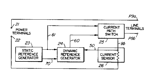
Each of the NTls includes a line interface
circuit for coupling current from the power source 20,
5 hereinafter referred to as the line power supply 20, to
its associated T bus. The line interface circuit is
generally illustrated in Figure 2. In Figure 2, the
positive power terminal 21 is connected directly to the
line terminal P9a. However the negative power terminal
10 22 is connected via a current sensor 26, a current path
9b, and a current path switch 25 to the line terminal
P9b. A static reference generator 23 provides a negative
voltage reference on a lead 70 for use by a dynamic
reference generator 24. The static reference generator
15 23 also provides a stable voltage supply on a lead 61 for
use by the dynamic reference generator 24 and the current
path switch 25. The dynamic reference generator 24 is
provided with a sense signal on a lead 50 connected from
the current sensor 26. The dynamic reference generator
20 uses the signals on the lead 70 and 50 to generate a
control signal on a lead 60 for use by the current path
switch 25. The current path switch is required to
provide a current path which at any one time is of a very
low impedance, or alternately is of a much higher
25 impedance, in accordance with dynamics of the ongoing
operation of the NTl and any TE connected thereto.
Operation of the line interface circuit is
discussed in more detail with reference to Figures 3, 4
and 5.
Referring to Figure 3, a differential amplifier
31 includes an open collector output connected as shown
with a resistor 32, a capacitor 35 and a zener diode 36
to control conduction of energizing current for an
associated TE via an enhancement mode field effect
35 transistor (FET) 41. The FET 41 is connected as part of
the current path 9b in series between a diode 46 and a
current sensing device in this case a resistor 40, as
~. ~^
-
8 2~78~
- shown. An initializing circuit path 9c includes a FET 42
connected as shown with resistors 43 and 45 and a
capacitor 44. An inverting input of the differential
amplifier 31 is connected with a capacitor 33, a resistor
5 34 and the FET 42. A non-inverting input of the
differential amplifier 31 is connected to receive a
control signal. While the FET 42 is ON, the current path
9c in combination with the resistor 34 establishes a
positive feedback path from a junction of the resistor 40
10 and the FET 41, to the inverting input of the
differential amplifier 31. A secondary current path 9d
is provided by a resistor 48 connected in series with a
diode 49 and the diode 46. When the FET 41 is switched
OFF as in response to an over current condition, the
15 secondary current path 9d provides a small trickle of
current which flows via the terminals P9a and P9b when
these terminals are other than effectively open
circuited. In an event wherein the trickle current ceases
to flow the FET 41 may be returned to the ON condition.
20 The circuit, so arranged, is operable to maintain the FET
41 in an ON condition as long as the voltage at the
inverting input is less positive than the voltage of the
control signal at the non-inverting input of the
differential amplifier 31.
The dynamic reference generator in Figure 4
includes a differential amplifier 51 having an inverting
input and a non-inverting input. The differential
amplifier 51 in this example includes an open collector
output connected as shown to a series arrangement of
30 resistors 52 and 54 and a capacitor 53. A junction of
the resistor 54 and the capacitor 53 is connected to an
anode electrode of a diode 56. A cathode electrode of a
diode 56 is connected to a junction of resistors 57 and
58 arranged in series.
The static reference generator, in figure 5, is
used to provide a stable supply voltage supply -Vl and a
reference voltage V REF-. The static reference generator
-
9 2026789
is shown to be connected across the power terminals 22
and 21 to receive current across a potential +V, -V from
the battery power source. A resistor 62 is connected as
shown in a shunt combination with a voltage regulator 63
5 to provide the intermediate voltage -Vl on a lead 61. In
this case, the intermediate voltage -Vl is about 10 volts
more positive than the potential -V. Resistors 65, 66
and 67 are connected in series and provide a controlled
potential at a first voltage tap 63t for operation of the
10 voltage regulator 63. A second voltage tap provides a
voltage V REF- which is about a volt more positive than
the potential -V. Capacitor 68 and 64 provide filtering.
Operation of the dynamic reference generator 24
shown in Figure 4 is as follows. With reference to the
15 differential amplifier 51, assuming that its inverting
input is more positive than its non-inverting input, its
output then assumes a potential near that of -V.
Alternately in an event where the sense voltage (50)
becomes greater than the potential of V REF-, the output
20 of the differential amplifier 51 becomes a high
impedance. Hence a positive going pulse, with an edge of
near 10 volts with respect to -V, is coupled across the
capacitor 53. The amplitude of the pulse edge is
determined by ohmic values of the resistors 52 and 57 in
25 a voltage divider arrangement. Following the pulse edge,
a falling or decay portion is characterized by the RC
value of the capacitor 53 and the resistors 57 and 52.
The pulse is transmitted via the diode 56 until its
amplitude approaches to within the forward voltage drop,
30 of the diode 56, with respect the normal voltage at a
junction 60t. As time passes, the potential of the
pulses further reduced and the diode 56 becomes non-
conductive. Of course, if at any time during the decay
portion the sense signal becomes less than the potential
35 of V REF-, the output of the differential amplifier 51
swings toward the -V potential, thereby terminating the
pulse. While the pulse is terminating, a capacitor 59
- 2~2~78~
- 10
- extends and smooths the terminating portion of the pulse.
If however the sense signal again rises in a few moments,
the pulse is reinitiated with an amplitude reduced by an
amount generally as characterized by said RC value. The
5 resistor 54 discharges the capacitor 53 when the pulse is
terminated such that after about five or more time
constants a full amplitude pulse will be generated. This
is illustrated in figure 6 and figure 7 wherein figure 6
shows a typical continuous pulse, and figure 7, shows an
10 interrupted pulse. The control signal at the output 60
is therefore a static level as determined by the
potential at the junction 60t, unless the potential is
over-ridden by the dynamic level switched via the diode
56 to the output 60.
Referring to figure 3, the current path switch
operates in response to a sample of the voltage sensed
across the resistor 40 and the control signal provided on
the lead 60. In an event where power is first applied
across the power terminals 21 and 22 from the line power
20 supply 20 as illustrated in Figure 1, the FET 42 is
initially maintained in an OFF condition by voltage at
the junction of the capacitor 44 and the resistor 43.
This voltage rises in accordance with the RC time
constant of these elements toward the potential -Vl to
25 switch the FET 42 into the ON condition which persists
during the rest of the circuit function, as long as power
is not interrupted. Hence positive feedback, normally
coupled via the current path 9c, is suppressed for the
moment shortly after the initial power application at the
30 power terminals 21 and 22, to prevent a premature locking
of FET 41 into a permanent OFF state, that is before all
operating static voltages have stabilized. The inrush of
current generates a very much more positive voltage on
the sense lead 50 which causes the dynamic reference
35 generator to generate a positive going pulse control
signal, which in turn tends to maintain the FET 41 in the
ON condition. Voltage appearing at the inverting input
`~ 2026789
11
of the differential amplifier 31 is developed across the
resistor 40 and the capacitor 33 and rises in accordance
with the RC time constant of the resistors 34 and 40 and
capacitor 33, so that the differential amplifier 31 is
5 prevented from responding too quickly to the rising
amplitude of the sensed current in the current path 9b.
This permits the control signal pulse to be generated
before it is compared to the sensed current by the
differential amplifier 31. If the sensed inrush of
10 current does not exceed the permissible level as set by
the control signal, the FET 41 is maintained in the ON
state. However, if the sensed current exceeds the
control signal permissible level, the FET 41 is
controlled by the differential amplifier 31 to be in a
15 less conductive state. This causes a rise in the voltage
level in the path 9c which is impressed upon the
inverting input of the differential amplifier 31 and
thereby causes the FET 41 to be locked OFF. While the
FET 41 locked OFF, the trickle current may be conducted
20 via the current path 9d. This condition is maintained
until an effective external open circuit condition is
established across the terminals P9a and P9b. The open
circuit condition, indicated by an absence of the trickle
current, is characteristic of the impedance presented at
25 the power feed terminals of a typical DC to DC converter
in the event it has failed to function due to
insufficient voltage supply. The diode 49 may be of a
light emitting type to give a visual indication of an
occurrence of the trickle current. In the event that the
30 open circuit condition is established, the trickle
current fails to flow on the path 9d and hence the
voltage in the path 9c tends toward the -V level. In
this case the differential amplifier 31 again switches
the FET 41 ON, into the conduction state.
Figures 6 and 7 show the extremes of wave
shapes which the control signal in the lead 60 may
assume. These wave forms are presented in terms of the
- - 2`02678~
12
dynamic current characteristics of the circuit as these
would be sensed across the resistor 40, in Figure 3.
Referring to Figure 6, current is shown on a vertical
axis and time is represented on the horizontal axis.
5 Assuming an inrush of current at the power terminals P9a
and P9b, the maximum permissible limit rises abruptly to
a peak whereafter the limit is reduced exponentially in
accordance with the RC time constant previously discussed
in relation to Figure 4. If however the current demand
10 at the terminals P9a and P9b falls to less than the
static threshold as determined by the V REF- potential on
lead 70, then as shown in Figure 7, the maximum permitted
current returns to the normal operating current level.
If however the apparatus during start up requires several
15 inrushes, the maximum permitted current will return to a
high point of slightly more than the current which was
permitted just before the envelope returned to the normal
load current level. This may happen several times, as
may be peculiar to the particular terminal equipment
20 being connected to the line.
As before mentioned, Figures 6 and 7 show the
extremes of operation, however there are various
scenarios which are not illustrated here as these will be
observable by a person having constructed and used the
25 invention.
The illustrated embodiment is achieved by a
combination of analog circuit elements. However, it will
be apparent to persons of typical skill in the electronic
arts that the functionality of the invention may also be
30 achieved by means of a suitably interfaced and programmed
digital controller or microcomputer, a binary output of
which may be used to control the FET 41 in place of the
amplifier 31 and the circuits illustrated in the figures
4 and 5.