Note: Descriptions are shown in the official language in which they were submitted.
20269 1 6
AUDIO AMPLIFIER LIN~ FOR
A R~MOTE POWER AMPLIFIER
The present invention relates in general to
audio systems which prevent distortion from amplifier
clipping by employing voltage limiting, and more
specifically to automotive audio systems in which power
amplification of an audio signal is performed in a
location remote from a main audio unit.
Typical audio reproduction systems include a
10 variable-gain preamplification stage followed by a
fised-gain power amplifier which drives an output
transducer such as a speaker. A volume control voltage
provided to the variable-gain stage controls the output
volume heard by a listener.
An important objective in designing an audio
system is to provide minim~lm distortion in signal
reproduction. However, there is always some distortion,
especially at high sound levels. As the magnitude of the
signal provided from the variable-gain preamplifier stage
20 to the power amplifier increases above a certain level,
the power amplifier becomes overdriven. This situation
occurs when the input signal to the power amplifier
multiplied by the fised-gain of the power amplifier
approaches the supply voltage provided to the power
25 amplifier. As a result, the power amplifier becomes
saturated and the signal peaks of the audio signal are
distorted by clipping. The variable-gain preamplifier is
also susceptible to clipping, but the power amplifier is
likely to begin clipping first.
The problem of clipping is severe in automotive
audio systems. Less voltage headroom ~i.e., safety
margin) is available to the power amplifier since the
automobile is limited to a 12-volt electrical supply.
S~
f~.
2026916
Although a DC/DC converter can be used to obtain a higher
DC voltage, such converters are relatively expensive.
Also, bass boost is needed in the automotive environment
to mask low frequency road and engine noise, making
clipping more likely.
High performance automotive audio systems
typically employ a power amplifier located remote from
the main audio unit in the dashboard, where it is not
visible to the occupants of the automobile. A remotely
located power amplifier saves space in the dashboard and
reduces the amount of heat that would otherwise be
generated in the main unit.
When the two amplifier stages are not located
together, the problem of clipping of each amplifier stage
has been handled individually in the prior art.
Therefore, either one or both amplifier stages have been
provided with voltage limiting in order to reduce
distortion from signal clipping.
In a voltage limiting amplifier, whenever the
amplifier output exceeds a predetermined referenced
voltage, the input signal to that amplifier stage is
attenuated in order to ensure that the amplifier is not
overdriven. In the prior art remote power amplifier
systems, unless both the variable-gain amplifier in the
main unit and the power amplifier in the remote unit are
separately provided with voltage limiting, clipping
distortion can result at sufficiently high input signal
levels or gain levels, and once distortion is introduced
into the signal it cannot be removed.
An audio system employing voltage limiting
amplifiers in both the main variable-gain preamplifier
and the remote power amplifier avoids clipping
distortion, but at the expense of an additional source of
distortion referred to as modulation-type distortion.
The gain reduction elements employed in the voltage
~ 2026~ ~ 6
_ 3
limiting feedback circuits nec~ss~rily have time
constants characteristic of their operation.
Specifically, there are attack times and release times
which govern the gain reduction. It is relatively
difficult and eYpencive to provide perfectly matched
attack and release times in the two independent
limiters acting in series, and any mismatch in attack
and release times creates distortion in the audio
signal.
The present invention is directed towards
elimination of clipping distortion from an audio system
without introducing any new source of distortion, in
particular to the provision of clipping protection for
an audio system including a main chassis having a
preamplifier and a remote stage having a power
amplifier.
The present invention also is directed to the
provision of a method for preventing distortion in an
audio system and for preventing clipping in both a main
chassis preamplifier and a remote stage power amplifier
without introducing modulation type distortion caused
by unmatched attack and release times.
According to the present invention, a voltage
limiting amplifier arrangement is employed in which the
output of the remote power amplifier is monitored to
detect the onset of clipping. However, the gain of the
power amplifier itself is not altered in response to
the detection of clipping. Rather, a clipping feedback
signal is provided from the remote clipping detector to
a gain reduction circuit which operates on the main
chassis preamplifier. This substantially eliminates
clipping problems for both amplifiers. However, it may
also be desirable to provide a second clipping detector
to monitor the output of the preamplifier. This second
clipping detector activates the same gain reduction
circuit.
i, ,
," .~
2026~ 1 6
More specifically, the present invention, in one
aspect, provides an audio system for amplifying an
audio signal comprising a main chassis, an audio line,
and a remote amplifier stage. The main chassis
includes preamplifier means for amplifying the audio
signal and gain control means coupled to the
preamplifier means for reducing the magnitude of the
audio signal at the output of the preamplifier means in
response to a gain reduction signal. Preferably, the
reduction of the preamplifier output is achieved by
attenuating the preamplifier input. Alternatively, the
reduction can be achieved by lowering the gain factor
of the preamplifier. The audio line transmits the
audio signal from the preamplifier means to the remote
amplifier stage. The remote amplifier stage includes
power amplifier means coupled to the audio line for
amplifying the audio signal by a substantially fixed-
gain. It also includes first clip detector means
coupled to the output of the power amplifier means for
generating a gain reduction signal whenever signal
clipping occurs in the remote amplifier stage.
Preferably, the audio system further includes a control
line for transmitting the gain reduction signal from
the first clip detector to the gain control means.
Furthermore, the main chassis may further include
second clip detector means coupled to the output of the
preamplifier means for generating its own gain
reduction signal whenever signal clipping occurs in the
preamplifier means. Thus, clipping distortion is
eliminated by provision of voltage limiting while
modulation-type distortion is avoided since there is
only one attack and one release time introduced into
the circuit (there being only one gain reduction
element).
In another aspect of the present invention, there
is provided a method of preventing distortion in an
audio system including a preamplifier on a main chassis
-2026q 1 ~
_ 5
providing an audio signal to a remote amplifier stage,
the method comprising the steps of detecting the onset
of clipping in the remote amplifier stage; conducting a
signal from the remote amplifier to the main chassis to
indicate the onset of clipping; and reducing the
magnitude of the audio signal in the main chassis in
response to the signal, whereby clipping in the remote
amplifier is prevented.
The novel features of the invention are set forth
with particularity in the appended claims. The
invention itself, however, both as to its organization
and method of operation, together with further
advantages thereof, may best be understood by reference
to the following description taken in conjunction with
the accompanying drawings, in which:
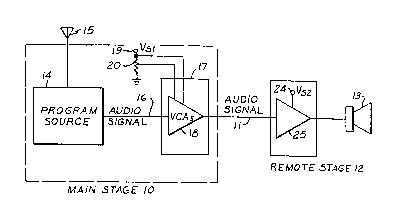
Figure 1 is a block diagram showing an audio
system having a remote power amplifier as is used in
the present invention;
Figure 2 is a waveform diagram illustrating the
occurrence of signal clipping;
Figure 3 is a schematic diagram showing a typical
voltage limiting circuit;
Figure 4 is a part schematic, part block diagram
showing a preferred embodiment of the voltage limiting
circuit of the present invention;
Figure 5 is a schematic diagram showing a clip
detector circuit of the present invention in greater
detail; and
Figure 6 is a schematic diagram of a clip detector
employed in the remote amplifier stage of the present
invention.
Referring to Figure 1, a main chassis 10 transmits
an audio signal on an audio line 11 to a remote stage
12. The audio signal may typically include front and
rear stereo signals for a total of four separate
si,gnals. Audio line 11 would then include four
S~,
, ~ ; ~
20269 1 6
5a
separate signal lines. Remote stage 12 drives a
speaker 13.
Main chassis 10 includes a program source 14 which
preferably includes a radio tuner connected to an
antenna 15, a cassette tape player, a CD player, or the
- 2026916
-- 6 --
like. An audio signal is provided from program source 14
over an audio line 16 to a voltage controlled amplifier
(VCA) 18. Although four audio signals may actually be
present, a single audio line 16 is shown for simplicity
of e2planation. VCA 18 is preferably included as part of
a tone/volume control integrated circuit 17, such as the
TDA1524A integrated circuit manufactured by Philips. A
supply voltage Vsl is provided to a terminal 19.
Terminal 19 is connected to a power supply input of VCA
18 and to a grounded potentiometer 20. The adjustable
tap of potentiometer 20 is connected to a volume control
input of VCA 18 for controlling the signal gain provided
by VCA 18.
The audio signal provided by the output of VCA
18 is transmitted over audio line 11 to the input of a
power amplifier 25 in remote stage 12. Power amplifier
25 is connected to supply voltage Vs2 provided at a
terminal 24.
VCA 18 may preferably include separate amplifier
sections for controlling wideband volume and relative
bass and treble levels. In operation, the audio signal
provided by program source 14 is amplified by VCA 18
according to a volume control voltage provided by
potentiometer 20 and according to tone control voltages
provided by other potentiometers (not shown). The
amplified audio signal provided on line 11 to power
amplifier 25 is amplified by a fixed-gain to drive
speaker 13.
Figure 2 illustrates how clipping could occur at
the outputs of either the main chassis VCA 18 or power
amplifier 25. The output of a DC amplifier can swing
between voltage values of zero and the supply voltage
Vs to the amplifier. An audio signal waveform 26
oscillates around a bias point of the amplifier that is
generally midway between zero and the supply voltage.
~026~16
-- 7 --
Whenever the audio input signal to the amplifier times
the amplifier gain equals a value outside the maximum
amplifier swing, the waveform is clipped at 27 rather
than following its ideal path 28.
In order to prevent clipping, an amplifier
voltage limiting feedback circuit can be employed, as
shown in Figure 3. An amplifier 30 receives an audio
input signal on an input line 31 and provides an
amplified audio output signal on an output line 32.
Amplifier 30 is provided with a supply voltage Vs.
Output line 32 is connected to the noninverting input of
a comparator 33. The inverting input of comparator 33 is
connected to a reference voltage REF which is a positive
voltage that is just slightly less than supply voltage
Vs. The output of comparator 33 is connected to a
control input of a variable impedance or variable
attenuator 35 which provides a controlled resistance
between input line 31 and ground.
In operation, amplifier 30 provides an
amplification gain factor to an audio signal input on
line 31. Whenever the gain factor applied by amplifier
30 results in an output signal on line 32 having an
amplitude greater than the reference voltage REF on line
34, the output voltage supplied by comparator 33 switches
to a high level to indicate the onset of clipping. The
high voltage level generated by comparator 33 provides a
control signal that is integrated by attenuator 35
according to its attack and relaease times. Attenuator
35 reduces its variable resistance such that a portion of
the input signal on line 31 is shunted to ground, thereby
reducing the input signal to amplifier 30 and the
magnitude of the output signal provided on line 32.
Thus, the amplifier gain provided by the combination of
the amplifier and the voltage limiting circuit is
automatically adjusted to an amount which is at a maximum
20~6916
-- 8 --
with no clipping, subject to proper selection of attack
and release times of the attenuator circuit.
The attack time is the amount of time required
before the gain reduction circuit responds to an
overdrive condition. Release time is the lag between the
disappearance of an overdriving input condition and the
return of the variable attenuator to its maximum
impedance state. Although attack and release times are
unavoidable and can be beneficial, it has not been
possible to conveniently match attack and release time in
individual limiting circuits operating in series used in
the prior art.
The improved amplifier configuration of the
present invention shown in Figure 4 employs a single
attenuator 35 connected to the input of main chassis VCA
preamplifier 18. Attenuator 35 is controlled according
to the outputs of both main chassis VCA 18 and remote
power amplifier 25. A comparator 40 has its noninverting
input connected to the output of amplifier 25, in remote
stage 12, and has its inverting input connected to
reference voltage REF2. The output of comparator 40 is
connected to attenuator 35 via a control line 41 running
from remote stage 12 to main chassis 10.
Another comparator 51 is located in main chassis
10 and has its noninverting input connected to the output
of VCA 18. Its inverting input is connected to its own
reference voltage REFl. The output of comparator 51 is
connected to control line 41. Control line 41 is
connected to the base of a transistor 42 in attenuator
35. The base of transistor 42 is also connected to a
biasing network comprising a resistor 43 in parallel with
the series combination of a resistor 44 and a capacitor
45 to ground. The collector of transistor 42 is
connected to the cathode of a light emitting diode (LED)
47. The anode of LED 47 is connected to terminal 46
2026916
g
where voltage Vs is supplied. The emitter of
transistor 42 is coupled to ground through a resistor
48. A light dependent resistor (LDR) 50 is connected
between input line 16 and ground. LED 47 and LDR 50 are
located in close proximity or are joined by a light
transmitting path whereby light emitted from LED 47
causes a predetermined reduction in the resistance of LDR
50. In operation, comparators 40 and 51 generate a
relatively high voltage on (or supply a current to)
control line 41 upon the onset of clipping in their
respective amplifiers. The high signal on line 41
charges capacitor 45 through resistor 44 until the
turn-on voltage of transistor 42 is reached and
transistor 42 conducts. When the outputs of the
comparators both return to a low voltage, capacitor 45
discharges through resistors 43 and 44, eventually
causing transistor 42 to become nonconductive. Thus,
resistors 43 and 44 and capacitor 45 provide a desired
attack and release time for the limiting function.
When transistor 42 is biased into a conducting
state, current flows through LED 47 which generates
light. The light is directed to LDR 50, thereby
decreasing the resistance of LDR 50. The decreased
resistance of LDR 50 shunts a portion of the input signal
on line 16 away from VCA 18 and to ground. This results
in a reduced output from VCA 18. The output of power
amplifier 25 is also reduced since its input from VCA 18
was reduced.
The input signal to VCA 18 is attenuated in
response to clipping occurring in either VCA 18 or power
amplifier 25. The amount of attenuation provided by
attenuator 35 is sufficient to eliminate clipping of
either or both amplifiers. However, it may, in some
instances, be desirable to eliminate comparator 51 and to
attenuate the input signal to VCA 18 in response only to
2026916
-
-- 10 --
clipping in power amplifier 25 since power amplifier 25
typically enters a clipping condition before VCA 18 does.
The output of VCA 18 in tone/volume control
integrated circuit 17 typically comprises four channels,
including left-front (LF), right-front (RF), left-rear
(LR), and right-rear (RR). These channels are shown in
the clip detector circuit of Figure 5.
In order to derive the instantaneous peak
voltage on any individual channel, all channels feed into
comparator 51 from a common point 64. The audio signal
on LF is coupled to point 64 through a resistor 55 and a
forward-connected diode 56. The audio signal on RF is
coupled to point 64 through a resistor 57 and a
forward-connected diode 58. The audio signal on LR is
coupled to point 64 through a resistor 60 and a
forward-connected diode 61. The audio signal on RR is
coupled to point 64 through a resistor 62 and a
forward-connected diode 63. Common point 64 is connected
to the base of an NPN transistor 65 in comparator circuit
51. The emitter of transistor 65 is connected to the
junction of a pair of voltage dividing resistors 67 and
68 which divide the 10 volt supply voltage at terminal
46. The collector of transistor 65 is connected to a
resistor 70 which is also connected to terminal 46. The
collector of transistor 65 is also connected to the base
of a PNP transistor 71. Transistor 71 has its emitter
connected to terminal 46 and its collector connected to
the anode of a diode 72. The cathode of diode 72 is
connected to line 41.
In operation, the peak voltage appearing on
point 64 from all the channels is compared to the emitter
voltage of transistor 65 which is determined by the
voltage divider comprising resistors 67 and 68. Thus,
the reference voltage is a percentage of the 10-volt
supply voltage. When the peak voltage from any audio
2026!~1~
channel exceeds the reference voltage plus the turn-on
threshold of transistor 65, transistor 65 enters a
conducting state thereby reducing the voltage at its
collector. Thus, the base voltage of transistor 71 is
reduced to a point where transistor 71 also conducts.
The current through transistor 71 passes through diode 72
and charges the attenuator capacitor as previously
described.
Comparator circuit 40 shown in Figure 6 is
employed in remote amplifier stage 12. The four audio
signals of the power amplifier are respectively coupled
to a summing point 84 through resistors 75, 77, 80, and
82, correspondingly connected with forward-connected
diodes 76, 78, 81, and 83, as shown. Summing point 84 is
connected to the base of an NPN transistor 85 in
comparator circuit 40. The emitter of transistor 85 is
connected to the junction of a pair of voltage dividing
resistors 87 and 88 which divide the 12 volt supply
voltage of the remote power amplifier stage at terminal
86. The collector of transistor 85 is connected to a
resistor 90 which is also connected to terminal 86. The
collector of transistor 85 is also connected to the base
of a PNP transistor 91. Transistor 91 has its emitter
connected to a resistor 92 which is also connected to
terminal 86. The collector of transistor 91 is connected
to line 41.
Whenever the peak voltage from a power amplifier
channel at summing point 84 exceeds the reference voltage
provided by the voltage divider of resistors 87 and 88,
plus the turn-on threshold of transistor 85, transistors
85 and 91 enter their conducting states and a high output
signal results on control line 41. The high signal on
line 41 then causes a reduced gain in the main chassis
preamplifier as previously described.
Although a variable attenuator has been shown in
- 2026gl~
~ - 12 -
the preferred embodiments hereof, gain reduction of the
main chassis preamplifier could be achieved by directly
manipulating the gain factor of the preamplifier. For
example, a preamplifier can be used having a gain factor
controlled by a digital value written by software to a
control associated with the preamplifier. The TDA7306
integrated circuit manufactured by SGS-Thomson
Microelectronics provides such a preamplifier.
While preferred embodiments of the invention
have been shown and described herein, it will be
understood that such embodiments are provided by way of
example only. Numerous variations, changes, and
substitutions will occur to those skilled in the art
without departing from the spirit of the invention.
Accordingly, it is intended that the appended claims
cover all such variations as fall within the spirit and
scope of the invention.