Note: Descriptions are shown in the official language in which they were submitted.
~ ~ f~ Pl
--1--
CABLE CONNECTOR WITH A LOW INDUCTANCE PATH
The specification describes a cable connector and
more particularly, a cable connector with a low
inductance signal return path.
A known cable connector is disclosed in U.S.
Patent 4,602,831 and comprises, a housing block and an
electrical cable having at least one signal wire
connected to a corresponding signal contact on the
housing block, and at least one referencs wire of the
cable for connection to a reference electrical
potential. The signal wires transmit electrical
signals, either electrical power or electrical encoded
signals. The reference electrical potential is ground
voltage. Along the cable a reference conductor shields
the signal wires ~rom undesired influence, such as
electrostatic and electromagnel:ic coupling. In one form
of cable, the reference conduc1:or is a conductive shield
that encircles a corresponding signal wire. A re~erence
wire in contact With the shielcl connects to the
connector and to a reference e1ectrical potential
present in the connector.
As the switching speeds of the signals becoma
faster, there is a need for the signal contacts to
become closer together, to shorten signal transmission
paths between signal contacts, and to reduce an
allocation of valuable space to be consumed by the
contact spacing. The signal contacts are too close if
l4676 CA
~ . . .
2 ~ 7
--2--
they couple inductively and electrostatically, and
produce cross talk and impedance mismatch.
As the switching speeds of the signals become
faster, a further need exists to provide a low
inductance return path in the connector, to control
common impedance noise generation, and to establish
coupling of each signal contact electromagnetically and
electrostatically to the return path that is stronger
than a similar coupling to other signal conductors, and
to provicle an impedance that matches the impedance of
other parts of alectrical circuits transmitting the
signals, in order to reduce signal reflections.
However, such a return path in the connector consumes
additional space, and imposes a limit upon the closeness
of the signal contacts Thus a choice is presented,
whether to eliminate a return path and risk undesired
impedance mismatch and undesired coupling, or whether to
provide adequat2 return paths and sacrifice valuable
space to be consumed by increasing the contact spacing
and by enlarging the connector.
A feature of the invention resides in a cable
connector comprising, a housing coupled to a housing
block and receiving a signal contact on the housing
block in one of multiple contact positions in the
housing, a reference contact being received in the
housing and being connected to the reference conductor,
and the reference conductor extending in the housing and
14676 CA
--3--
beside each one of the multiple contact po~itions. An
advantage of the invention i5 that the reference
conductor extends a low inductance signal return path
into the housing and beside each signal contact received
in a corresponding one of the contact positions.
Another advantage of the invention is that the multiple
contact positions can be c10s2 togetherf since they
provide multiple choices for spacing apart signals that
would be too close together if routed to directly
adjacent contact positions. Another advantage of the
invention resides in a cable connector that combines
close together signal contact positions with a low
inductance signal return path extending from a housing
block to a housing and beside contact positions in the
housing.
According to the known cable connector disclosed in
U.S. Patent 4,602,831 ~ronts of the signal contacts
extend beyond a ~ront of a ground contact and thereby
lack coupling to an adjacent low inductanc~ signal
return path.
Another ~eature of the invention resides in a cable
connector having a reference conductor that extends
uncovered along a housing block for nesting dixectly
against another housing block on which are additional
signal contacts. The advantaqes are, that the housing
blocks are close together, and the signal contacts on
the housing blocks are directly ad~acent and close
14676 C~
-4~
together without undue coupling with one another,
because the reference conductor provides a common return
path for signal contacts on one housing block, and
provides a shield for each signal contact on the one
housiny block from each signal contact on the adjacent
housing block.
The invention will now be described by w~y of
example with reference to the accompanying drawings.
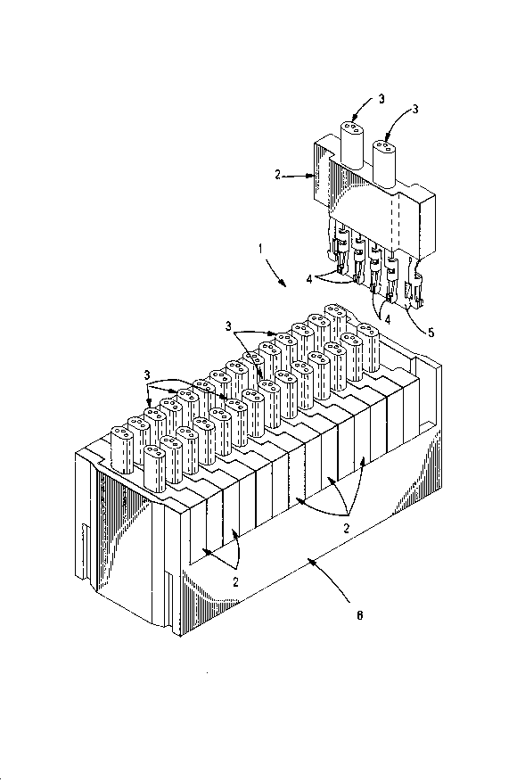
In the drawings, Figure 1 is a perspective view
with parts exploded of a cable connector.
Figure 2 is a plan view of a cable terminated with
a housing block and electrical signal contacts and an
electrical reference conductor.
Figure 3 is a side view o~ the structure shown in
Figure 2.
Figure 4 is an end view o~ the structure shown in
Fiqure 2 together with a duplicate of the structure.
Figure 5 is a perspectiv2 view of a housing.
Figure 6 is a ~ragmentary plan view of the housing
shown in ~igura 5.
Figure 7 is a section view taken along the line 7-7
of Figure 6.
Figure 8 is a section view taken along the line 8-8
o~ Figure 6.
Figura 9 is a section view taken along the line 9-9
of Figure 6.
14676 CA
-5--
Figure 10 is a view similar to Figure 2,
illustrating an alternative structure of signal contacts
shown in Figure 2.
Figure 11 is a view similar to Figure 2,
illustrating an alternative structure of a reference
conductor shown in Figure 2.
Figure 12 is a view similar to Figure 2,
illustrating an alternative structure of the reference
conductor shown in Figure 2.
Figure 13 is a fragmentary perspective view of a
circuit board with representative contact pins. .
With reference to Figures 1, 5 and 6, a cable
connector 1 comprises, a housing block 2, at least one
electrical cable 3 connected to signal contacts 4 and a
reference conductor 5 extending beside the signal
contacts 4, and a housing 6 having mult.iple contact
positions 7 grouped in a row 8. All of the electrical
cables 3 shown in Figure 1 can be bundled together and
considered as a single, composite cable 3. All of the
housing blocks 2 of the composite cable 3 are mountad
together with the housing 6 and considered as a singla,
composite housing block 2. The housing 6 is to be
coupled to the housing block 2 and receives each signal
contact 4 in one of the multiple contact positions 7 in
the housing 6. The reference conductor 5 extends in the
housing 6 beside each one of the multiple contact
positions 7. The multiple contact positions 7 ara
14676 CA
'
!
-6- 2 ~ 7
provided by cavities in the housing 6. A slot 9 in the
housing 6 receives the reference conductor 5. A
reference contact 10 is received in the housing 6, along
a passage 11, for exanple, in the housing 6, and is
connected to the reference conductor 5. A finger 12 of
the reference conductor 5 is connected to the reference
contact lo.
A representative cable 3 is shown in Figures 2 and
10, and has at least one signal wire 13, although two
signal wires 13 are shown, and at least one reference
wire 14 for connection to an electrical reference
potential, not shown. Each signal wire 13 is lnsulated
and is connected to a corresponding signal contact 4 on
the housing block 2 and provides a structure for
disconnectable connection of the signal wire 13.
Conductive shielding 15 of the cable 3 encircles the
signal wires 13 and engages the~ reference wire 14 that
is uninsulated. The cable 3 can have other forms, in
which the number of corresponding signal wires 13
varies, the number of corresponding re~erence wires 14
varies, and the shielding 15 may not be present or may
encircl~ each signal wire 13 individually. The
corresponding reference wire 14 referred to herein is
any conductive part of a representative cable 3, such as
the cable 3, intended to be connected electrically to a
reference electrical potential, and comprise~ any one of
the following, a separate re~erence wire 14 known a~ a
14676 CA
2Q~ '7
--7~
drain wire or a ground wire of the cable 3, a selected
signal wire 13 of the cable 3 that is selected for
connection to a reference electrical potential, or a
conductive shielding 15 along the cable 3. The
reference electrical potential can be elPctrical ground
voltage or a voltage other than ground.
Each signal contact 4 includes a f~ont, electrical
receptacle and a rear wire connecting portion 16
connected to a conductive portion of a corresponding
signal wire 13. Each corresponding reference wire 14 is
connected to a corresponding wire connecting portion 17
of the reference conductor 5. Means for connecting the
signal wire 13 to the signal contact 4 or for connecting
the reference conductor 5 to the reference wire 14
include a solder connection, a weld connection or a
compression crimp connection.
The housing block 2 is an insulative plastics
material, for example, that is injection molded or
otherwise formed to cover the wire connecting portions
and is solidified. The signal contacts 4 on the housing
block 2 are held in position for alignment with
corresponding contact positions in the housing 6. The
reference conductor 5 is held in position for insertion
into the housing 6 with the signal contacts 4.
The reference conductor 5 is a conductive, flat
metal plate having a front that projects forward at
least as far as the front of each signal contact 4. The
14676 CA
r~
--8--
reference conductor 5 extends beside each signal contact
4 and provides an electrostatic and electromagnetic
coupling across a coupling span bridging a space ~etween
each signal contact 4 and the reference conductor 5.
Each of the signal contacts 4 and the contact positions
are provided with a direct and strong coupling with the
reference conductor 5. Thereby, the co~tact positions
can be close to~ether along the row 8 without an
intervening low inductance return path. Signals that
would detrimentally couple if routed to diractly
adjacent contact positions, can ~e spaced further apart
by routing to other contact positions. There can even
be an empty contact position 18, as shown in Figure 10,
in phantom outline, separating a single signal wi.re 13
of a corresponding cable 3 from two signal wires 13 of
another cable 3. Thus ~ the multiple contact positions 7
can be close together, since they provide multiple
choices for spacing apart signa:Ls that would be too
close together if routed to directly adjacent contact
positions 7 in the same row 8.
The reference conductor 5 at the front is received
in the housing 6 besida each of the multiple contact
positions 7. Each reference contact 10 at the front is
re¢eived in the housing 6 along the passaga 1~ in the
housing 6, and is connected to the reference conductor
5. For example, the finger 12 is unitary with the
reference contact 10 and the raference conductor 5.
14676 CA
7 ~
g
Thus, the reference contact 10 is secured to the
reference conductor 5. Further, the reference contact
10 is received by the housing 6 with the reference
conductor 5.
The reference contact 10 can also be a separate
part, as shown in Figure 12, and received in the housing
6 to make a disconnectable connection to, the reference
conductor 5 as the reference conductor 5 is received by
the housing 6. The reference contact 10 can be
constructed with a rear facing, receptacle type
electrical contact 19, similar to the front receptacle
type electrical contact described previously. The
reference contact 10, with its contact 13, is in the
housing 6 and disconnectably connects to the reference
conductor 5.
The reference contact 10 of` each of Figures 2 and
12, is positioned in the housing 6 externally of the
coupling span between each contaat position and the
reference conductor 5, advantageously allowing close
spacing between the reference conductor 5 and each of
the contact positions. The reference conductor 5 is in
a plane, and the reference contact 10 is in the plane~
A lance 20 extends from each lateral edge of the
reference conductor 5 and latches against an interior
undercut wall 21, Figure 8, of the slot 9 in the housing
6. Since the signal contacts 4 and the reference
conductor 5 project.forwardly outward from the housing
14676 CA
7 ~
--10--
block 2, the housing 6 includes rear projecting
insulative walls 22 defining a cavity 23 receiving a
respective reference conductor 5. Pairs of the
insulative walls 22 cover both sides of the projecting
front of the reference conductor 5 and become engaged
against a front end of the housing block 2. The two
outermost walls 22 are longer than the ~thers and do not
engage the front end of a corresponding housing block 2.
Instsad, the longer walls 22 provide end walls of the
housing 6.
An exterior of the reference conductor 5 extends
uncoverecl along the housing block 2 and provides a
shield for each signal contact 4 on the housing block 2
from detrimental electromagnetic and electrostatic
voltages impressed on the exterior of the reference
conductor 5. The uncovered exterior allows for nesting
directly against another housing block 2 on which are
additional signal contacts 4. The advantages are, that
the housing blocks 2 are close together, and the signal
contacts 4 on the housing blocks 2 are directly adjacent
and close together without undue coupling with one
another, because the reference conductor 5 provides a
common return path ~or signal contacts 4 on one housing
block 2, and provides a shield for each signal contact 4
on the one housing block 2 ~rom each signal contact 4 on
the adjacent housing block 2. Thus, the multiple
contact positions 7 are grouped in at least two rows 8
14676 CA
2 ~ 7
of multiple contact positions 7 in the housing 6, the
reference conductor 5 extends between two rows of signal
contacts 4 aligned with corresponding multiple contact
positions 7, each row of signal contacts ~ is on a
corresponding housing block 2, and the reference
conductor 5 extends along the corresponding housing
block 2 and between the rows of signal çontacts 4.
The reference conductor 5 is along a space 24,
Figure 4, alongside adjacent housing blocks 2. The
adjacent housing blocks 2 can be separate. Further,
two, or more than two, housing blocks 2 can be unitary
or otherwise joined together and formed with a
corresponding space 24 between rows of the signal
contacts 4. The space 24 is inset within an inset side
of tha housing block 2 facing an adjacent housing block
2. The adjacent housing block 2 nests in the space 24
opposite the uncovered exterior of the reference
conductor 5.
The housing 6 can be a haader type cable 3
connec~or 1 or a disconnectable cable 3 conneotor 1.
The housing 6, when serving as a header, is mounted on a
circuit board 25, Figure 13, with conductive contact
pins 26, 27 arranged, for example, in columns and rows.
Only a ~ew of the pins 26, 27 are shown in the Figure.
Some of the pins 2~, 27 are signal pins 26 that extend
into corresponding contact positions 7 of the housing 6
for disconnectable connection with corresponding signal
14676 CA
2. ~3 ,~
-12-
contacts 4. Others are reference pins 27 connected to a
reference el~ctrieal potential, not shown, for example,
a circuit that extends along the circuit board 25. Each
corresponding reference pin 27 extends into a corre-
sponding passage 11 of the housing 6 for disconnectableconnection to a corresponding reference contact 10. The
housing block 2 is assembled into the hgusing 6, to
connect the signal pins 26 to corresponding signal wiras
13 of the cable 3, and to connect the reference pins 27
to the reference conductor 5 and to the corresponding
reference wire 14 of the cable 3. The housing block 2,
the cable 3, the signal contacts 4 and the reference
conductor 5 are removable from the housing 6 for repair
or replacement, leaving the housing 6 in place on the
circuit board and serving as a header for the housing
blocX 2.
The housing 6, when serving as a disconnectable
cable 3 connector 1, is disconnectable from the
corresponding pins 26, 27, together with the housing
block 2, and remains coupled to the housing block 2.
Thereafter, the housing 6 can be separated from the
housing block 2, the cable 3, the signal contacts 4 and
the refer~nce eonductor 5 for ease in repair or
replacement.
As shown in Figure 11, the reference conductor 5
can have the wire connecting portions 17 separate from
corresponding reference wires 14. The reference wires
14676 CA
9 7 ~
-13-
14 can be connected to corresponding receptacla type,
electrical contacts 28, similar to the receptacle type
electrical contacts described previously. The
receptacle type contacts 28 provide means for connecting
the reference conductor 5 with the corresponding
reference wires 14. Ths reference conductor 5 is then
releasably held by the housing block 2 and the reference
conductor 5 is disconnectably connected to the reference
wires 14 by the contacts 28, and remains in place within
the housing 6 when the housing block 2. The housing
block 2 and the cable 3 and the signal contacts 4 are
then disconnectable from the housing 6 and the reference
conductor 5 for ease in repair or replacement.
14676 CA