Note: Descriptions are shown in the official language in which they were submitted.
CA 02027054 1999-11-23
20104-8667
1
TELEVISION RECEIVER FOR SELECTIVELY BLOCKING
VIDEO SIGNAL SAMPLES VIA STORED BLANKING SIGNALS
1. FIELD OF THE INVENTION
The invention relates to a receiver for television
signals. Such a receiver may be, inter alia, a television
receiver or monitor, a video recorder, or a compact disc video
player. The invention particularly relates to a receiver for
television signals, provided with a video memory of, for
example, a field or picture memory for functions such as noise
reduction, large-area flicker reduction or still picture, and
further provided with an additional picture signal source for
displaying, for example, teletext pages or On Screen Display
information.
2. DESCRIPTION OF THE PRIOR ART
A television receiver of the type described in the
opening paragraph is known from United States Patent 4,568,964.
The additional picture signal source in this known receiver is
constituted by a teletext decoder. This decoder generates a
pixel signal which comprises the pixels of a teletext page to be
displayed, as well as a predetermined value of a blanking signal
for each pixel. The video memory is constituted by a picture
memory and comprises a matrix of memory elements in which
samples of a picture signal to be displayed are stored in a
predetermined manner. More particularly, a sample of the
received video signal or a pixel of the teletext decoder is
stored per memory element in the picture memory of the known
receiver, dependent on the value of the blanking signal. To
this end both the received video signal and the pixel signal of
the teletext decoder are applied to a selector, in which
selection is effected by means of the blanking signal. The
CA 02027054 1999-11-23
20104-8667
la
signal thus selected is stored at the field frequency of the
received video signal, for example, 50 Hz. In this known
receiver the stored samples of the picture signal are
subsequently read from the memory at the double field frequency,
i.e. 100 Hz and applied to a display screen. In the known
receiver the usual large-area flicker is considerably reduced in
this manner.
When the stored picture signal is displayed, the
blanking
~E~'~5~.~
PHN 13.101 2 20.12.1989
signal blanks the video signal during the presence of a pixel of the
teletext page. To this end the corresponding value of 'the blanking
signal is also stared for each memory element in the picture memory, for
example, by means of one extra bit per memory element.
In the known television receiver it is important that
for each memory element both a video signal sample and a pixel of the
teletext decoder are simultaneously applied to said selector, as well as
the value of the blanking signal required for selection. In 'this respect
it should be noted that the received video signal has a field frequency
of 50 Hz, while the information for a teletext page to be displayed is
obtained only once or sporadically. The teletext decoder in the known
television receiver is therefore provided with means, such as a teletext
display memory and a fast character generator, for generating the pixel
signal and the corresponding blanking signal also at a field frequency
of 50 Hz. These means raise the costprice of such a television receiver.
SUMMARY OF ~'HE 'j_NVENTION.
One of the objects of the invention is to provide a
receiver for television signals, provided with an additional picture
signal source and a video memory, in which said means for generating the
pixels of the additional picture signal source at a predetermined field
frequency are superfluous.
According to the invention the receiver is therefore
characterized in that it is adapted to prevent at least a predetermined
portion of a video signal sample from being stored in a memory element
in response to a value of the blanking signal stored for said memory
element. It is thereby achieved that the pixels to be displayed need to
be generated and stored by the additional picture signal source only
once and at a low speed. Thereafter, whereafter unwanted overwriting of
the stared pixels by further applied video signal samples is
obstructed. It is to be noted that it is known per se from United States
Patent 4,628,479 to protect individual locations of a memory from being
overwritten. However, this is a memory in which character codes are
stored in a non-repetitive way by only one source in the form of a
microprocessor.
Said prevention of storing video signal samples in the
video memory is realised effectively in an embodiment of the receiver
PHN 13.101 3 20.12.1989
which is characterized in that for storage in a memory element of the
video memory, it is adapted to select either said portion of the video
signal sample or the additional pixel already stored in said memory
element, the selection being effected in response to said value of the
stored blanking signal.
Another embodiment. of the receiver is characterized in
that it is further provided with means for generating a write signal for
each video signal sample, and in that the video memory has a write input
for receiving said write signal, which write signal is suppressed in
response to said value of the stored blanking signal. Tt is also
achieved thereby that unwanted overwriting of a stored pixel does not
happen.
A further embodiment of the receiver according to the
invention is characterized in that a first memory comprises the memory
elements for storing video signal samples or additional pix~?s and in
that a second memory is provided which comprises elements fox storing
the values of the blanking signal, an element of the second memory
corresponding to a field of at least two memory elements of the first
memory. This leads, inter alia, to an economy in the memary capacity
required for storing the blanking signal.
A further embodiment of the receiver according to the
invention is characterized in that it is provided with means for
generating an erase signal and in that it is further adapted to refrain
from preventing the storage of said portion of the video signal sample
and to erase the stored blanking signal in response to the erase
signal. While such an erase signal is being supplied during, for
example, a field period of 20 cosec, all applied video signal samples are
stored in the video memory and the previously stored blanking signal is
simultaneously erased. As a result the pixels of a stored teletext page
are removed from the video memory in a fast and efficient way. Without
these measures the additional picture signal source would have to
address all the relevant memory elements in the video memory
individually in order to erase the stored blanking signal. This is a
time-cansuming activity in a television receiver having a video memory
af, for example, 720*280 memory elements.
A television receiver according to the invention will be
particularly appreciated if it is considered that, unlike a memory which
a~~'~~~~
PHN 13.101 4 20.12.1989
is conventional for teletext display, the video memory which is already
present in the receiver has a capacity of, for example, 720*280 memory
elements, each of which is individually addressable and comprises 12
bits. This provides the particular advantage that the television
receiver is not only suitable for displaying a teletext page but also
for displaying, for example, an operating menu leaving a high resolution
and 4096 color gradations. The additional picture signal source itself
need not comprise a display memory for this purpose.
~ DESCRIPTION OF THE ~IGURES.
Fig. 1 shows the general structure of a first embodiment
of a television receiver according to the invention.
Fig. 2 shows an embodiment of a field memory shown in
Fig. 1.
Fig. 3 shows the general structure of a second embodiment
of the section of the television receiver of Fig. 1 relevant to the
invention.
Fig. 3.
Fig. 4 shows an embodiment of a field memory shown in
5 11FS('RTp~ION O~EM$OD-3N1ENTS
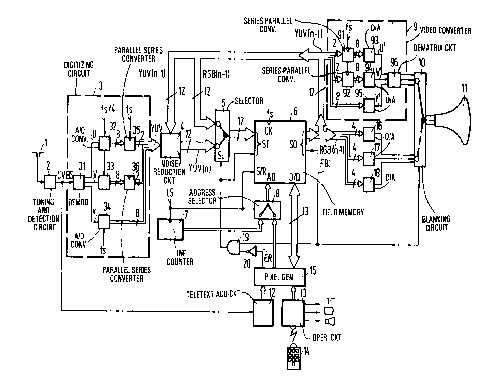
Fig. 1 shows diagrammatically an embodiment of a
television receiver according to the invention. The transmitter signals
received at an antenna 1 axe applied to a conventional 'tuning and
detection circuit 2. The composite video signal CV$S obtained therefrom
is applied, inter alia, to a digitising circuit 3. This circuit
comprises a demodulator 3'! for converting the composite video signal
into a luminance signal Y and 'two color difference signals U and V. The
luminance signal X is subsequently sampled at a so-called sample
frequency fs of, for example, 13.5 MHz, and quantised in eight bits in
an ~i/D converter 34. Identically, but at a quarter of the sample
frequency fs, 8-bit samples of the color difference signals U and V are
obtained from A/D converters 32 and 33, respectively. The samples of
these signals U and V are applied to parallel-series converters 35 and
36, respectively, for converting the 8-bit samples at a frequency fs/4
into four successive 2-bit parts at a frequency fs. Thus, 12-bit samples
YUV at a frequency of 13.5 MHz are available at the output of the
PHN 93.101 5 20.12.1989
digitising circuit 3. The composite video signal CVBS is digitised in
this way only during an active picture line period of approximately
53 psec. At said sample frequency of 13.5 MHz, 720 samples XUV are
generated far each picture line. A video field comprises 280 of these
picture lines with video information.
In this embodiment of the television receiver the
obtained samples YUV are applied to a first input of a noise reduction
circuit ~, a second input of which receives corresponding samples
YUV(n-1) of the previous video picture which has already been
displayed. The value of samples YUV(n) for the next video picture n to
be displayed is computed in the noise reduction circuit 4 from the
received samples YUV and the corresponding samples YUV(n-1) displayed in
the previous video gicture n-1. The relevant computation is irrelevant
for a good understanding of the invention and will not be further
described. The obtained samples YUV(n) are subsequently applied to a
first input of a selector 5 and to a field memory 6 via this selector.
In this respect it is tentatively assumed that selector 5 is in the
position shown in response to a selection signal having a logic value
"0" applied to an input Sb.
Tn the embodiment of the television receiver shown in
Fig. 1 field memory 6 is a so-called "dual port video RAM". Such a
memory is shown diagrammatically in Fig. 2 fox 1-bit wide data. It
comprises a random access memory section 61, generally known as DRAM,
which comprises 280 rows and 720 colu~ns. This DRAM has the conventional
connections such as an address input AD, inputs RAS and CAS for
identifying an applied address as a row or column address, a write input
WE and a combined data input and output D/Q. Moreover, an addressed row
is coupled by means of a bus 62 to a 720-bit shift register 63 which can
parallel be loaded or read and which is further provided
with a serial input SI, a serial output S0, and a clock input CK. The
memory also comprises a control circuit 64 having a mode input S/R for
selecting a serial or random access mode. In the random access mode the
memory is used in known manner as a DRAM. In that case a row and a
column address are successively applied to the address input AD in a so-
called random memory cycle and, dependent on the write input WE, a bit
is read or written via connection D/Q. In the serial access mode a row
and a column address are applied to address input AD in a so-called
PHN 13.101 6 20.12.1989
serial memory cycle. If the write input WE is not active, the entire
addressed row is transferred to shift register 63 in this mode. The 720
bits which are then available in the shift register are subsequently
applied successively to the output SO by means of a clock signal applied
to clock input CK, starting from the addressed column address. If the
write input WE is active, the 720 bits applied to the shift register 63
via input SI are transferred in a corresponding way to the addressed row
of the memory section 61.
In the field memory of the television receiver shown in
Fig. 1 thirteen of these memories are arranged in parallel for storing
the said 12-bit samples YUV(n) and a 13th bit which will further be
referred to as blanking bit. The blanking bit has the value of the
selection signal applied to the input SL of selector 5. It will be
tentatively assumed that it has the logic value "0", but it will
hereinafter be apparent when this is not the case. For storing the 720
samples YUV(n) of a picture line in the field memory, and for displaying
the 720 samples YUV(n-1), a picture line counter 7 applies the
corresponding picture line number via an address selector 8 to the
address input AD of the field memory upon the start of the relevant
picture line during a serial memory cycle intended for this purpose. As
a result the contents of the addressed memory row are transferred to the
shift register 63 (see Fig. 2). Whenever a clock pulse occurs at the
clock input CR, a sample YUV(n-1) becomes available at the serial data
output SO of the field memory 6. Simultaneously, a new sample YUV(n) is
stored in the shift register 63. At the end of the picture line the
contents of the shift register 63, which now comprise 720 new samples
YUV(n), are transferred to the addressed memory row and stored in this
row in a serial memory cycle for the same picture line number. It is to
be noted that for these operations address selector 8 is in the position
shown during said two serial memory cycli only. During the rest of a
picture line the address selector 8 is in the position not shown for
addressing, to be further described, by another source. To this end,
the address selector 8 is controlled, for example, by a line
synchronising signal LS. The line synchronising signal LS is also
applied to the mode input S/R for selecting the access mode.
The 12-bit samples YUV(n-1) obtained at the serial memory
output SO are applied to a video converter 9 for generating 'the three
PHN 13.101 7 20.12,1989
conventional red, green and blue (RGB) signals for display on a display
screen 11. To this end, video converter 9 comprises two series-parallel
converters 91 and 92 for converting four successive 2-bit parts at a
frequency fs into one full 8-bit U or V sample, respectively, at a
frequency fs/4, two D/A converters 93 and 94 fox abtaining analog color
difference signals U' and V', and a D/A converter 95 fox obtaining an
analog luminance signal Y'. Said series-parallel converters 91-92 and
D/A converters 93-95 have the complementary function of the previously
mentioned parallel-series converters 35-36 and A/D converters 32-34.
Furthermore, video canverter 9 comprises a dematxix circuit 96 for
converting the luminance signal Y' and calor difference signals U' and
V' into the RGB signals which can be displayed. These RGB signals are
applied via a blanking circuit 10 to the display screen 11 for
displaying the video picture in which the noise is now reduced.
In this embodiment the received composite video signal
CVBS from tuning and detection circuit 2 is also applied to a teletext
acquisition circuit 12. This circuit is adapted in known manner to
receive and store the picture information for a teletext picture to be
displayed. This teletext picture information generally comprises a
corresponding 8-bit code far each character to be displayed. The '
television receiver is also provided with an operating circuit 13. This
circuit is adapted to receive operating instructions which are generated
by the user by means of a (remote) control unit 14 and to control, in
response to these operating instructions, station tuning, picture
brightness, sound volume and the like. In Fig. 1 this is denoted by the
appropriate symbols. Particularly, operating circuit 13 is adapted to
generate the picture information for so-called On Screen Disglay
pictures. Such pictures may not only be simple texts, like channel
numbers, station names and the like, but also operating menus composed
of graphic images. For example, in operating circuit 13 the picture
information for an operating menu may comprise, for example, the
following picture description:
- draw a circle with a centre (360, 140) and a radius 15 in color 4080;
-- fill the circle with color 240;
- draw the letters "T" and "V" in color 4095 from position (348, 195).
This picture description defines a round green button encircled by a
yellow line and having a white inscription "TV" in the centre of the
PHN 13.101 8 20.12.1989
display screen.
The teletext picture information and the operating
picture information are applied far display to a pixel generator 15.
This generator is preferably in the form of a micxoprocessar and is
adapted to determine for each 'pixel to be displayed the display screen
position of this pixel, as well as a color code in, for example, 4 bits
of red, 4 bits of green and 4 bits of blue. Such a pixel generator is
known from Figs. 3 and 9 of "Comparative terminal realizations with
alpha-geometric coding" published in IEEE Transactions on Consumer
Electronics, Vol. CE-26, August 1980, pages 605-617. In the embodiment
shown in ~'ig. 1 of the television receiver use can be made of, for
example, a Graphics System Processor TMS 39010 of Texas Instruments. The
pixels of a teletext or operating picture to be displayed are generated
once and relatively slowly by the pixel generator 15, for example, not
faster than 1 pixel per psec. Moreover, the sequence of the pixels in
terms of their position on the display screen is arbitrary.
The 12-bit color codes generated by pixel generator 15
and further referred to as RGB pixels, are applied via a bidirectional
data bus to the random access data input and output D/Q of the field
memory 6. Moreover, the pixel generator generates the previously
mentioned blanking bit as the 13th bit. This blanking bit indicates by
means of a logic value "1" that the corresponding 12-bit code is an RGB
pixel to be distinguished from the previously mentioned 12-bit YUV
samples. 4Thile an RGB pixel is being applied to the field memory 6, the
pixel generator generates a memory address corresponding to the desired
position on the display screen 11, and applies it via address selector 8
to the address input AD of the field memory 6. As already stated, the
address selector 8 is substantially always in the position (not shown)
intended for this purpose. During a random memory cycle the RGB pixel
and the corresponding blanking bit are stored in the addressed memory
location. It is to be noted that the previously mentioned process of
serial writing and serial reading of the shift register 63 is not
disturbed.
Thus, both YUV samples corresponding to the video picture
to be displayed and RGB pixels corresponding to the teletext or
operating picture also to be displayed are stored in the field memory,
while for each memory element of the memory the type of the stored
~~~r~~W
PHN 13.101 9 20.12.1989
information is indicated by the blanking bit. Consequently, the signal
from the serial memory output SO comprises successive memory elements
which represent either samples YUV(n-1) or pixels RGB(n-1), as well as
blanking bits FBL corxespanding thereto.
The memory elements are not only applied to the video
converter 9 but also to three D/A converters 16-18 each of which
receives four bits of the memory element. If th~:se D/A converters
receive an RGB pixel, the conventional RGB signals are available at
their outputs for displaying this pixel in a color envisaged by the
pixel generator. Similarly as the RGB signals from video converter 9,
these RGB signals are applied to display screen 11 via blanking circuit
10. Furthermore, the blanking bit FBL corresponding to each memory
element is applied to blanking circuit 10, which bit blanks the video
picture obtained from YUV samples if an RGB pixel is available, and
blanks the teletext or operating picture if a YUV sample is available.
As a result it does not matter that YUV samples are also applied to the
D/A converters 16-18, and that RGB pixels are also applied to the video
converter 9.
The successive blanking bits FBL obtained from the field
memory are also applied to a first ingut of an AND gate 19. It will be
tentatively assumed that a logic value "1" is constantly applied to the
second input of this AND gate. During serial reading of memory elements
from field memory 6, the corresponding blanking bits FBL are applied via
the AND gate 19 to the input SL of selector 5 and to the 13th bit input
of the serial memory input ST of field memory 6. Consequently, each
blanking bit read from the field memory is stored again and in an
unchanged form. A blanking bit with the logic value "1" once generated
by pixel generator 15 is thus preserved. The other 12 bits applied to
memory input SI originate from the selector 5. If the blanking bit has
the logic value "0", this selector 5 selects a sample YUV(n) from noise
reduction circuit 4 for the purpose of storage, as has been described
hereinbefore. However, if the blanking bit has the logic value "1",
selector 5 selects a pixel RGB(n-1) applied to a second input thereof
from memory output SO in order to Store this pixel again. This is the
case when the memory element comprises an RGB pixel generated by the
pixel generator. Tn this way the pixels of a teletext or operating
picture stored once are protected from being overwritten by YUV samples.
PHN 13.101 10 20.12.1989
A teletext or operating picture thus displayed
simultaneously with a video picture can be erased, i.e. xeplaced bythe
video picture, in response to an erasing instruction. This exasing
instruction is generally applied to the pixel generator 15 by the
teletext acquisition circuit 12 (for example, upon receptian of a new
teletext page) or by the operating circuit 13 (for example, in response
to an operating instruction obtained from the remote control unit 19).
This generator addresses the pixels to be erased in the field memory 6
and stores the logic value "0" as 13th bit. If the corresponding memory
element is subsequently again written via the serial input SI, selector
5 no longer selects the pixel RGB(n-1) which is alxeady stored, but a
sample YUVfn) from noise reduction circuit ~ since the blanking
bit value has now been modified. However, it is not efficient to
erase relatively large operating pictures or even display screen-filling
telet~:ct pages in this way, because the individual addressing of a laxge
number of pixels by the relatively slow pixel generator 15 is time
consuming.
An efficient way of erasing a full teletext or operating
picture is provided by means of an erase signal ER which is applied by
the pixel generator 15 to the second input of the AND gate 19 via an
inverter 20. For the normal operating condition hitherto considered,
this erase signal ER has a constant logic value "0". However, in
response to an exasing instruction the. erase signal becomes active with
the logic value "1" during at least one video field period of 20 cosec.
As a result, AND gate 19 applies the logic value "0" to the 13th bit
input of the serial input SI of field memory 6, so that all blanking
bits in the field memory 6 obtain the logic value "0" and are thus
erased. Moreover, AND gate 19 applies the logic value "0" to the
selection input SL of selector 5, which thus simultaneously applies
a sample YUV(n) to field memory 6 for each memory element.
The erase signal ER can be generated in further known
manner. For example, the pixel generator 15, which is implemented as a
microprocessor, may be adapted by means of conventional pxogxam steps to
generate a pulse of 20 cosec at an output in response to the reception of
the erasing instruction from television acquisition circuit 12 or
operating circuit 13. It is to be noted that it is also possible to
generate the erase signal ER during a selected portion of a video field
PHN 13.101 11 20.12.1989
period, fox example, a portion corresponding to a rectangular box on the
display screen.
Another embodiment of the television receiver section
which is relevant to the invention is shown in Fig. 3. The noise
reduction circuit 4, field memory 6, address selector 8 and pixel
generator 15 shown in this Figure correspond to the circuits in Fig. 1
having the same reference numerals. In Fig. 3 field memory 6 comprises
conventional random access memories (RAMs). In this case the 13-bit wide
data input D and output Q are shown separately. In practice they may be
combined to one bidirectional data bus.
Now, 720 individual memory cycli are required for storing
720 successive samples YUV(n) from noise reduction circuit 4 in the
field memory 6 duzing the active picture line period. This is in
contrast to Fig. 1 in which only two memory cycli were necessary for
this purpose. DL.~ing each memory cycle a memory control circuit 21
applies a predetermined value of a selection signal S to a data selector
22 and to the address selector 8, Which in response thereto are in the
positions shown. The field memory is now addressed by memory control
circuit 21 via address selector 8 and receives a sample YUV(n) from
noise reduction circuit 4 via a first input of data selector 22, while a
logic "0" is applied as the 13th bit. In Fig. 3 each one of the 720
memory cycli for storing YUV samples is a so-called "read-modify-write"
cycle comprising two time intervals. In the first time interval the
addressed memory element is read for display and for its supply to the
noise reduction circuit 4. Moreover, the blanking bit FBL corresponding
to the memory element obtained is applied to a first input of an AND
gate 24,after inversion by an inverter 23. In the second time interval
memory control circuit 21 generates a first write signal W1 with logic
value "1" and applies it to a second input of this AND gate 24. If the
blanking bit FBL now has the logic value "0" which as previously stated
means that the memory element which has been read comprises a YUV
sample, the output of AND gate 24 acquires a logic value "1" in
response thereto. This output is connected to a first input of an OR
gate 25 whose output signal is applied to a write input WF of the field
memory 6. The addressed memory element thereby acquires a new value
YUV(n) from the noise reduction circuit, while a logic "0" is stored as
13th bit. However, if the blanking bit FBL has the logic value "1",
PHN 13.101 12 20.12.1989
which means that the memory element comprises an RGB pixel, a logic "0"
is applied to the first input of AND gate 24 via inverter 23. The write
signal W1 applied to the second input of AND gate 24 is now suppressed
for the addressed memory element so that there is no storage of a YUV
sample and the RGB pixel, which has already been stared, is preserved.
If memory control circuit 21 does not apply the value of
selection signal S for storing YUV samples to data selector 22 and
address selector B, these two selectors are in the other positions. In
these positions, which are not shown, the field memory 6 is connected to
the pixel generator 15 far storing RGB pixels and blanking bits
corresponding thereto. Write input WE of the field memory 6 is activated
in this case by a second write signal W2 which is generated by 'the pixel
generator and applied by this generator to the memory via a second input
of OR gate 25.
Furthermore, the television receiver shown in Fig. 3 is
adapted to generate the erase signal ER. For erasing a teletext or
opexating picture, this erase signal with the logic value "1" is applied
to a first input of an AND gate 26 which receives the write signal W1 at
a second input. The output of this AND gate 26 is connected to a third
input of an OR gate 25, so that the write input WE of the field memory
is activated for each applied sample YUV(n) and the corresponding 13th
bit with logic value "0", independent of the value of the blanking bit
FBL received via AND gate 24.
In the television receiver shown in Fig. 3 the access to
field memory 6 by pixel generator 15 is limited to the portion of a
television field period in which no YUV samples are generated. To this
end, the selection signal S corresponds, for example, to the horizontal
and vertical flyback period of the video signal. In that case, only a
small portion of the field period is available for storing RGB pixels.
As a result, the rate at which a teletext or operating picture is
generated by the pixel generator 15 is considexably slowed down.
However, it is possible to alternate, within the active picture line
period, one or more read-modify-write cycli for storing YUV samples with
a memory cycle for storing RGB pixels. The selection signal S is applied
to pixel genexator 15 so as to inform it of the position taken up by
data selector 22 and address selector 8.
For the sake of completeness it is to be noted that it is
PHN 13.101 13 20.12.1989
useful in the shown embodiments of the television receiver according to
the invention to compose teletext and operating pictures in fields of
tour successive RGB pixels. Tn fact, if this is not the case, and if,
for example, one RGH pixel and three YUV samples are stored in four
successive memory elements of the field memory 6, the video converter 9
generates one full 8-bit U sample and one full 8-bit V sample for these
four memory elements in the manner described hexeinbefore. The
corresponding values of the color difference signals U' and V' from D/A
converters 93 and 94 (see Fig. 1) are, however, dependent on the stored
RGB pixel and they are no longer related to the video signal to be
displayed originally. Thus, color errors in the video picture are
produced at the edges of an individual RGB pixel. This is prevented by
storing four RGB pixels. In this connection it is also useful to store
not more than one blanking bit for four successive memory elements in
the field memory 6. A possible embad=meat of the field memory 6 shown in ,
Fig. 3, with which this is achieved, is shown in Fig. 4. In this Fig. 4
the field memory 6 is split up into a first 12-bit wide memory 65 for
storing YUV samples ox RGB pixels, a separate second memory 66 for
storing blanking bits and an address converter 67. Memory 65 is split up
into 280 rows and 720 columns in the manner described hereinbefore.
Memory 66 is split up into 280 rows and only 180 columns. The address
converter 67 is adapted to perform such a conversion of the applied
address AD that four consecutive columns in memory 65 correspond to one
column in memory 66, for example, by ignoring the two least significant
bits of the applied address. This also leads to a considerable economy
in the memory required for storing blanking bits.
The occurrence of the afore-mentioned color errors in the
video picture can also be prevented by always storing the 2-bit U parts
and 2-bit V parts of a sample YUV(n) (see Fig. 1) in all memory elements
of the field memory 6, independent of the corresponding blanking bit.
The other 8 bits of the memory element then either comprise the 8-bit Y
sample or the RGB pixel. The color difference signals U' and V' are now
no longer disturbed. An RGB pixel now comprises 8 bats so that the
number of color gradations in a teletext or operating picture is limited
to 256.
Finally it is to be noted that the pixel generator 15 in
the television receiver according to the invention may alternatively be
~ ~- r~~ '~ ~ ~:
PHN 13.101 14 20.12.1989
adapted to generate a teletext or operating picture comprising YUV
samples instead of RGH pixels. In that case the three D/A converters 16-
18 and blanking circuit 10 are omitted in Fig. 1. A teletext or
operating picture obtained in this way has considerably less definition
8 due to the smaller bandwidth of the color difference signals. The
television receiver, may alternatively be adapted to store the video
signal in the form of RGH values, which will then often comprise 24
bits. However, the blanking signal remains necessary for identifying
memory elements corresponding to the video picture and memory elements
corresponding to the teletext or operating picture.