Note: Descriptions are shown in the official language in which they were submitted.
2~ 7 ~2
O LOW HEIGHT CHIP CARRIER SOCXET
This invention relates to sockets for integrated
circuit chip carriers having flexible leads and, more
particularly to a low height chip carrier socket for
electrically connecting such a carrier to conductors
on a substrate.
There is a packaging technology for integrated
circuit chips generally known in the industry as
"Tape Pak". This technology involves attaching the
chip to a lead frame in the usual manner, including
wire boncled interconnections, and then molding a
plastic carrier body which completely surrounds the
chip with the leads of the lead frame extending
outwardly from the sides of the body. A
rectangularly shaped ring of plastic is also molded
to completely surround but be spaced from the sides
of the carrier body in the plane of the leads, the
leads extending through the sides of the ring. Such
a structure, shown in Figures 1 and lA, includes a
chip carrier 10 having a plurality of leads 12
extending outwardly from the four sides of the
carrier 10 and through the sides of a ring 14. The
lead frame 16 and the leads 12 are stamped or etched
from a thin sheet of copper or other suitable
material in a manner that is well known in the
industry. The thickness of the material is usually
14678 CA
2 ~
--2--
about 0O005 inches and the width of the leads is
typically o.o1o inches or less. Typically, several
lead frames 16 are formed end to end in a strip, as
shown in Figure 1, so that several IC carrier
packages can be formed simultaneously. After molding
they are separated by sheariny, for example, along
the line 18.
The outer portions 20 of the lead frame 16 are
then sheared off leaving the individual extensions 22
of tha leads 12 projecting from the ring 14. These
projections are then bent about 90 degrees against
the outer edge of the ring and are available for
contacting. The device is then places into a socket
which makes contact with each lead extension 22 for
purposes of testing the integra~ted circuit and for
exercising the integrated circuit at a high
temperature in order to accelerate ~anifestations of
possible failure modes of the clevice~ more commonly
known in the industry as "burn-in".
After testing and burn-in, the ring 14 is
removed by severing the individual lead 12 close to
the ring 14. The leads 12 may then be formed in
accordance with industry accepted specifications
developed by JCII Standards Committee (JEDEC~ prior
to soldering ox socketing. The complex trimming and
forming operations required by the JEDEC
14678 CA
2 ~! ~ r~
Specifications are expensive to perorm and rPsult in
relatively low yield. Further, some of the
dimensions are specified with very liberal tolerances
which adds to the difficulty of providing a highly
reliable socket. The difficulty is in handling and
connecting to such extremely fragile leads.
What is needed is a greatly simplified procedure
and apparatus for sockating such devices while
providing highly reliable socket interconnections,
and at low haight.
The foragoing and additional objects are
attained in accordance with the principles of this
invention by providing a low height chip carrier
socket for electrically connecting leads on the chip
carrier to respective pads on a mounting surface.
The leads are spaced apart and project from a
peripheral edge of the chip carrier. The socket
includes a base having a chip carrier receiving
cavity and a plurality of contacts in the base for
elsctrically connecting each lead to a respective
printed circuit board pad. Each contact includes a
contactin~ portion and an opposed backup portion,
both o~ which project from a common bight portion.
Means is provided for positioning and aligning each
contact with a respective lead so that each lead is
adjacent its respective contacting portion. Locking
14678 CA
~ ~ 2 t~
means is provided for wedging between each lead and
its respective backup portion so that the lead is
urged into pressing electrical contact with the
contact portion.
The advantages hereof will become apparent from
the exemplary teachings hereinafter when read in
conjunction with the following drawings in which:
FIGURE 1 is a plan view of a Tape-Pak structure
showing an inte~ral circuit chip carrier;
FIGURE lA is a sectional view taken along the
lines lA-lA of Figure l;
FIGURE 2 is an isometric view showing the chip
carrier of Figure 1 in relakion to the socket of the
present invention;
FIGURE 3 is a side view of the assembled socket
of Figure 2;
FIGU~E 4 is a partial s~ctional view showing the
chip carrier and the components o~ the socket prior
to insertion and assembly;
FIGURE 5 is a view similar to that of Figure 4
showing the chip carrier inserted into the lower half
of the socket; and
FIGURE 6 is a view similar to that of Figure 5
showing the chip carrier and socket completely
assembled.
14678 CA
7 i ~ ~
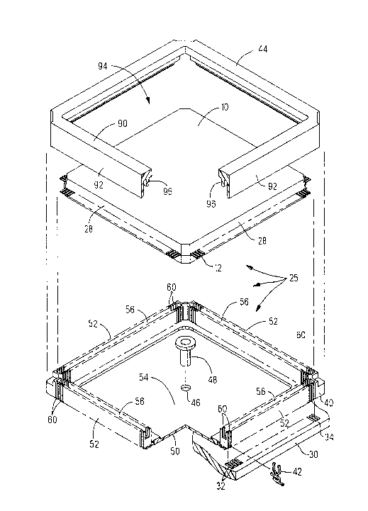
There is shown in Figures 2 and 3 an integrated
circuit chip carrier socket 25 for socketing the chip
carrier 10. The chip carrier 10, in the present
example, has relatively short leads 12 projecting
outwardly from the edges 28. The leads 12 are spaced
apart and are substantially flat and straight after
being severed from the ring 14 shown in figure 1. A
substrate or printed circuit board (PCB) 30 is shown
having conductive pads 32 arranged in a rectangular
pattern on a major surface 3~ of the PCB 30. The
purpose of the socket 25, of the present invention,
is to interconnect the lead 12 with respective ones
of the pads 32.
The socket 25 is composed of a body 40, a
plurality of contacts 42, and a cover 44. A central
hole 46 is provided through the body 40 throu~h which
a rivet or eyelet 48 is inserted for fastening the
soc~et 25 to the PCB 30 prior to soldering. The body
40 includes a bottom 50 and four upstanding walls 52
which form a chip sarrier receiving cavity 54
therewithin. The bottom 50 and walls 52 are of
molded plastic unitary construction. A longitudinal
groove 56 is formed in each wall 52 as shown in
Figures 2 and 4, for a purpose that will be discussed
below. A plurality of lateral slots 60 are formed
through each wall 52 as shown in Figure 2 and are
14678 C~
,~
~ ~ 7~,~f3
dimensioned to loosaly receive the contact 42
therein, as best seen in Figure 4. The slots 60,
which may be as little as o.o1o of an inch wide to
0.5mm or more, depending on the width of the leads
12, are arranged to leave a bottom web 62 which
interconnects the bottom 50 and the remaining
portions of the wall 52 for addPd strength. The
slots 60 are spaced so that when the socket 25 is
properly aligned and attached to the PCB 34 by means
of the rivet 48, each slot 60 is directly over a
respective one of the pads 32.
The contact 42, as best seen in Figure 4 is made
of a single piece of flat sheet metal, such as copper
alloy for example, having a thickness that is about
the same as the width of the leads 12, about 0.010
inch in the present example. The contact 42 includes
a U-shaped base 64 which is siz~ed to closely slip
over the web 62. A small protrusion 66 is formed on
one of the inner surfaces of ~he U-shaped base 64 in
a position to engage a hole 68 disposed in the web 62
so that as the contact 42 is inserted into the slot
60 in the direction of the arrow 70 of Figure 2, the
U-shaped base snaps firmly into place about the web.
A terminal 72 extends from one side of the U-shaped
base 64 and into engagement with the pad 32 as best
seen in Figure 4. A pair of openin~s 74 are provided
14678 CA
~ J7
in the pad engaging surface of the terminal 72 to
provide space for solder to accumulate when the
terminal is soldered to the pad. The contact 42
also includes a tuning fork portion projecting
upwardly from the base 64 into the slot 60 which
includes a contacting portion 80 and an opposed
backup portion 82. The contacting portion 80 and
backup portion 82 both project from a common bight 84
which is attached to the U-shaped base 64 through a
pivotal zone 86. The pivotal zone 86 is a relatively
narrow section which permits a small amount of
pivotal movement of the tuning fork in the directions
of the arrows B as shown in Figure 4. The purpose of
this pivotal zone 86 will be set forth below. The
terminal 72 extends outwardly Xrom the wall 52 to
permit reflow soldering by a reflow heating tool,
focused infrared radiation, hot gas ~low, or other
such reflow techniques. This also permits optical
inspection of the soldered terminal. As set forth
above, the openings 74 in the pad engaging surface of
the terminal 72 create a condition that is conducive
to the formation of solder fillets thereby enabling
the soldered interface to be stronger than it would
otherwise be. Those skilled in the art will
appreciate that the terminal 72, instead of b~ing
arranged for surface soldering, could be arranged to
14678 CA
'
2 ~
extend downwardly through a plated through hole~ or
the like, formed in the PCB 30 in a manner that is
well known in the industry. In the present example
where the terminals 72 area surface mounted, the body
40, containing the contacts 4~ in the slots 60, is
accurately positioned on the surface 34 of the PCB 30
so that the terminals 72 are in alignment with their
respective pads 32. The rivet or eyelet 48 is then
inserted into the hole 46 and through a hole in the
PCB 30. The rivet or eyelet 48 is peened to provide
a downward force on the bottom 50 that slightly
deflects the center of the bottom 50 toward the
surface 34 of the PCB 30. This downward deflection
of the bottom 50 tends to cause all of the terminals
72 to come into engaging contact with their
respective pads 32, or at least to come very close
thereto. In this way, minor variations in the
flatness of the PCB 30 can be tolerated.
The cover 44, as best seen in Figures 2 and 4,
comprises a rectangularly shaped top 90 being of the
approximate shape and dimensions of the body 40 and
includes a peripheral shroud 92 projecting downwardly
from the four sides of the top 90. The top 90 is
~imensioned so that the peripheral shroud 92 will
slip over the body 40 with minimum clearance between
the wall 52 and the shroud 92. The top 90 has a
14678 CA
g~
clearance opening 94 so that, when assembled to the
body 40, as shown in Figure 6, the carrier body 10
may project part way into the opening g4. The top 90
includes a locking member g6 which proiects
downwardly, as viewed in Figure 4, and is spaced from
the shroud 92 so that it will be in approximate
centering alignment with the slot 56 that runs for
substantially the length of the slot. Tharefor, when
the top 90, chip carrier 10, and base 40 are
assembled as shown in Figure 6, the locking member 96
is positioned within its respective slot 56.
Prior to inserting a chip carrier 10 into the
socket 25, the leads 12 are sheared to a specific
length leaving them flat and straight. The length of
the sheared leads is very short, approximately 1.5mm
in the present example. The carrier 10 iæ then
placed in the body 40, as best seen in Figure 5, so
that all of the leads 12 are loosely positioned
within their respective slots 60. The cavity 54 and
slots 60 are dimensioned so that the cavity 54
loosely aligns the carrier 10 as the carrier enters
the cavity thereby aligning the leads 12 with the
slots 60. Note that no force is required in placing
the carrier into the cavity 54. As seen in Figure 5,
the leads 12 rest on top of the contacting portionæ
80 and extend toward but are short of the backup
14678 CA
~7 ~
--10--
portions 82. Note also that the contacting portion
80 and backup portion 82 are substantially centered
with the groove 56 which is to provide clearance for
the locking member 96.
With the chip carrier lO in position within the
base 40, the cover 44 is lowered toward the base 44
as indicated by the arrow in Figure 5. The inner
surface 100 of the shroud 92 engag~s the walls 52
thereby aligning the locking members 96 with the
grooves 56. As the cover 44 is further lowered the
rounded ends 102 of the locking members 96 engage the
leads 12 and begins to deflect them downwardly,
bending them about the contacting portions 80 of
their respective contacts 42. Note that the rounded
end 102 is a camming surface which may take the form
of an angled surface or other suitable shape. This
~ownward mo~ion continues until the rounded ends 102
engage the bottoms 104 of the slots 56. At this
point the leads 12 have been benk about 90 degrees
downwardly, as viewed in Figure 6, and are pressad
against and into electrical contact with their
respective contacting portions 80. This pressing of
the lead 12 against its con~acting portion 80 is
ef~ected by means of energy stored in the expanded
tuning fork which acts in a direction lateral to the
bent lead 12.
1~678 C~
2 ~ 12
The distance batween the contacting and backup
portions 80 and 82 is less than the combined
thickness of the locking number 96 and the lead 12 so
that the tuning fork is caused to expand when the
cover 44 is assembled as described above. This
assures a contact force of about 14 grams between the
contacting portion 80 and the lead 12. It is
understood that the locking members 96 may not be
perfectly straight or all of the contacts 42 in
perfect alignment therewith. To accommodate such a
condition, the contact will align its~lf with the
locking member 96 as the end 102 bagins to bend the
lead 12 and engages the backup portion 82, by
pivoting in the appropriate direction about the
pivotal zone 86 as described previously.
Notwith~tanding misalignment of the locking member 96
or slight warping of the body 40, the tuning fork
will pivot about the pivotal zone 86 to properly
position itself so that the lead 12 is wedged between
the contacting member 80 and the locking member 96.
It should be noted that as the rounded end 102 of the
locking member 96 begins to bend the lead 12 and
engage the backup member 8~, a wedging action takes
place. This wedging action expands the tuning fork,
and continues until the rounded end 102 has
completely enter~d and the lead 12 and backup portion
14678 CA
7 ~
-12-
engage the relatively straight and parallel sides of
the locking member 96. Further insertion toward the
bottom 104 of the groove 56 will cause no further
expansion of the tuning fork thereby keeping the
contact ~orc~ within a predictable range of between
about 150 grams to about 220 grams.
An important advantage of the present invention
is the low height which results from this noval
structure. This low height socket is useful in
compact machines such as small lap top computers,
ultra thin wall hung televisions and many other
applications having very limited space. Another
important advantage of the present invention is the
relatively short electrical path provided by the
socket. The reduction of electrical length enables
higher speed switching and provides substantial other
related advantages. Further, the compact structure
of the present invention utilizes a smaller amount of
material than would otherwise be required, resulting
in lower production costs. Another important
advantage of the present invention is that a separate
step to form the leads in unnecessary resulting in
lower manufacturing cost and less chance of damaging
the fragile leads. Additionally, since the contact
force is supplied by energy stored in the tuning fork
structure which acts literally with respect to the
14678 CA
cl
leads of the device, no hold down structure is needed
as is required by prior art sockets.
14678 CA