Note: Descriptions are shown in the official language in which they were submitted.
2027'~0
AD-5Q34-A
TITL~
ELECTRONICS PROTECTIVE PACKAGING FILM
BACKGROUND_OF THE INVENTIO~
This invention relates to novel composites
useful for machine packaging electrostatic sensitive
electronic components or assemblies to protect them
from damages due to electrostatic discharge, electro-
static field force, radio-freguency interference,
moisture, and corrosive gases.
Functional failures or manufacturability
impairments of modern electronics components or
assemblies are often traceable to damage due to
electrostatic discharge, electrostatic field force,
radio frequency interference, moisture, corrosive
gases, and machine oil they may experience during
shipping and stora~e. The problem has increased in
severity in recent years and will continue to worsen
because of the increased miniaturization and speed of
devices and systems, like VLSI (Very Large Scale
Integration) chips, the impact of new automated
manufacturing processes such as high heat and chemi-
cal, e~g., oil, solvents, etc., exposure in a surface
mount assembly line, and the increased demands for
higher reliability.
Packaging materials have been developed for
electrostatic discharge protection. U.S. Patent
3,572,499, for example, discloses a composite
laminated material in sheet form comprising a layer of
thin sheet metal, typically aluminum foil, a layer of
20~30
protective material secured to one face of the metal
layer (to form the outside of a package or container)
and an exposed layer of an electrically conductivë,
synthetic organic polymeric plastic material (to form
the interior surface of the pacXage or container).
The protective material is preferably paper or fabric,
and the conductive plastic material is preferably
polyethylene filled with a non metallic filler such as
carbon.
U.S. Patents 4,156,751 and 4,154,344
disclose a flexikle sheet material for forming an
envelope used to enclose and protect electronic
components from electrostatic charges~ The envelope
includes a polymeric sheet, an antistatic material
l~ disposed at an inner surface, and a conductive layer
disposed on the outer surface. The inner, antistatic
layer acts as a humectant surface to collect water to
reduce friction and minimize static charges. The
external (metallized) layer has light transmissivity
of at least 25 % (optical density of at the most 0.6).
U.S. 4,424,900 discloses an anti-static
package composed of a multi-ply flexible film. The
inner ply is an antistatic material and the outer ply
- is an electrically insulating material. A conductive
metallic ply is sandwiched between the inner and outer
ply. The antistatic ply is an antistatic polyolefin
material; the metallic ply is a thin sputtered layer
of, e.y., stainless steel, preferably having a light
transmission in excess of 70% ~optical density of at
most 0.15).
U.S. 4,699,830 discloses a laminated sheet
material which can be used to form packages for
electrically sensitive components. The laminated
sheet includes an antistatic layer, a first and a
second conductive metal layer, and a carrier film
layer. The antistatic layer can be a polyolefin-based
-- 2 --
20~7~3~
3 --
material. The metal layers are vacuum deposited
layers, preferably thin enough to permit light trans-
mission in combination of 15-70% (o.d. 0.15-0.82).
Corresponding Canadian Patent Application
Serial No. 611,663, filed September 15, 1989, describes
an electroconductive powd~r composition comprising a
amorphous silica particles which are uniquely
associated with a two-dimensional network of
antimony-containing tin oxide crystallites. This
powder can be incorporated as a component within a
polymeric carrier matrix which can take the form of a
paint film, fiber, or a variety of shaped articles.
Many of the prior art packages or films
employ antistatic agents which are moisture dependent
or which consist of carbon particles, but which can
also contaminate sensitive electronic components.
Furthermore, such packages do not always provide the
most satisfactory barrier properties against moisture
or other contaminants. Many such packages, in
addition, can be bulky, stiff, or too thick to be
readily used in automated packaging machinery. ~he
present invention provides new packaging materials for
protective packaging of electrostatic, radio frequency
interference, and mois~ure sensitive electronic
components or assemblies, readily usable in automated
form, fill, and seal packaying machines, thus
overcoming many of the deficiencies of prior art
materials.
3~ SUMMARY OF_THE INVENTION
The present ~nvention provides a flexible
static charge-dissipating structure comprising:
(a) a substrate film;
(b) a coating of at least one layer selected
~rom a heat sealable thermoplastic matrix or latex on
at least one surface of said substrate film: and
- 3 -
: '
-' .
20~7~3~
, - 4 -
(c) particles of a silica-containing
material, surface coated with a two-dimensional
network of antimony-containing tin oxide crystallites
in which the antimony content ranges from about l to
5 about 30 percent by weight of the tin oxide, said
particles being dispersed in at least one layer of
said matrix and being present in sufficient quantity
to provide a surface resistivity of less than about
1012 ohms per square.
The flexible structure of the invention
exhibits a high heat seal strength of up to at least
about 626 grams/cm and oil resistance which can meet
or exceed military specifications.
The invention also provides a similar
structure further comprising a thin, flexible layer of
metal of sufficient thickness to provide
electromagnetic interference shielding in the
frequency range of 0.1 to 10.0 gigahertz of at least
about 25 db, as well as improved barrier properties.
BRIEF DESC~IPTION OF THE FIGURES
Figure 1 illustrates one preferred
embodiment of the structure of the present invention.
Figure 2 shows a package or pouch prepared
from the structure of the present invention.
Figure 3 shows an alternative package of the
present invention.
DETAILED DESCRIPTION O~ HE INVENTION
The substrate material of this invention is
a polymeric film which has sufficient puncture
resistance to endure the rigors of modern shipping and
handling. Yet for many applications the film should
not be so thick or stiff that it cannot be readily
formed into a flexible package or bag using
conventional packaging equipment. In addition, the
, - 4 -
.
20~43U
- 5 -
film will preferably have sufficient dimensional
stability to endure a vacuum metallization process
(commonly involving temperatures of about 100-C)
without shrinking or otherwise distorting.
Suitable substrate films include those made
of polyesters such as polyethylene terephthalate
(PET), polymethylpentene, polyarylate, polypropylene,
nylon, polycarbonate, cellophane, polyetherimide,
polyimide, and the like. A preferred substrate is
biaxially oriented polyethylene terephthalate. Such a
film is preferably at least about 10 micrometers but
less than about 100 micrometers thick. Particularly
suitable are such films having a thickness of from
about 20 to about 25 micrometers. For improved heat
sealability and oil resistance the preferred film
substrate is oriented linear low-density polyethyiene,
such as, for example, Sclair~-SC, available from
Du Pont (Canada).
At least one surface of the substrate film
is coated with at least one layer of a heat sealable
thermoplastic material or latex. This material serves
to provide heat sealability if desired for, e.g.,
package formation and also serves as a matrix to carry
selected electroconductive particles, described below.
Suitable heat sealable thermoplastic materials are
known in the art: particularly suitable resins include
polyesters selected from the group consisting of
copolymers of ethylene glycol, terephthalic acid, and
azelaic acid; copolymers of ethylene glycol,
terephthalic acid, and isophthalic acid; and mixtures
o~ such copolymers. The heat sealable thermoplastic
material can be a composition of such copolymers with
minor amounts of conventional additives including
block or slip agents such as stearic acid, stearamide,
or erucamide and fillers such as magnesium silicate.
.
206~7~3~
At least one layer of the heat sealable
thermoplastic material serves as a matrix to carry
~elected electroconductive particles. Such particles
should be contained in a surface or near-surface layer
of material so that they can sPrve to impart static
dissipative properties to the film structure. The
electroconductive particles preferred for the present
invention and their preparation are described in Canadian
Patent Application Serial No. 611,663- The electrocon
ductive particles are micron-sized particle~ of a
silica-containing material, surface coated with a
two-dimensional network of antimony-containing tin
oxide crystallites in which the antimony content
ranges from about 1 to about 30 percent by weight. By
"micron-sizedn it is meant that the average diameter
or greatest dimension of the particles is on the order
of about 0.2 to about 20 microns, preferably about 1
to about 10 microns.
The silica-containing material is, in
general, a material having an extensive co-valent
network involving SiO4 tetrahedra, thus offering the
potential for surface hydroxyl formation. The
preferred material is amorphous silica. The
silica-containing material can be in practically any
shape but is preferably in the form of platelets or
hollow shells. Platelets of silica-containing
material can be formed by coating the material on
flake-shaped particles such as mica. Hollow shells
can be formed by coating a finely divided solid core
material with active silica and then removing the core
material without unduly disturbing the silica coating.
In either case, the silica coating or shell should be
relatively thin, less than about-250 nm and preferably
- 6 -
.
20'~7 ~3~
in the range of about 5 to about 20 nm. Alternative-
ly, the silica coating can be formed on permanent core
particles of, e.g., Tio2 or clay.
The silica-containing material is coated
with a substantially two-dimensional network of
densely packed antimony-containing tin oxide
crystallites. The layer of such crystallites is
typically about 5 to 20 nm thick, but covers the
surface of a particle with major dimensions that are
typically ten to ten thousand times as large as the
thickness of the tin oxide layer, and thus is
substantially two dimensional. The tin oxide
crystallites contain about 1 to 30 percent by weight
antimony, preferably about 10 percent by weight.
The electroconductive particles tECP) are
dispersed in the matrix polymer at such a
concentration that a certain amount of electrical
conductivity is imparted to the matrix polymer and
thus to the film structure. In order to obtain a
coated film with a surface resistivity of about 10l2
ohms/square or less, the concentration of ~CP in the
matrix should be at least about 25%. For many
applications, such as packaging films suitable for
protecting electronic components from stat~ic
discharge, a surface resistivity of at least lO5
ohms/square but less than 10l2 ohms/square is desired;
in such cases the concentration o~ ECP should be about
25 to about 55% by weight, or more preferably about 30
to about 40%.
Of course, the resistivity of the film
surface will depend in part on the thickness of the
matrix layer containing the ECP. Very thin layers
will exhibit increased resistivity, and vice versa.
While surface coating of about 1 to about 25 g/m2 (in
terms of combined matrix and ECP) may be suitable,
preferably the coating will be present at about ~ to
; - 7 -
,: 1 . ,;
2~4~
- 8 -
about 12-13 g/m2. The physical thickness of such
coatings is typically several micrometers.
Such coatings are typically applied by a
solution coating process, wherein the matrix polymer
is dissolved in a suitable solvent and the ECP is
dispersed therein. A coating of solution is appliad
by spraying, dipping, or coating with a doctor knife,
followed by removal of the solvent, e.g., by a hot air
or radiant dryer.
A preferred em~odiment of the present
invention comprises a film structure which
additionally comprises a thin, flexible layer of
- metal, preferably located as an interior layer of a
multilayer structure. This additional layer provides
electromagnetic interference (EMI) shieldinq. EMI
shielding is often desired in packaging for sensitive
electronic components, and can be provided by a vacuum
deposited layer of metal, deposited on the substrate
film by well-known techniques. Alternatively, EMI can
be provided with a~heat sealable/metal foil structure
instead of a metallized film, such as, for example,
with a Surlyn~foil substrate. In either case, the
metal is not particularly limited, although metals
which are relatively unreactive to air and moisture
are preferred. Most specially preferred is aluminum.
A vacuum deposited layer of aluminum of sufficient
thickness to exhibit surface resistivity of 40
ohms/square or leæs, and preferably 10 ohms~square or
less, provides useful shielding properties. These
levels correspond to optical densities of about 0.5
and 0.9, respectively. The upper limit in terms of
amount of metallization depends on economic factors
and the necessity of maintaining a flexible film
structure for many packaging applications.
EMI shielding can be e~aluated in terms of
, reduction of intensity of an electromagnetic signal of
-- 8 --
20~3~
_ 9 _
1 to 10 GHz upon passing through a test film. For
many demanding applications, a reduction of at least
25 decibels (db) is desired.
An additional benefit derived from the use
of a thin layer of metal in the composition is a
marked improvement in barrier properties to such
substances as water, oxygen, or corrosive materials.
Particularly demanding applications may re~uire water
vapor transmission rates of at most 1 g/m2-day or
better. These stringent barrier requirements can be
met or exceeded by laminating two layers of metailized
together so that the layers of metal are joined face
to face. Such an arrangement minimizes the problems
of penetration of contaminants through pinholes that
may be present in a single metallized layer.
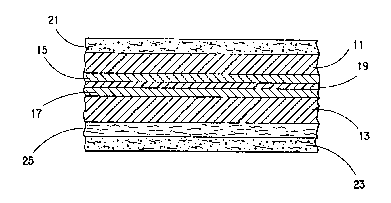
A highly preferred structure, therefore, is
a face-to-face laminate of two metallized substrate
~ilms, with coatings of heat sealable thermoplastic
material or latex containing ECP on at least one, and
preferably both, of the outer surfaces. Such a
structure is shown diagrammatically in Figure 1.
Substrate films 11 and 13 each support a layer of
vacuum metallized aluminum, 15 and 17. The films are
joined using a conventional adhesive layer 19. The
two outermost layers, 21 and 23, are heat sealable
matrix resin compositions in which ECP is dispersed.
Layer 25 is an optional underlying layer of heat
sealable resin matrix compositions substantially free
o~ ~CP; a corresponding layer (not shown) may
optionally also be present underlying outer layer 21.
The additional heat sealable layer, when present,
improves the strength of heat seals when the film
structure is formed into a pac~age.
The preferred structures of the present
invention are strong and flexible, have excellent EMI
shielding and barrier properties. They also have
_ g _
- 20~ ~ 430
-- 10 --
excellent static dissipative properties, as measured
by the rate of decay of a static charge (normally less
than 0.5 seconds, in comparison with a desired goal of
2 seconds). This static dissipative property is
virtually insensitive to moisture, in contrast to the
behavior of many conventional systems which are much
less effactive under dry conditions. Moisture
insensitivity is important for packaging of electronic
components which may themselves require both
protection from static discharge and a dry storage
environment.
The invention further comprises protective
packages prepared from films and laminated structures
of the present invention. A simple pacXage or po~ch
is shown in Figure 2. The pouch or bag 31 is formed
from a front leaf 33 and a back leaf 35 joined along
the edges by a heat seal 37 or other means. The front
and back leaves can be made from different pieces of
coated structure, or they can result from folding a
single sheet over on itself along a crease 39 (in
which case a seal at that location is not needed).
When an item is inserted in the pouch, the open end 40
can be similarly sealed. While a simple pouch-like
structure as illustrated is preferred for simplicity,
other packages can equally well be formed, such as
gussetted bags, and so on. In particular, Figure 3
shows a box 41 made of cardboard or a similar
structural material 43. The inner surfaces 45 of the
cardboard is lined or laminated with the film or
laminated structures of the present invention.
Packages such as those illustrated provide
protection to packaged items from static discharge,
even when the interior of the package is very dry.
Furthermore, the presence of one or more layers o~
vacuum deposited metal serves to keep ambient humidity
from penetrating into a sealed package, as well as
-- 10 --
2t; ~43~
providing EMI shielding. Such packages can be used
for shipping and storing electronic components such as
semiconductor wafers, surface mount and through-hole
components, integrated circuit chips, subassemblies,
finished assemblies, populated and unpopulated printed
circuit boards, and larger electr~nic components such
as personal computer keyboards. Other uses include
packaging of medical and surgical products and general
use for packaging in explosive environments.
Measurement Procedures
The following measurement procedures are
used for the Examples:
15 MEASUREMENT PROCEDURE
Surface Resistivity ASTM D-257
Puncture Resistance Federal Test Method 101-2065
EMI-Shielding and Military specification
Oil Resistance
~ MIL-B-81705C, January 25,
1989, obtainable from
Naval Air Engineering Center,
Lakehurst, NJ 08733-5100,
unless otherwise indicated.
Decay Time Federal Test Method 101-4046
Water Vapor
Transmission Rate ASTM F-1249 (38.7-C, 90% RH,
(WVTR) using a ~Permatran-W~ from
Modern Control, Inc.) ,~
30 Optical Density AIMCAL ~P-101
Light Transmission ASTM D1746-40
ExamPles 1-9 and Comparative Examples Çl-C4
The following Examples and Comparative
Examples illustrate the effective amounts of
electroconductive particles in thermoplastic matrix
.
. . . .
~0~7~3~
- 12 -
coating which provide static dissipative film surfaces
at both dry and ambient humidity conditions.
The electroconductive particles are
antimony-containing tin oxide-coated fine silica
hollow shells as disclosed in corresponding Canadian ,
Patent Application S~rial No. 611, 663 .
In a 189 L glass lined kettle, agitated with
an anchor type 0.46 m impeller turning at so rpm, 76 L
of deionized water are added and the pH is ad~usted to
10.0 using about 10 mL of 30~ aqueous sodlum
hydrox~de. 1.4 kg of PQ Kasil ~6 potassium silicate
solution (26.5% SiO2, 12.5% K2O) is added to the
slurry, followed by 12.2 kg of Pfizer Albacar H.O.
Dry, calcium car~onate powder, which has a surface
area of 11.4 m2/g, and the kettle temperature ls
brought to 90-C over a 30 minute period by running
steam through a steam jacket. Next, 14 kg of the
potassium silicate solution is combined with 23 kq of
deionized water and added to the slurry over 4 hours.
During this period, the pH of the slurrv is kept above
9.0 by feeding 33 kg of 4 wt% hydrochloric acid at a
steady 100 mL/hr rate.
After the ~ilicate feed is complete, the
slurry is cured for 30 minutes at 9o-C, then the pH is
adjusted to 8.0 by adding 3.6 kg of 30% hydrochloric
acid solution. The 8.0 pH slurry is cooled to 60-C,
and filtered to dewater.
The filter cake is redispersed in 27 kg of
deionized water and charged to the same 189 L kettle
as used above (still at 90 RPM agitator speed), and
heated to 90-C. Next, 25 kg of 30 wt. % hydrochloric
acid is added to bring pH down to 2. Solutions of 20
kg of tin tetrachloride solution (50%) and 7 kg water,
and 1.13 kg antimony trichloride and 2.6 kg of i7 wt%
hydrochloric acid are premixed, Combined, and fed to
the kettle over 2 hours. The pH is kept constant at
- 12 -
202 1~3~
- 13 -
2.0 by adding 30 wt% aqueous sodium hydroxide at about
120 mL/min. When the tinfantimony addition is
complete, the slurry is cured for 30 minutes at 90-C
and 2 pH, cooled to 60-C, filtered, and washed to 200
micro-Mhos with water to remove soluble salts. The
product cake is then dried at 150-C for 20 hours and
calcined for 2 hours at 750-C.
The calcined product is coated with 1 weight
, percent triethanol amine and micronized at a rate of
10 1000 g/min.
When examined under the electron microscope,
the micronized powder from above is found to consist
of hollow shells of silica and fragments of shells of
silica with fine crystallites of antimony-doped tin
oxide forming a two-dimensional network on the surface
of the silica. The silica shells are approximately 20
nm thick, and the doped tin oxide coating is
approximately 10 nm thick.
The product surface area analysis by nitrogen
adsorption is 58.7 m2/g. The median particle size is
2.3 micrometers, with about 68~ of the particles being
between 1.3 and 3.9 micrometers in diameter.
A heat-sealable polyester resin composition
(referred to as NOL") is used as a matrix material to
contain the electroconductive particles and serve as a
coating. The OL is prepared mixing 15.8 weight parts
of the condensation product of 1.0 mol ethylene glycol
with 0.53 mol terephthalic acid and 0.47 mol azelaic
acid with 0.5 weight parts erucamide and 58 weight
parts of tetrahydrofuran (used as a ~olvent, not a
part of the resin composition itself) in a heated
glass reactor vessel equipped with paddle stirrer.
After dissolution of the solids at 55-C, 0.5 weight
parts of magnesium silicate are blended in.
Coating baths containing 12.5%, 25%, 40%,
and 55% ECP-shell based on solids are prepared by
- 13 - ~
.
. . .
20'~ 43~
- 14 -
blending 2.4, 5.6, 11.2, and 20.5 weight parts of
ECP-shell into the OL/solvent mixture prepared above.
These dispersions are coated on 12 micrometer thick
biaxially oriented polyethylene terephthalate film and
dried.
The surface resistivity and decay time of
films coated with these compositions are measured at
relative humidities of 50 and 5%. The results are
sbown in Table I.
?ABLE I
ECP-shell Coating
Conc., Weight Decay Time
Sample '%! q/m2 %RH (sec ) Loq~R!a
Cl 12.55.7 50 ND15.0
ND14.6
C2 12 . 511.8 50 ND14.5
ND14.5
C3 12.5lB.l 50 ND14.8
ND15.4
C4 25 3.1 50 ND14.0
ND14.3
1 25 5.7 50 ND9.6
ND15.2
2 25 11.6 50 0.016.~2
0.016.9
3 40 3.1 50 0.017.5
0.017.6
4 40 7.0 50 0.014.8
, 5 0.01<5
40 17.4 50 0.01<5
0.014.8
' 25 6 55 6.9 50 0.014.8
0.015.2
7 55 9.7 50 0.015.0
0.01<5
8 5516 . 5 50 0.01c5
0.01<5
9 55 22.8 50 0.01~5
0.01<5
a. Log(surface resistance in ohms/square)
b. ND indicates no measurable decay.
The result show that a 25% concentration of
ECP-shell in 12 g/m2 coating and 40% concentration in
4 g/m2 gives the best results.
- 14 -
2 ~ 3 i~
- 15 -
Examples 10-17 and Comparative Examples C5-C8
The following Examples and Comparative
Examples illustrate the effective amounts of a
different type of electroconductive particles in
thermoplastic matrix coating which provide static
dissipative film surface at both dry and ambient
humidity conditions.
Tha electroconductive particles are
electroconductive particles coated on mica,
~"ECP-mica"), as disclosed in U.S. Patent Application
07j386,765.
Twenty-eight kg of wet-ground muscovite mica
with a surface area of 8.7 m2/g is dispersed in 61 L
of water, and the pH is adjusted to 10.0 with 40 mL of
30% aqueous sodium hydroxide. The coating tank is a
189 L kettle with an anchor type impeller (0.46 m
diameter) spinning at 90 RPM. Over a 5 minute period,
7.2 kg of PQ Kasil #6 potassium silicate solution
(26.5 wt.% sio2, 12.5 wt.% K2O) is pumped into the
kettle, and the mix is heated to 90-C over a 20 minute
period.
Hydrochloric acid ~17 kg of 4 wt.% HCl) is
added at a rate of 4.5 kg per hour to the slurry to
precipitate the silica onto the mica surface. At the
end of the addition, the pH is 7.00. The slurry is
allowed to cure at 90-C for 1/2 hour. After the cure,
the slurry is pumped to a plate and frame filter,
filtered, and washed to 200 micro-Mhos with deionized
water.
One half of the cake i5 reslurried in 45 kg
of deionized water and charged to the kettle. Calcium
chloride solution (25 kg lbs at 28 wt.~) is added to
the bath over a 15 minute period. Tin tetrachloride
(29.3 kg 50 wt % tin tetrachloride solution and 9.8 kg
water) and antimony trichloride (1.6 kg of antimony
trichloride in 3.8 kg 37% HCl) solutions are mixed
- 15 -
; 20~3~
- 16 -
together and added to the slurry over a 2~5 hour
; period. During this time, the pH of the slurry is
kept at 2 by continuously feeding 30% sodium hydroxide
(about 41 kg).
The product is cured for 30 minutes at 90-C
and 2 pH, cooled to 60 C, filtered and washed with
water to 200 micro Mhos to remove soluble salts, and
dried at 150-C for 20 hours. The dried product is
calcined in air at 750^C for 2 hours. The mica based
electroconductive powder has a surface area of 32
m2/g, a silica layer approximately 20 nm thick and a
coating of doped tin oxide about 10 nm thick.
The heat-sealable polyester resin
composition (OL) coating is prepared in the same
manner as described in Example 1.
Coating baths of 12.5%, 25%, 40%, and 55%
ECP-mica ~based on solids) are prepared as above.
~These coating dispersions are coated on 12 micrometer
thick biaxially oriented polyethylene terephthalate
film and dried.
The results of te~ts performed on coated
films are reported in Table II.
.
;
- 16 -
- 17 20~743~
TABLE II
ECP-mica Coating
Conc.,Weight Decay Time
Sample (%) a~m2 %RH ~sec.)Log(R)
C5 12.5 6.1 50 ND 14.9
ND 14.4
C6 12.5 9.4 50 ND 14.5
ND 14.9
C7 12.5 17.5 50 N~ 14.9
ND >15
C8 25 3.9 50 ND 15.S
ND . 13.8
7.7 50 ND 13.5
1 5 ND 3.9
11 25 11.3 50 0.01 6.7
0.01 7.2
12 40 3.8 50 0.01 6.2
0.01 7.4
; 13 40 7.7 50 0.01 <5
0.01 5.2
14 40 17.8 50 0.01 ~5
~?~ 15 5 0.01,'<5
9.4 50 0.01 <5
0.01 ~5
16 55 13.0 50 0.01 <5
0.01 <5
17 55 20.9 50 0.01 <5
, . 5 0.~1 <5
The result show that a 25% concentration of
EC~-mica in 11 g~m2 coating and 40% concentration in 4
2 ~ive the best results.
25 ExamPles 18-25 and Comparative Examples C9-C13
Several experiments are performed to
determine the amount of aluminum metallization needed
; to provide sufficient electromagnetic interference
(EMI) shielding.
A biaxially oriented polyester film of 12
micrometer thickness is vacuum vapor-metallized with
aluminum to an optical density of 0.18 to 3.55.
The results of the EMI-shielding
measurements are reported in Table III. Results
reported at 2.45 GHz are made by measuring microwave
energy transmitted through a coaxial test cell, model
. - 17 -
20~7~30
- 18 -
SET-l9, manufactured by Elgal Industries, Ltd.,
Israel. The signal is generated by a Hewlett Packard
HP8620C sweep oscillator. A Hewlett Packard HP8755C
scalar network analyzer is used to obtain the
scattering matrix parameters of the sample under test.
TABI,E IIIa
Aluminum Metallization
Optical Surface EMI-Shielding (db)
Ex. Density ResistivitY 2.45 GHz 1-10 GHz
C9 0.18 333 3
C10 0.32 33 9.7 12
Cll 0.48 40 17
C12 0.65 22 18
C13 0.84 12 24
18 0.94 7 27
19 1.04 5 29 22
1.40 4 33
21 1.62 2.4 36
22 2.05 1.7 37
23 2.20 1.4 40
24 3.05 0.9 44
3.55 0.7 50 40
a. Resistivity in ohms/square. A hyphen (-)
indicates shielding mea~urement not made.
From the results in Table III it is seen
that an aluminum metallization of thickness equivalent
to an optical density of 0.9 or higher (or surface
resistivity of 10 ohm/square or less) will give EMI
shielding of >25 db over the frequency band of 1.0 to
10.0 GHz.
Examples 26 and 27
Experiments are performed to determine the
thickness of the biaxially stretched polyester film
needed to achieve a puncture-resistance strength of
greater than 44.5 N (10.0 pounds), thus suitable for
particularly demanding applications.
,'
,
. . ~
.
- 19 _ 2(~7~3~
Five samples each of 23 micrometer thick and
12 micrometer thick aluminum-me~allized biaxially
stretched polyester films are tested for puncture
resistance strength using a 13 mm (1/2 inch) diameter
probe. The results are as follows:
ThicknessPuncture-Resistance (N)
Example (micrometers)Average of FiYe Std Dev
26 12 15.6 0.73
27 23 27.1 0.58
It appears that two layers of 23 micrometer
biaxially oriented polyester films will provide
puncture resistance strength in excess of 44.5 N (10
pounds).
Exam~le 28
A laminate is prepared having a structure
ECP-shell-OL/23PE~-Al/Adh./Al-23PET/ECP-shell-OL where
ECP-shell-OL is a suspension of electroconductive
particles in an OL matrix, as described above, 23PET
is biaxially oriented PET film, 23 micrometers thick,
Al is a layer of vacuum deposited aluminum, optical
density specification 2.0, and Adh. is a thermal cure
adhesive (Adcote~ 506-40, catalyst 9LlO, from Morton
Thiokol Company). The layers of aluminized PET are
first laminated together, face to ~ace, using the
adhesive, and oven-cured at 80-C. To complete curing
o~ the adhesive, the laminate is stored in room
temperature for three days.
The resultant laminate is coated on both
outer surfaces with 4 g/m2 total coating weight (each
side) of ECP in OL (40 % of dried coating weight is
electroconductive particles, "ECP-shell", and 60 % of
dried coating weight i8 heat-sealable polyester resin,
OL). The coating is prepared as described above.
-- 19 --
2 0 ~ 7 L~L 3 ~
- 20 -
The resulting structure is tested with
results indicated below:
Decay ---Shielding---
RH Time Static l-lOGHz WVTR
Ex. % (sec) Loq(R~ ~voltsL (db~ (a/m_-day)
28 50 0.01 7.0-7.5 10-30 >25 0.41 (73 hr)
OoOl 7.1 0.45 (91 hr)
0.44 (115 hr)
.
The results show that the laminate exhibits
excellent electrical, mechanical, and ~arrier
properties.
Examples 29-36
The effect of lamination and extent of
metallization is examined by vacuum depositing a layer
of aluminum, with optical density as indicated in
Table IV, onto a sheet of 12 micrometer PET film.
~ater vapor transmission rate is measured for each
such film. In addition, laminated metal-to-metal
samples of the films are prepared, using Adcote~
adhesive. The resulting laminates are measured and
the results reported in Table IV. Unlaminated and
corresponding laminated samples are grouped together
in pairs, the laminated sample indicated by the letter
nL.o
TABLE IV
Measured WVTR
Ex. Optical Density ~q/m2-dav!
29 0.17 41.3 (19 hr); 40.1 ~44 hr)
30 (L) 0.26 21.4 ~20 hr); 21.3 (46 hr)
31 0.49 42.5 (22 hr); 41.4 (48 hr)
32 (L~ 1.046.38 (24 hr); 6.44 (43 hr~
33 0.7036.6 (23 hr); 36.1 (46 hr)
34 (L) 1.671.88 (24 hr); 1.80 (47 hr)
2.05.39 ~26 hr); 5.54 (48 hr)
36 (L) 5~80.60 (28 hr); 0.04 (50 hr)
- 20 -
20~7~3~
- 21 -
Example 37-39
The following examples illustrate the effect
of varying the thickness of the film structure and
addition of an additional underlying layer of
substantially unfilled OL on the heat sealing ability
of film structures of the present invention.
A 40 weight ~ (dry solids basis) ECP-shell
dispersion in standard OL heat-sealable polyester
re~in bath is prepared as described in Example 3.
Example 37 is prepared by laminating two 23 micrometer
layers of PET, aluminized to a nominal optical density
of 2.0, using Adcote~ adhesive. Both outer sur~aces
of the laminate are coated with about 4 g/m2 of the
above dispersion and dried. Two sheets of the
laminate are sealed together as described below.
Example 38 is prepared by coating a single
sheet of 23 micrometer PET with firæt a coating of 3.9
g/m2 OL heat sealable polyester without ECP-shell,
drying, and thereafter coating both sides of the
structure with 8.7 g/m2 (total for both sides) of the
above dispersion but without erucamide. Two sheets of
this material are sealed together as described below.
Example 39 i5 prepared as Example 38, except
that erucamide was present in the final coating. The
~irst coating of OL is 3.9 g/m2; the outer coating
(total both sides) is 8.0 g/m2. Two sheets are sealed
together.
The sheets in these Examples are sealed
together ~ace to face using a HSentinelN bar sealer
with a 2.54 cm wide ~ar, from Packaging Industries Co.
Sealing conditions (time, temperature, and pressure)
are indicated in Table V~ The seal strength is also
indicated. It is apparent from the results that
Example 37, which uses a thicker, laminated structure
and does not have the additional layer of OL heat
.
- 21 -
.
.
- 22 _ 2V~7~3~
sealable polyester, will require more intense sealing
conditions in order to form a satisfactory seal.
(It is separately observed that sealing a
single sheet similar to that of Example 39 to a single
sheet of PET coated with a layer of ECP in OL ~without
an underlying layer of unfilled OL polyester) gives
intermediate heat seal strength.)
TABLE V
Sealing Conditions
Pressure Temp. Time Seal Stren~th (g/cm)
Run (kPa? f-C) (sec) Avera~e Std. Dev.
37 a 414 93 0.25 0
b 140 93 0.25 0
c 414 60 0.25 0 - .'
d 140 60 0.25 0
e 414 121 0.25 O
f 140 121 0.25 o
38 a 140 121 0.25338 29
b 140 121 0.5 341 7
c 414 121 0.25356 21
d 414 121 0.5 366 24
e 140 149 0.25351 11
f 140 149 0.5 368 20
g 414 149 0.25346 20
h 414 149 0.5 370 11
i 140 204 0.25338 49
j 140 204 0.5 331 50
' k 414 204 0.25376 24
1 414 204 0.5 399 24
39 a 140 121 0O25316 33
: b 140 121 0.5 391 12
c 414 121 0.25402 19
d 414 121 0.5 402 13
e 140 149 0.25360 5
f 140 149 0.5 330 11
~ 414 149 0.25316 21
h 414 149 0.5 323
i 140 204 0.25338 15
j 140 204 0.5 322 8
k 414 204 0.25291 26
1 414 204 0.5 332 16
Exampl~s 40-42
The coated film structures of Example 37-39
are sealed together with an impulse seal instrument
- 22 -
- 23 - 20~7~3~
which uses an electrically heated NNichrome" wire to
obtain an approximately 3 mm seal. Example 40 is
prepared using the materials of Example 37, 41 uses
the materials of 38, and 42 uses the materials of 39.
The results in Table VI show that pulse times of 0.5
seconds are adequate to obtain a seal strength of
about 400 g/cm for Examples 41 and 41. Example 40,
using thicker materials and lacking the additional
layer of OL polyester, requires about 0.7 seconds.
, 10
TABLE V
Seal
Time Seal Strength (g/cm)
Ex. ~Yn ~sec) Averaae Std. Dev. Type of failure
a 0.5 273 84 Peel
b 0.6 173 65 Peel
c 0.7 394 34 Peel Tear
d 0.8 395 193 Tear Q interface
41 a 0.3 311 56 Peel
b 0.5 392 19 Tear Q intarface
42 a 0.3 312 21 Peel
b 0.5 454 27 Tear @ interface
Examples 43-46
The puncture strength of laminates of two
layers of PET, is measured. Films of PET having
thickness 12 or 23 micrometers, as indicated in Table
VII, are vacuum aluminized to a nominal optical
density of 2Ø The sheets are laminated together,
metal side to metal side, using a layer of Adcote~
adhesive. The outer surfaces of the laminates are
coated with shell ECP - OL composition approximately
as described in Example 3. The structures so prepared
are tested as in Examples 26 and 27. The results in
Table VII indicate that laminates provides excellent
puncture resistance.
. . . .
- 23 -
' .
2 0 ~
- 24 -
TABLE VII
Thicknesses
Example ~icrometers~ Puncture Resistance (N)
43 23/23 240, 260
44 12/12 102, 113
45 12/23 ~15, 209
46 23/23a ~45, 262
a~ prepared using corona treated PET film and a
somewhat thicker layer of shell-ECP-OL than
Example 43.
Example 47 - High Heat Seal Strength and Oil
Resistance
38.7 grams of antimony-containing tin
oxide-coated fine hollow silica shells from Examples
1-9 was mixed with 100 ~rams of latex solution
(Goodrich Hycar Acrylic 26373, 50% solids). The
resulting dispersion was further diluted with 150
grams of de-ionized water.
The diluted dispersion was then coated onto
a prefabricated substrate laminate having a structure
Sclair~-SC/Adcote333/49LBMylar~/OL/48LBMylar~/OL/Foil
where Sclair~-SC is 51 micrometers thick oriented
linear-low-density-polyethylene film available ~rom
Du Pont (Canada); Adcote333 is a thermal cure adhesive
from Morton Thiokol Company; 40LBMylar~ is 12 micro-
meter thick biaxially oriented PET film available from
E. I. du Pont de Nemours and Company; OL is a
heat-sealable polyester resin composition of Examples
1-9; and OL/48LBMylar~/OL is available as 50 OL Mylar~
~rom E. I. du Pont de Nemours and Company. The Foil
used is 50.8 micrometer thick )-dry aluminum foil from
Reynolds Metal Company. The substrate laminate of
this Example exhibits improved heat seal strength and
oil resistance. The coating application is by hand
draw-down with a #10 Meyor-wireround-rod metering.
The physical characteristics of the dried coated
surface of the resulting laminate are summarized
below.
- 24 -
2()2r~30
- 25 -
Dried Coating
Weight
Ex. ~g/sa-m) Substrate Laminate
47 12.4 Sclair~-SC/Adcote333/48LBMylar~/
OL-Pet-OLJFoil
Surface Heat Seal
Resis- Strenath Seal Strength Oil
tivity Sealing ~well (3 Trials) Delami-
Q 12%RH Temp. Time #1 #2 #3 nation
Ex. Loa (R) (-F~ (sec) ~a/cm) la/cm~ fq/cm) Test
47 5.61 425 5 945 886 984 ,Pass
.
. ', ,
'
. .
'~ 20
.
- 2S -