Note: Descriptions are shown in the official language in which they were submitted.
4
~J~ ~ ~)~
1
INTEGRATED CIRCUIT
FIELD OF THE INVENTION
The present. invention relates to an improvement
of a depletion type field effect transistor (MOSFET) and
in particular to an enhancement/depletion type inverter
consisting of the FET stated above and an enhancement
type FET and a semiconductor integrated circuit, in
which these FETs or inverters are integrated on a
substrate.
BACKGROUND OF THE INVENTION
Increase in the speed and increase in the degree
of integration of an integrated circuit using MOSFETs
have been advanced, accompanied by the decrease in the
size.
For example, contrarily to the fact that in a
1M D-RAM the smallest channel length is about l.3um, it
is possible to realize an MOSFET having a channel length
of about O.l~am. Although the switching speed of a
semiconductor logic circuit is increased together with
the decrease in the size, it is said that the working
speed thereof is generally lower than that of a logic
integrated circuit using bipolar transistors. However
the switching speed of the MOSFET increases due to the
increase in the mobility and the saturation speed, if
the working temperature is lowered from the room
temperature (300K) to the liguid nitrogen temperature
(77K). Further it is known that the RC time constant in
the wiring is decreased by the decrease in the wiring
~~la';~~y~
-2-
resistance so that the working speed of the integrated
circuit using MOSFETs can be as high as the working
speed of the integrated circuit using bipolar transistors.
Even if a bipolar transistor is driven at
the liquid nitrogen temperature, the switching speed
thereof is not increased because of the freeze out
in the base layer. Therefore, it is difficult to increase
the working speed of Si npn or pnp bipolar transistors
having the prior art structure by the low temperature
operation.
It is known also that, since electric power
consumption per gate for the MOSFET integrated circuit
is smaller than that for the bipolar transistor integrated
circuit, the degree of integration per chip thereof
is greater than that of the bipolar transistor integrated
circuit. Thus, it can be expected to realize a high
speed and high density LSI provided with both the high
speed of the bipolar transistor LSI and a high degree
of integration of the MOSFET LSI by driving an LSI
using fine MOSFETs, whose channel length is smaller
than lum at the liquid nitrogen temperature (77K).
Heretofore, it was said that a Josephson
logic circuit working at the liquid helium temperature
(4.2K) as a low temperature working device or integrated
circuit can realize a high speed logic integrated circuit.
However, since a Josephson logic element utilizing
the superconduction phenomenon works only in the neighbourhood
jm:
:,~ ,~ ~ ~
~d ~ id ~ ej :a )
of 4.2K and it cannot work at the room temperature,
the operation thereof cannot be checked at the room
temperature. For example, in the case of constructing
a large scale computer. it is not possible to exchange
rapidly defective chips or boards and tremendous work
and time are necessary. Therefore, it is practically
impossible to construct any large scale system. Consequently
in a system, by which it is tried to abtain a high
performance by a low temperature operation, it is necessary
that the device or the system can be driven both at
the room temperature and at the low temperature, although
the working speed is low at the room temperature.
The MOSFETs can be driven essentially from
the room temperature to an extremely low temperature
of 4.2K and therefare, the construction of a large
system by using them is easier than by using Josephson
elements.
A prior art MOSFET integrated circuit driven
at liquid nitrogen temperature is constructed by a
complementary type (CMOS) logic circuit, because the
threshold voltage thereof does not vary significantly
between the roam temperature and 77K. However, since
a logic circuit of enhancement/depletion structure
(hereinbelow called E/D structure) can be constructed
only by n channel MOSFETs, the fabrication process
therefor is easier than that for the CMOS logic circuit,
for which it is required to integrate p channel MOSFETs
jm:
-4- ~ (~ ;~ '~J G~ ~~r
and n channel MOSFETs on a same substrate. Further
since an HAND or NOR circuit having n inputs is constructed
by 2n MOSFETs by the CMOS structures contrary to the
fact that it is constructed by (n+1) MOSFETs by the
E/D structureo in the case where a same logic circuit
is constructed the E/D structure has an advantage
that it can be constructed by less MOSFETs than the
CMOS structure.
Consequently if a logic circuit of E/D structure
can be constructed in such a small size that the channel
length thereof is smaller than 0.5um and driven stably
both at 'the room temperature and at the liquid nitrogen
temperatures an ultra-high speed ultra-high density
integrated circuit provided with both the high speed
of the bipolar transistor and the high density integration '
of the MOSFET can be realized by a relatively simple
process as described previously.
However a MOSFET logic circuit of prior
art E/D structure had the following problems and could
not exhibit the characteristics described above.
Figure 7(A) shows an example of the prior
art inverter circuit of E/D structure, in which reference
numeral 1 is an input terminal; 2 is an output terminal;
3 is a source terminal; 4 is a depletion type n channel
MOSFET; 5 is an enhancement type n channel MOSFET;
and 6 is the ground. Since a logic integrated circuit
or a memory integrated circuit is constructed by a
jm:
-5-
modification o.f an inverter, such an inverter as described
above is the basic unit of the integrated circuit.
Since, in general, in Si, the mobility of electrons
is greater than the mobility of holes, n channel MOSFETs,
by which a high speed operation is possible, are used.
In the following explanation, the case where n channel
MOSFETs are used is taken as an example. Figure 7(B)
shows an example of output characteristics of the inverter.
In the operation of the inverter circuit
indicated in Figure 7(A), when the voltage in the input
voltage Vin applied to the input terminal 1 is sufficiently
lower than VINV' a voltage, which is approximately
equal to the source voltage UDD applied to the source
terminal 3, is produced at the output terminal 2.
When a voltage. which is approximately equal to the
source voltage VDD, is applied as the input voltage
Vin, the output voltage Vout has a level almost equal
to zero. In practice, the level is not at zero, but
a slight voltage VDOW is produced. Usually, the voltage
VLOW is about 1/10 of the source voltage VDD'
Concerning the characteristics SE and SD
of the enhancement type n channel MOSFET and the depletion
type n channel MOSFET, as indicated in figure 8r the
gate voltage (threshold voltage) Vth, by which the
drain current, ID begins to flow, when the gate voltage
V~ is applied, is positive (VthE) for the enhancement
type and negative (VthD) for the depletion type.
jm:
-
~i~~f~~3~~;~)
In order to realize the inverter operation
as indicated in Figure 7(B), the threshold voltages
VthE and VthD of the enhancement type and the depletion
type MOSFET constituting the inverter is designed so
as to be about 0.2 VDD and -0.6 VDD, respectively.
Figure 9 is a cross sectional view of an example of
the MOSFET inverter of E/D structure indicated in Figure
7(A).
In the MOSFET indicated in Figure 9, the
element isolation is effected by using the known LOCOS
isolation method.
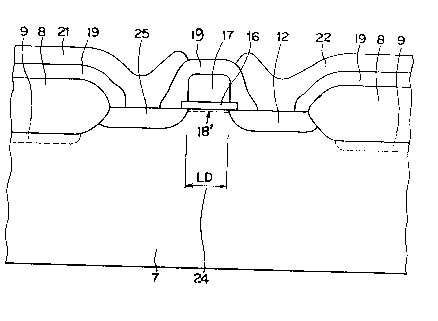
In the figure, reference numeral 7 is a p
conductivity type Si substrate; 8 is a field oxide
film; 9 is a p+ doped region (channel stopper); 10
is an n+ doped region (acting as the source region
S of the enhancement type MOSFET); 11 is another n~
doped region (acting as the drain region D of the enhance-
ment type MOSFET and the source region S of the depletion
type MOSFET formed in a same region); 12 is still another
n+ doped region (acting as the drain region D of the
depletion type MOSFET); 13 is a gate insulating film
for the enhancement type MOSFET; 14. is a gate electrode
for the enhancement type M05FET; 15 is a channel doped
region of the enhancement type MOSFET doped with impurities
of same conductivity as the p conductivity type Si;
16 and 17 are a gate oxide film and a gate electrode
for the depletion type MOSFET, respectively: 18 and
jm:
~~~~~P)>~
18' are channel doped regions of the depletion type
MOSFET doped with impurities of conductivity type opposite
to the p conductivity type Si; 19 is a PSG film (insulating
film); 20 is an electrode
jm:
~J~~~~~3??a
_ 7
.connected electrically with the gate electrode 16 for
the depletion type MOSFET; 21 is an AR, metal wiring
tground line); 22 is an AR metal wiring (source line);
23 represents the channel length of the enhancement type
MOSFET; and 24 represents the channel length of the
depletion type MOSFET.
The gate electrodes 14 and l7~are made of n*
polycrystalline silicon. Ions of impurities such as B,
etc. having the same conductivity type as the p conduc-
tivity type Si substrate 7 are implanted in the channel
doped region 15 just below the gate oxide film 13 for
the enhancement type MOSFET to adjust~the threshold
voltage VthE of the enhancement type MOSFET so as to be
about 0.2 VDD with respect to the source voltage VDD' p
or As ions, which axe impurities having the conductivity
type opposite'to the p conductivity type Si substrate 7
are implanted in the channel doped region 18 just below
the gate oxide film 16 for the depletion type MOSFET to
adjust the threshold voltage VthD of the depletion type
MOSFET sa as to be about -0.6 VDD with respect to the
source voltage VDD.
The electrode 20 connected electrically with the
gate electrode 17 for the depletion type MOSFET is
extended in a~plane perpendicular to the sheet. The
electrode 20 is made of the same material as the gate
electrode for the depletion type MOSFET, i.e. n+
polycrystalline Si. The source of the depletion type
MOSFET and the drain of the enhancement type MOSFET are
connected with the n~ region 11 through the electrode
connected electrically with the gate electrode 17 for
the depletion type MOSFET. The electrode 20 serves
as the output terminal 2 of the inverter circuit indicated
in Figure 7(A).
Figure 10 shows schematically the energy
band in the part of gate electrode G/oxide film OX/p-Si
substrate S of an enhancement type MOSFET. The figure
shows a case where a positive voltage is applied to
the gate electrode and an n type inversion layer as
well as ionized acceptor atoms AT are formed.
Since.the enhancement type MOSFET forms an
n type inverted layer in the surface portion of the
Si substrate by bending electrically the forbidden
band in the surface portion of the p conductivity type
Si substrate by the voltage applied to the gate electrode,
both at the room temperature and at the liquid nitrogen
temperature it. performs the enhancement type operation,
i.e., the threshold voltage VthE remains positive.
Figure 11 shows schematically the energy
band in the part of gate electrode G/oxide film OX/p-Si
substrate S of a prior art depletion type MOSFET, in
which ions such as P, As, etc., which are impurities
of conductivity type opposite to that of the p conductivity
type Si substrate, are implanted. At the room temperature,
since there exists electrons EL due to ionization of
As or P just below the gate oxide film, the MOSFET
described above performs the depletion operation.
In the figure, IO indicates P or As atoms, with which
jm:
~~, ~((/''~~ r
rd ~ :j
-9-
the channel is doped, which are ionized at the room
temperature. However, at 77K, as indicated by IO in
Figure 12, since As or P implanted as opposite conductivity
type impurities is frozen out and not ionized, in the
case where no gate voltage is applied, no n channel
layer is formed just below the gate oxide film 16 and
therefore it does not perform the depletion operation.
That is, the MOSFET, which can perform the depletion
operation owing to the implanted impurities of opposite
conductivity type, performs the enhancement operation
at the liquid nitrogen temperature.
Consequently, there was a problem that although
the prior art inverter of E/D structure using depletion
type MOSFETs including the channel portion 18' doped
with the impurities of opposite conductivity type performs
the normal operation at the room temperature, it cannot
perform the normal operation at the liquid nitragen
temperature.
In the above explanation, no absolute value
of the source voltage VDD for the inverter or the MOSFET
is dealt with. Heretofore, the source voltage for
the MOSFET was determined at 5V, in order to hold the
interchangeability with TTL. However, if the source
voltage is kept at 5V, for a P10SFET having a channel
length smaller than lum, the electric field strength
within the element is increased. Thus, it has become
more and more difficult to secure the normal operation
jm:
-lo-
and the reliability of the MOSFET because of hot carrier
deterioration and drain break down. Consequently,
the source voltage for the integrated circuit cannot
help being decreased. For example, in the case of
a channel length of 0.5um, it is estimated to be about
3.3V and in the case of a channel length of O.lum,
it is estimated to be about 1 to 1.5V.
Therefore, since in the high speed and high
density MOSFET, which is the object of the present
invention, the channel length is necessarily smaller
than lum, the magnitude of the threshold voltage VthD
should be about -2V when the source voltage VDD = 3.3V
and about -0.6 to 0.9V when VDD = 1 to 1.5V.
The MOSFET logic circuit of E/D structure
is characterized in that the fabrication process is
easier and the number of MOSFETs at constructing a
same logic circuit is smaller with respect to the logic
circuit of CMOS structure.
The working speed of the logic circuits remains
almost equal both for the E/D structure and for the
CMO5 structure and it is possible also therefor to
increase the working speed by the operation at the
liquid nitrogen temperature. However, as described
previously, the inverter of E/D structure using depletion
MOSFETs, in which the channel is doped with impurities
of conductivity type opposite to the conductivity type
of the used semiconductor substrate. has a drawback
jm:
-l0A-
that it cannot perform the depletion operation at the
low temperature. because the impurities are frozen
out at that time.
OB~fECT OF THE INVENTION
The object of the present invention is to
provide a MOSFET capable of performing the depletion
operation without doping the channel portion with impurities
of conductivity type opposite to the conductivity type
of the used semiconductor substrate and a method for
lp constructing an inverter of E/D structure using it.
SUMMARY OF THE INVENTION
A MOSFET according to the present invention
is characterized in that 'the surface portion of a semicon-
jm:
11
i' ~ ~~ y.y
doctor body just below an insulating film, on which the
gate electrode. is disposed, is not doped with impurities
of conductivity type opposite to the conductivity type
of the semiconductor substrate, and in the case where
the conductivity type of the semiconductor substrate is
p, the work function of the gate electrode is smaller
than that of the substrate and in the case where the
conductivity type of the substrate is n, the work
function of the gate electrode is greater than that of
the substrate.
BRIEF DESCRIPTIpN OF THE DRAWINGS
Figure 1 is a cross sectional view of an embodi-
ment of the depletion type MOSFET, in which the channel
portion is not doped with impurities of conductivity type
opposite to the conductivity type of the substrate
according to the present invention;
Figure 2 is a graph showing an example of measure-
ments of the high frequency C-V curve for the depletion
type MOSFET according to the present invention;
Figures 3A and 3B are diagrams showing the relation
between the impurity concentration in the substrate, for
which the threshold voltage is negative, and the thickness
of the gate oxide film in the embodiment indicated in
Figure 1;
Figure 4 is a cross sectional view of the n
channel MOSFET inverter of E/D structure, for the depletion
type MOSFET of which the channel is not doped with
impurities of conductivity type opposite to the conduc-
tivity type of the substrate;
Figure 5(A) is a circuit diagram of the E/D
inverter according to the present invention;
Figure 5 (B) is a graph showing an example of
in/out characteristics of the E/D inverter indicated in
Figure 5(A) for a channel length of 0.5um;
Figure 6(A) is a circuit diagram of the E/D
inverter according to the present invention;
Figure 6(B) is a graph showing an example of
in/output characteristics Of the E/D inverter indicated
in Figure 6(A) for a channel length of O.lum;
;~I r? ,'-' r' n ~,
ihr :3 : i
--12-
figure 7(A) is a circuit diagram of a prior
art MOSFET inverter circuit of E/D structure;
Figure 7(B) is a graph showing an example
of in/output characteristics of the prior art MOSFET
inverter of E/D structure indicated in Figure 7(A).
Figure 8 is a graph showing an example of
drain current (ID) vs. gate voltage (VG) characteristics
of a prior art depletion type and a prior art enhancement
type n channel MOSFET; and
Figure 9 is a cross sectional view of a prior
art n channel MOSFET inverter of E/D structures for
the depletion type MOSFET of which the channel is doped
with impurities of conductivity type opposite to the
conductivity type of the substrate:
Figure 10 is a scheme of the energy band
of the part of gate electrode/oxide film/p-Si in the
enhancement type MOSFET;
Figure 11 is a scheme ef the energy band
of the part of gate electrode/oxide film/p-Si in the
prior art depletion type MOSFET~ in which the channel
is doped with impurities of conductivity type opposite
to the conductivity type of the substrate (300K);
Figure 12 is a scheme of the energy band
of the same part as indicated in Figure 11~ cooled
at 77K; and
Figure 13 is a scheme of the energy band
of the part of gate electrode/oxide film/p-Si, in the
jm:
;.
-.13- "~ ° a ~ ;e~ ~ C
case where the gate electrode is made of a metal having
a low work function.
DETAILED DESCRIPTION
If a MOSFET is constructed as described above,
the forbidden band for the surface portion of the substrate
is bent towards the negative side by the difference
in the work function in an energy band diagram using
the electron energy. Therefore, although the surface
portion is not doped with impurities of conductivity
type opposite to that of the substrate, an n type inverted
layer is formed in the surface portion of the substrate.
Since the work function almost does not vary, depending
on the temperature, the n type inverted layer is formed
in the surface portion of the substrate both at the
room temperature and at the liquid nitrogen temperature.
Figure 13 shows a scheme of the energy band
of the part of gate electrode/oxide film/p-Si in the
depletion type MOSFET using a metal having a low work
function. Since the energy band in the p conductivity
type Si is bent by a difference in the work function
between the gate electrode and the p-Si, an n type
channel is formed just below the gate oxide film both
at the room temperature and at 77K, which makes the
depletion operation possible.
Consequently, the MOSFET constructed as described
above can realize the depletion operation both at the
room temperature and at the low temperature.
jm:
.~. J ~y :3 ~~
~,i i.-r d e..~ ~ d ~.J
-14-
Further when an E/D inverter is constructed,
using a depletion type MOSFET constructed as described
above and a prior art enhancement type MOSFET~ it can
perform the inverter operation both at the room temperature
and at the liquid nitrogen temperature. In particular.
at the low temperature, it is possible to realize a
logic circuit having a high switching speed owing to
the increase in the mobility or the saturation speed.
Hereinbelow~ the present invention will be
explained referring to the embodiments indicated in
the drawings.
Figure 1 is a cross sectional view of an
embodiment of the depletion type MOSFET~ in which the
channel portion is not doped with impurities of conductivity
type opposite to the conductivity type of the substrate
according to the present invention.
In Figure 1~ the same reference numerals
as those used for Figure 9 represent identical or similar
parts and 25 is an n~ doped region (the source region
S of the depletion type MOSFET). The surface channel
portion 18' of the Si substrate 17 just below the insulating
film 16 for the gate electrode 17 is not doped with
impurities of conductivity type (n type) opposite to
the conductivity type of the substrate 7. This portion
18' may be doped with impurities of same conductivity
type (p type) as the substrate 7. Further, the gate
electrode 17 is made of a material having a work function
jm:
FJ ~ ~ ~~
-15~-
which is smaller than the work function of the p conductivity
type Si substrate 7. The Si substrate 7 may be of
n conductivity type. In this case, the portion 18'
described above is not doped with~impurities of p conductivity
type and the gate electrode 17 is made of a material
having a work function greater than the work function
of the substrate 7. Also in this case, the portion
corresponding to the portion 18' stated above may be
doped with impurities of same conductivity type as
the n conductivity type substrate.
The basic structure is identical to that
of an enhancement type n channel MOSFET fabricated
by the LOCOS isolation method and the fabrication process
therefor is identical to the well known n channel MOSFET
process. The element isolation may be effected by
any isolation method other than LOCOS isolation method.
e.g. the trench isolation method, if elements can be
isolated thereby.
Further, although the structure indicated
in Figure 1 corresponds to the well known SD (single
drain) structure, it may correspond to the well known
DD (double drain) structure or the LDD (lightly doped
drain). What is essential is that the gate is made
of a metal or a compound having a small work function.
One of the features of the present invention
is that the gate electrode is not made of n+ type polycry-
stalline silicon, but a material having a small work
jm:
rl ~.''
..~ ; J
-16-
function is used therefor. It is required for the
material for the gate electrode to have a work function
smaller than about 4eV.
The inventors of the present invention have
found that although single metals La and Mg as well
as LaB6 in the form of a compound are preferable materials
as concrete materials, LaB6 is especially preferable,
which has a high melting point and is chemically stable.
The melting point of LaB6 is higher than
2000°C and bulk crystals thereof are used as a filament
in an electron beam source. It is known that it is
also chemically stable and has a low work function
as bulk material.
The most undesirable elements in the Si MOSFET
process are alkali metals producing movable ions in
Si02. Further radioactive elements emitting a-rays
are also undesirable elements. The inventors of the
present invention have found that compound materials
consisting of elements, which are widely used in the
prior art Si process or in research and development
and which are thought not to impair the reliability
of Si LSI, can be used also as gate metal.
S7., Ge, B, P, AS, W, Mo, Zr, Ta, T1, Ak r
N, H, Ar, He, etc., can be cited as the elements which
do not impair the reliability of devices, etc., fabricated
in the Si process. Among these elements, metals made
of single elements have work functions higher than
jm:
;.,
fd ar .~ r
-17-
about 4eV and cannot be used as the low work function
gate material for n channel MOSFETs. However, for
example, if compounds such as a nitride, a carbide,
a silicide, etc., have a low work function, they can
be used as the gate material. In general, it is known
that silicides have work functions higher than about
4eV. Therefore, they are unsuitable for realizing
the present invention. Nitrides and carbides have
high melting points and are chemically stable. Therefore,
when they are introduced in the silicon process, they
don't give rise to deteriorations in characteristics
of fabricated MOS devices, etc. However, the work
functions of nitrides and carbides have not been studied
in detail. Further, in the MOSFETs, since they are
used in a thin film state, in order to know whether
they can be applied to the gate metal having a low
work function for the MOSFETs, it is necessary to fabricate
an MOS diode or MOSFET in reality to verify whether
the depletion operation thereof is possible.
The inventors of the present invention have
found that LaB6, nitrides and carbides, which are compounds
having a high adaptability to the prior art Si process
and giving rise to no deteriorations in characteristics,
etc., can be used as the gate metal having a low work
function. As concrete materials, LaB6, nitrides such
as TiN, ZrN, TaN, VN, etc., and carbides such as ZrC,
TiC, TaC, HfC, etc., could be used as the gate metal
having a low work function.
jm:
f 'r'%~~ ~~!
.,I ~ !e! ~7 r.Y d ~~
-18-
In particular, LaB6, TiN, ZrN, TaN and ZrC
have melting points higher than 1500°C and they are
also chemically stable. Further TiN is used already
as a barrier metal in the ohmic junction portion between
A1 or A1-Si and Si also in MOSFET LSIs, for which a
high reliability of level for products in the market
is required, and it is the material most suitable for
depletion type MOSFETs giving rise to no deteriorations
in characteristics.
Thin films of LaB6, TiN, ZrN, TaN and ZrC
can be formed by using the electron beam evaporation
method, the sputtering method, the reactive sputtering
method and the chemical vapor deposition method. In
the present invention, all the thin films could be
formed by the electron beam evaporation method. Further,
it was possible to form thin films of TiN, ZrN and
TaN by the reactive sputtering method in an N2 atmosphere,
using targets made of Ti, Zr and Ta, respectively.
Still further, a TiN film could be formed by the chemical
vapor deposition method, using Ti(N(CH3)2)4 and NH3.
In the following embodiments, LaB6 was fabricated
by using the well-known electron beam evaporation method.
In the following embodiment, TiN, ZrN, TaN and ZrC
films were formed by the reactive sputtering method,
by which the composition control was the easiest.
In a depletion type n channel MOSFET, indicated
in Figure 1, the channel portion just below the gate
jm:
~'1 J iJ '%
~~~d-i;~r.J
-19-
oxide film is not doped with impurities. In the case
where the channel portion is doped with impurities
having a conductivity type opposite to that of the
substrate, the threshold voltage is changed at the
room temperature and 77K, because the impurities, with
which the channel is doped, are frozen out at 77K.
On the other hand, in the case where the channel is
doped with impurities having the same conductivity
type as the substrate, since they are not frozen out,
the threshold voltage remains almost unchanged at the
room temperature and 77K.
For example, when the impurity concentration
in the p conductivity type Si substrate was about
1 x 1016 cm-3, the gate oxide film was about 20 nm
thick and an LaB6 gate electrode was used as the gate
metal, the threshold voltage of the MOSFET was about
-1.6 v. On the other hand, e.g., when the impurity
concentration in the p conductivity type Si substrate
was about 1 x 1016cm 3, the gate oxide film was about
~0 20 nm thick and Ti.N was used as the gate metal, the
threshold voltage of the MOSFET was about -1.2 Y.
When the channel was doped with impurities having the
same conductivity type as the substrate, it was possible
to vary the threshold voltage in the positive direction
e.g., to -1.0 1i or -0.5 V by increasing the amount
of the channel dope.
jm:
S/'S I,~! 1°,a
d i~.A ~;.Y J
-20-
Although, in Figure l, the gate metal is
formed by one layer of e.g., LaB6 or TiN, another layer
made of polycrystalline Si, high melting point metal
or silicide may be formed on the LaB6 or TiN layer.
The resistivity of the thin film made of LaB6, TiN,
ZrN, TaN or ZrC is as high as several tens or several
hundreds of 1.~~-cm. When a film made of a metal, whose
resistivity is several u~-cm, or a silicide, whose
resistivity is 10 to several 10 u~-cm, is formed on
the film of LaB6, TiN, ZrN, TaN or ZrC, the effective
resistivity of the gate electrode was able to be effectively
reduced. In the case where the material for the gate
electrode is used as wiring metal, as it is, in a complicated
logic circuit for the reason of the process, the gate
structure of two or three layers is a desirable structure
for low resistance wiring. What is essential is to
form a material having a low work function just below
the gate oxide film.
In the case of the MOSFET, the threshold
voltage is shifted, depending on the interfacial fixed
charge density. However, in the case of the n channel
MOSFET, since the threshold voltage increases in the
negative direction, if the interfacial fixed charge
density is high, it is never driven in the enhancement
operation owing to the high interfacial fixed charge
density.
jm:
~~ ;~ ~ ;~~ o r
~~i~ ~~f,~~
-21
As described above, although the threshold
voltage is negative for the n channel MOSFET, for the
inverter of E/D structure, the magnitude of the threshold
voltage is a problem. For the inverter of E/D structure,
the threshold voltage VINV of the inverter is defined
as a voltage, for which the output voltage Vout is
equal to the input voltage Vin in the inverter characteristics
indicated in Figure 7(B). By a well-known designing
method, the threshold voltage of the inverter is set
at about -0.6 VDD so that the switching speed remains
approximately equal at the turning-on and the turning-off
of the input voltage at about 1/2 of the source voltage
VDD of 'the inverter. Consequently, in the case where
the source voltage VDD is 5V, the threshold voltage
of the depletion type MOSFET is about -3V.
In the ultra-high speed high density MOSFET
logic circuit, which is the object of the present invention,
since it is composed of fine MOSFETs, whose channel
length is smaller than about 0.5 um, the threshold voltage
is about 3.3V, when the channel length is about 0.5~.an,
and 1 to 1.5V, when it is about O.lum. Therefore,
the threshold voltage of the depletion type MOSFET
should be set at about -2V, when the channel length
is about 0.5um, and -0.6 to -1.OV, when it is O.lum.
In a depletion MOSFET using LaB6, TiN, ZrN,
TaN or ZrC, the lower limit of the threshold voltage
obtained, when the impurity concentration in the p
conductivity type substrate was as low as e.g.,
jm:
~i
-22- ~:~ f~ ~, :s :r ~~ ~.~
1 x 1015cm 3 and the gate oxide film was as thin as
about 5 nm~ was about -2V. Furthers even if the thickness
of the gate oxide film was constants it was possible
to control the gate voltage in a region from -2V to
OV by implanting B ions etc.~ which are impurities
having the same conductivity type as the p conductivity
type substrates in the channel portion. Consequently
the depletion type MOSFET according to the present
invention can be used for the inverter of E/D structure
using fine MOSFETs~ whose channel length is smaller
than 0.5um, in which the gate oxide film should be
as thin as about 5 to 20nm and the source voltage should
be as low as about 1 to 3.3V.
Fig. 4 is a schematical cross sectional view
of an inverter having the E/D structure using LaB6
or TiN or ZrN or TaN or ZrC for the gate metal.
In the figures the reference numerals identical
to those indicated in Figures l, 5, and 9, represent
identical or corresponding items and 26 is the channel
portion of the depletion type MOSFET~ which is not
doped with impurities of conductivity type opposite
to the conductivity type of the substrate.
As the fabrication process of the embodiment
described above, the n MOS process using the well known
LOCOS isolation technique was used. The isolation
may be effected by using any method other than the
LOCOS isolation method. It is required only to be
jm:
-23-
able to isolate different elements. However, contrary
to the well known MOS process, the part of the p conductivity
type Si 26 just below the gate oxide film 16 in the
depletion type n channel MOSFET is not doped by the
ion implantation, etc., with impurities such as As
and P having the opposite conductivity type. TiN or
TaN or ZrN or ZrC was formed by using the reactive
sputtering method. LaB6 was formed by using the well
known electron beam evaporation method. Although,
in Figure 4, the gate metal is of one-layered structure
made of '.Girl, etc., polycrystalline silicon, a high
melting point metal, silicide, etc.,may be formed on
the layer rnade of TiN, eta., so that the gate electrode
is of two- or three-layered structure. Hlhat is essential
is that LaB6 or TiN or ZrN or TaN or ZrC, which is
a metal having a low work function, is formed directly
on the oxide film. The source and the drain region
of the depletion type n channel MOSFET was formed by
implanting ions of P after the formation of the gate
electrode.
Further, for the gate electrode 14 of the
enhancement type MOSFET, the conventional n+ polycrystalline
Si was used.
The gate. electrode of the enhancement type
MOSFET may be not of one-layered structure made of
n+ type polycrystalline Sir but of polycide structure,
in which a si7.icide layer is formed on the n+ type
jm:
_24_ ~, t~' ~ ! 'G ~,a Cj
polycrystalline Si layer. Further not n+ type polycrystalline
Si, but silicides of W, Ti, Ta, etc., may be used
for the gate metal. High melting point metals such
as Mo, W, etc., may be also used therefor. Furthermore,
AR may be used therefor.
In order to control the threshold voltage
of the enhancement type MOSFET, ions of B, which
are impurities of same conductivity type as the p
conductivity type Si, were implanted in the channel
portion before the formation of the gate oxide film
13. The ions of B were implanted so that the threshold
voltage VthE is about 0.7 V for a MOSFET having a
channel length of about 0.5 um and the threshold
voltage VthE is about +0.3V for a MOSFET having a
channel length of O.lum.
On the other hand, in order to control
the threshold voltage of the depletion type MOSFET,
ions of B, which are impurities of same conductivity
type as the p conductivity type Si substrate, were
implanted in the channel portion before the formation
of the gate oxide film 2. The ions of B were implanted
so that the threshold voltage VthD is about -1.5
to -2V for a MOSFET having a channel length of 0.5 um
and the threshold VthD is about -1V for a MOSFET
having a channel length of O.lum.
Although in the present embodiment impurities
of same conductivity type as the p conductivity type
Si were implanted for the control of the threshold
sd/~. -;
25
r.3r~~.~
voltage, the ion implantation is not necessarily
effected, if the threshold voltages of the enhancement
type MOSFET and the depletion type MOSFET are about
0.2VDD and about -0.6VDD, respectively, with respect
to the source voltage VDD of the E/D inverter.
If ions of P or As, which are impurities
of conductivity type opposite to the p conductivity
type Si, were implanted in the channel portion at
the fabrication of the depletion type MOSFET according
to the prior art technique, although an n type channel
is formed, which performs the depletion type operation
at the room temperature, at the liquid nitrogen temperature
(77K), since P or As impurities implanted as n conductivity
type impurities would be exhausted, no n type channel
layer would be formed and it would not perform the
depletion type operation. However, in the case where
the channel portion is doped with impurities of p
conductivity type with respect to the p conductivity
type Si only for the purpose of varying the concentration
thereof, since they are not frozen out, the freeze
out described previously has influences neither at
the room temperature nor at 77K. Therefore the E/D
inverter according to the present embodiment was
able to perform the normal inverter operation both
at the room temperature and at 77K.
Contrary to the fact that the E/D inverter
using conventional depletion type MOSFETs performed
no normal operation at 77K, the E/D inverter according
sd/
I~ ~.~ ~J ~~i
:.,. ~. ~.a a . y G~ -..
to the present invention performed the normal operation
both at the room temperature and at 77K.
A ring oscillator was constructed by connecting
E/D inverters described above in a mufti-stage form
and the gate delay time per gate was measured at
the room temperature and at 77K. It was found that
it was shortened about 0.7 to 0.5 time at 77K with
respect to that obtained at the room temperature.
For realizing the present invention. LaB6,
TiN, ZrN, TaN and ZrC, which are materials easily
fitted to the conventional silicon process, were
used.
In the MOSFET fabricated by using these
materials, even after a high temperature accelerated
deterioration test at about 175oC, no variations
in the flat band voltage of the MOS diode. the threshold
voltage of VthD of the FET and in the mutual conductance
gm were found. Further another high temperature
accelerated deterioration test at about 175°C was
effected also for a ring oscillator, in which the
inverters described previously were connnected in
series, and neither variations in the threshold voltage
Vth of the inverter nor deteriorations in the delay
time at the room temperature and 77K were observed
after the test.
(EMBODIMENT 1)
A depletion type n channel MOSFET having
the cross sectional structure as indicated in Figure '
sd/.'
s ~., ,
-27- ~ ~ r~.~ ~3 "~
1 was fabricated by using LaB6 for the gate electrode.
LaB6 was formed by the electron beam evaporation
method. The LOCOS structure is used for the element
isolation and the fabrication process is the well
known self-alignment type n MOS process. After the
formation of the gate electrode As ions were implanted
to form the source and the drain regions.
The impurity concentration in the p conductivity
type Si substrate was about 1 x 1016cm-3; the gate
oxide film was about 20 nm thick; and the channel
length was about lum. 6 sorts of MOSFETs were fabricated,
in which the thickness of the gate electrode was
at 6 levels i.e. 20, 50~ 100 200 500 and 1000
nm.
Figure 2 is a graph showing results of
measurements of the high frequency C-V curve of an
MIS diode between the gate electrode 17 and the p
conductivity type Si substrate 7 for a frequency
of about lMHz at temperatures of 300K and 77K. The
threshold voltages at which the surface portion of
the p conductivity type Si substrate of this MIS
diode was inverted was about -1.6V. The C-V characteristics
were not changed at the room temperature and 77K.
Further the C-V characteristics indicated in Figure
2 didn't depend on the thickness of the gate electrode.
The drain current (ID) vs. gate voltage
(V~) characteristics of the fabricated MOSFET were
those of the depletion type n channel MOSFET indicated
sd/
a o; r tj
., w
_2$_
in Figures 6(A) and 6(B) and the threshold voltage
VthD of the MOSFET was about -1.6V at the room temperature.
The variation in the threshold voltage was smaller
than 0.2V even at 77K. The current-voltage characteristics
of the MOSFET didn't depend on the thickness of the
gate electrode.
MOSFETs having various thicknesses of the
gate oxide film and various impurity concentrations
in the p conductivity type Si substrate were fabricated
the thickness of the gate electrode being kept constant
at 500 nm. The thicknesses of the gate oxide film
were 5~ 10~ 20, 40~ 60~ 100 120 and 140 nm and the
impurity concentrations in the substrate were
1 x 10¹⁵, 2 x 10¹⁵ 5 x 10¹⁵ 1 x 10¹⁶ 2 x 10¹⁶
5 x 101, 1 x 10¹⁷, 2 x 10¹⁷ 5 x 10¹⁷ 1 x 10¹⁸
and 2 x 1018cm 3, MOSFETS of all the possible combinations
thereof being fabricated. Fig 3(A) shows the relation
between the thickness Tox of the gate oxide film
at which the threshold voltage is turned to a negative
values and the impurity concentration NA of the p
conductivity type Si substrate. When the thickness
of the gate oxide film and the impurity concentration
are in a region below the respective line (hatched
region) in Fig. 3(A), the threshold voltage was turned
to be negative. In the case where the impurity concentration
in the p conductivity type substrate was as small
as 1 x 1015cm 8 and the thickness of the gate oxide
film was as small as 5 nm~ the lower limit of the
sd/-,~
6; n~ ,., ,.~ i r ~ h
-.~ l~ r~ ~l 'r r ,~.a i..l
-29-
threshold voltage was about -2V. The interfacial
fixed charge density of the fabricated MOS diode
described by referring to Figures 2 and 3(A) in the
present embodiment was 1 to 5 x lOlOcm-2.
(EMBODIMENT 2)
An inverter of E/D structure having the
cross sectional structure as indicated in Figure
4, using LaB6 for the gate electrode of the depletion
type MOSFET and n~ type polycrystalline silicon for
the gate electrode of the enhancement type MOSFET
and a ring oscillator, in which inverters thus fabricated
were connected in series. were fabricated. The channel
length was 0.1 um or 0.5um both for the depletion
type and for the enhancement MOSFET. LaB6 was formed
by using the electron beam evaporation method and
the n+ type polycrystalline silicon was formed by
the well known CVD method. The LOCOS structure is
used for the element isolation and the fabrication
process is the well known self-alignment type in
MOS process. After the formation of the gate electrode
As ions were implanted to form the source and the
drain regions. Ions were implanted in the channel
portion for the control of the threshold voltage.
B ions were implanted in the channel portion of the
enhancement MOSFET before the formation of the n+
type polycrystalline silicon gate so that the threshold
voltage of the enhancement MOSFET having a channel
length of 0.5um was about 0.7V and the threshold
sd/, :;,
.;
-3p- ~; ~. ' ,i ~J '% ')
n
' J ~a
voltage of the enhancement type MOSFET having a channel
length of 0.5um was about 0.3V. On the other hand,
B ions, which are impurities of same conductivity
type as the p conductivity type Si substrate, are
implanted in the channel portion of the depletion
type MOSFET before the formation of the LaB6 gate
so that the threshold voltage of the depletion type
MOSFET having a channel length of 0.5um was about
-1.6V and the threshold voltage of the enhancement
type MOSFET having a channel length of O.lum was
about -1V.
Figures 5(A) and 6(A) show input voltage-output
voltage characteristics of the inverter having the
E/D structure using MOSFETs, whose channel lengths
are 0.5um and O.lum, respectively. The source voltage
was 3.3V for the 0.5Wn MOSFET and 1.5V for the O.lum
MOSFET. The input-output voltage characteristics
as indicated in Figs. 5(A) and 6(A) were obtained
both at the room temperature and at 77K.
The gate delay time per gate of the ring
oscillator was measured and it was found that at
77K it was about 0.7 time as short as that obtained
at the room temperature.
(EMBODIMENT 3)
A depletion type MOSFET similar to that
described in EMBODIMENT 1 was fabricated by replacing,
the gate electrode made of LaB6 in EMBODIMENT 1 by
TiN. TiN was formed by using the reactive sputtering
sd/ .
%;
31- ~~w~~;~l.zF~
method.
The obtained C-V characteristics and the
current-voltage characteristics of the MOSFET were
similar to those obtained in EMBODIMENT 1. Figure
3(B) shows the relation between the thickness of
the gate oxide film, at which the threshold voltage
is turned to a negative value, and the impurity concentration
of the p conductivity type Si substrate. Similarly
to that described in EMBODIMENT 1, when the thickness
of the gate oxide film and the impurity concentration
in the substrate are in a region below the respective
line (hatched region) in Figure 3(B), the threshold
voltage was turned to be negative. In the case where
the impurity concentration in the p conductivity
type substrate was as small as 1015 cm 3 and the
thickness of the gate oxide .film was as small as
5nm, the lower limit of the threshold voltage was
about -1.6V. The interfacial fixed charge density
of the fabricated MOS diode described by referring
to Figures 2 and 3(B) in the present embodiment was
1 to 5 x lOlOcm 2.
(EMBODIMENT 4)
An inverter of E/D structure having the
cross sectional structure as indicated in .Figure
4, by the process similar to that described in EMBODIMENT
2, using TiN for the gate electrode of the depletion
type MOSFET and n+ type polycrystalline silicon for
the gate electrode of the enhancement type D70SFET
sd/,.
~>
f.~ n. ,~ :f ~ y G.s C)
and a ring oscillatory in which inverters thus fabricated
were connected in series, were fabricated.
TiN was formed by using the reactive sputtering
method and the n+ type polycrystalline silicon was
formed by the well known CVD method. Ions were implanted
in the channel portion for the control of the threshold
voltages similarly to EMBODIMENT 2.
Similarly to EMBODIMENT 2, for the MOSFETs
having channel lengths of 0.5um and O.lum the input
voltage-output voltage characteristics of the inverters
of E/D structure. as indicated in Figs. 5(A) and
6(A) respectively were obtained. The source voltage
was 3.3V for the 0.5um MOSFET and 1.5V for the O.lum
MOSFET. The input-output voltage characteristics
as indicated in Figures 5(A) and 6(A) were obtained
both at the room temperature and at 77K.
The gate delay time per gate of the ring
oscillator was measured and it was found that at
77K it was about 0.7 time as short as that obtained
at the room temperature.
(EMBODIMENT 5)
A depletion type MOSFET similar to that
described in EMBODIMENT 1 was fabricated by replacing
the gate electrode made of LaB6 in EMBODIMENT 1 by
ZrN. ZrN was formed by using the reactive sputtering
method.
The obtained C-V characteristics and the
current-voltage characteristics of the MOSFET were
sd/ ',
-33-
p
i ~ ~ ! ~, y ,,, ,:.J
similar to those obtained in EMBODIMENT 1.
Figure 3(B) shows the relation between
the thickness of the gate oxide film, at which the
threshold voltage is turned to a negative value,
and the impurity concentration of the p conductivity
type Si substrate. Similarly to that described in
EMBODIMENT l, when the thickness of the gate oxide
film and the impurity concentration are in a region
below the respective line (hatched region) in Figure
3(B), the threshold voltage was turned to be negative.
In the case where the impurity concentration in the
p conductivity type substrate was as small as 1015cm 3
and the thickness of the gate oxide film was as small
as 5 nm, the lower limit of the threshold voltage
was about -2.4V. The interfacial fixed charge density
of the fabricated MOS diode described by referring
to Figures 2 and 3(B) in the present embodiment was
1 to 5 x lOlOcm 2.
(EMBODIMENT 6)
An inverter of E/D structure having 'the
cross sectional structure as indicated in Figure
4, by the process similar to that described in EMBODIMENT
2, using ZrN for the gate electrode of the depletion
type MOSFET and n+ type polycrystalline silicon for
the gate electrode of the enhancement type MOSFET
and a ring oscillator, in which inverters thus fabricated
were connected in series. were fabricated.
ZrN was formed by using the reactive sputtering
sd/';f
-34- ~' s~ ~., a.. ~... n ~->
f ~ i ~ ~: i ~ !,
method and the n+ type polycrystalline silicon was
formed by the well known CVD method. Tons were implanted
in the channel portion for the control of the threshold
voltages similarly to EMBODIMENT 2.
Similarly to EMBODIMENT 2, for the MOSFETs
having channel lengths of 0.5um and 0.1 um the input
voltage-output voltage characteristics of the inverters
of E/D structures as indicated in Figs. 5(A) and
6(A)i respectively were obtained. The source voltage
was 3.3V for the 0.5um MOSFET and 1.5V for the O.lum
MOSFET. The input-output voltage characteristics
as indicated in Figures 5(A) and 6(A) were obtained
both at the room temperature and at 77K.
The gate delay time per gate of the ring
oscillator was measured and it was found that at
77K it was about 0.7 time as short as that obtained
at the room temperature.
(EMBODIMENT 7)
A MOSFET was fabricated by replacing the
gate metal LaB6 in EMBODIMENT 1 by TaN. TaN was
formed by using the reactive sputtering method.
The obtained C-V characteristics and the
current-voltage characteristics of the MOSFET were
similar to those obtained in EMBODIMENT 1. Figure
3(B) shows the relation between the thickness of
the gate oxide filmy at which the threshold voltage
is turned to a negative values and the impurity concentration
of the p canductivity type Si substrate. Similarly
sd/~ ,''
-3 5- ~,,, r,.. r,. .) ;7
r r ~ ~,Wa
~ ~' r.J
to that described in EMBODIMENT 1, when the thickness
of the gate oxide film and the impurity concentration
in the substrate are in a region below the respective
line (hatched region) in Figure 3(B), the threshold
voltage was turned to be negative. In the case where
the impurity concentration in the p conductivity
type substrate was as small as 1015cm 3 and the thickness
of the gate oxide film was as small as 5 nm, the
lower limit of the threshold voltage was about -2.4V.
The interfacial fixed charge density of the fabricated
MoS diode described by referring to Figures 2 and
3(B) in the present embodiment was 1 to 5 x lOlOcm 2.
(EMBODIMENT 8)
An inverter of E/D structure having the
cross sectional structure as indicated in Figure
4, by the process similar to that described in EMBODIMENT
2, using TaN for the gate electrode of the depletion
type MOSFET and n+ type polycrystalline silicon for
the gate electrode of the enhancement type MOSFET .
and a ring oscillator, in which inverters thus fabricated
were connected in series, were fabricated.
TaN was formed by using the reactive sputtering
method and the n~ type polycrystalline silicon was
formed by the well known CVD method. Ions were implanted
in the channel portion for the control of the threshold
voltage, similarly to EMBODIMENT 2.
Similarly to EMBODIMENT 2, for the MOSFETs
having channel lengths of 0.5um and O.lum the input
sd/
_36- s~ t _r'' ';~,f .: s~ o.'s
:~ :~ ~s
voltage-output voltage characteristics of the inverters
of E/D structures as indicated in Figs. 5(A) and
6(A)~ respectively were obtained. The source voltage
was 3.3V for the 0.5um MOSFET and 1.5V for the O.lu m
MOSFET. The input-output voltage characteristics
as indicated in Figures 5(A) and 6(A) were obtained
both at the room temperature and at ?7K.
The gate delay time per gate of the ring
oscillator was measured and it was found that at
77K it was about 0.7 time as short as that obtained
at the room temperature.
(EMBODIMENT 9)
A depletion type MOSFET similar to that
described in EMBODIMENT 1 was fabricated by replacing
the gate electrode made of LaB6 in EMBODIMENT 1 by
ZrC. ZrC was formed by using the reactive sputtering
method.
The obtained C-V characteristics and the
current-voltage characteristics of the MOSFET were
similar to those obtained in EMBODIMENT 1.
Figure 3(B) shows the relation between
the thickness of the gate oxide filmy at which the
threshold voltage is turned to a negative value,
and the impurity concentration of the p conductivity
type Si substrate. Similarly to that described in
EMBODIMENT 1~ when the thickness of the gate oxide
film and the impurity concentration are in a region
below the respective line (hatched region) in Figure
sd/~,;
3(B), the threshold voltage was turned to be negative.
In the case where the impurity concentration in the
p conductivity type substrate was as small as 1015cm
and the thickness of the gate oxide film was as small
as 5 nm, the lower limit of the threshold voltage
was about -2.4v. The interfacial fixed charge density
of the fabricated MOS diode described by referring
to Figures 2 and 3(B) in the present embodiment was
1 to 5 x lOlOcm-2.
(EMBODIMENT 10)
An inverter of E/D structure having the
cross sectional structure as indicated in Figure
4, by the process similar to that described in EMBODIMENT
2, using ZrC for the gate electrode of the depletion
type MOSFET and n+ type polycrystalline silicon for
the gate electrode of the enhancement type MOSFET
and a ring oscillator, in which inverters thus fabricated
were connected in series, were fabricated.
ZrC was formed by using the reactive sputtering
method and the n+ type polycrystalline silicon was
formed by the well known CVD method. Ions were implanted
in the channel portion for the control o~ the threshold
voltage, similarly to EMBODIMENT 2.
Similarly to EMBODIMENT 2, for the MOSFETs
having channel lengths 0.5um and O.l~m the input
voltage-output voltage characteristics of the inverters
of E/D structure. as indicated in Figs. 5(A) and
6(A), respectively, were obtained. The source voltage
sd/,~,,
-38-
i, A :M h.~ ~,,
~Y hd ~ o f øy
was 3.3V for the 0.5um MOSFET and 1.5V for the O.lum
MOSFET. The input-output voltage characteristics
as indicated in Figures 5(A) and 6(A) were obtained
both at the room temperature and at 77K.
The gate delay time per gate of the ring
oscillator was measured and it was found that at
77K it was about 0.7 time as short as that obtained
at the room temperature.
(EMBODTMENT 11)
In EMBODIMENTS 1 and 2, the gate electrode
of the depletion type MOSFET was of one-layered structure
made of LaB6. A depletion type MOSFET having a gate
of two-layered structure was fabricated by forming
a W or Mo or titanium silicide or wolfram silicide
film after the formation of the gate electrode made
of LaB6. The film made of W or Mo or titanium silicide
or wolfram silicide on the LaB6 layer was 800 nm
thick. MOSFETs having the LaB6 layer of various
levels of the thickness of 10, 20, 50 and 100 nm
were fabricated. The W or Mo or titanium silicide
or wolfram silicide film was formed by the well known
sputtering method.
The MOS diode characteristics, the characteristics
of the depletion type MOSFET, the result indicated
in Fig. 3(B), the characteristics of the inverter
and the characteristics of the ring oscillator, which
are obtained. were identical to those described in
EMBODIMENTS 1 and 2, independently of the W or Mo
sd/~,~;
-39-
or titanium silicide or wolfram silicide film formed
~~ t-~ ro' ° : s ra ~.~
on the LaB6 layer.
(EMBODIMENT 12)
In EMBODIMENTS 3 and 4, the gate electrode
of the depletion type MOSFET was of one-layered structure
made of TiN. A depletion type MOSFET having a gate
of two-layered structure was fabricated by forming
a W or Mo or titanium silicide or wolfram silicide
film after the formation of the gate electrode made
of TiN. The film made of W or Mo or titanium silicide
or wolfram silicide on the TiN layer was 800 nm thick.
MOSFETs having the TiN layer of various levels of
the thickness of 10, 20, 50 and 100 nm were fabricated.
The W or Mo or titanium silicide or wolfram silicide
film was formed by the well known sputtering method.
The MOS diode characteristics, the characteristics
of the depletion type MOSFET, the result indicated
in Fig. 3(B), the characteristics of the inverter
and the characteristics of the ring oscillator, which
are obtained, were identical to those described in
EMBODIMENTS 3 and 4, independently of the W or Mo
or titanium silicide or wolfram silicide film formed
on the TiN layer.
(EMBODIMENT 13)
In EMBODIMENTS 5 and 6, the gate electrode
of the depletion type MOSFET was of one-layered structure
made of ZrN. A depletion type MOSFET having a gate
of two-layered structure was fabricated by forming
s d / ~-~
_40, ~J ,rl: i ;°. G) C~
~r if sd t: ..y ;.
a W or Mo or titanium silicide or wolfram silicide
film after the formation of the gate electrode made
of ZrN. The film made of W or Mo or titanium silicide
or wolfram silicide on the ZrN layer was 800 nm thick.
MOSFETs having the ZrN layer of various levels of
the thickness of 10, 20, 50 and 100 nm were fabricated.
The W or Mo or titanium silicide or wolfram silicide
film was formed by the well known sputtering method.
The MOS diode characteristics, the characteristics
of the depletion type MOSFET, the result indicated
in Fig. 3(B), the characteristics of the inverter
and the characteristics of the ring oscillator, which
are obtained, were identical to those described in
EMBODIMENTS 3 and 4, independently of the W or Mo
or titanium silicide or wolfram silicide film formed
on the ZrN layer.
(EMBODIMENT 14)
In EMBODIMENTS 7 and 9, the gate electrode
of the depletion type MOSFET was of one-layered structure
made of TaN. A depletion type MOSFET having a gate
of two-layered structure was fabricated by forming
a W or Mo or titanium silicide or wolfram silicide
film after the formation of the gate electrode made
of TaN. The film made of W or Mo or titanium silicide
or wolfram silicide on the TaN layer was 800 nm thick.
MOSFETs having the TaN layer of various levels of
the thickness of 10, 20, 50 and 100 nm were fabricated.
The W or Mo or titanium silicide or wolfram silicide
sd/ ~'
>~
-41- r~ ,. ~ ,.,
C, ~;~ s .~~ <,
film was formed by the well known sputtering method.
The MOS diode characteristics the characteristics
of the depletion type MOSFET~ the result indicated
in Fig. 3(B)~ the characteristics of the inverter
and the characteristics of the ring oscillatory which
are obtained, were identical to those described in
EMBODIMENTS 5 and 6, independently of the W or Mo
or titanium silicide or wolfram silicide film formed
on the TaN layer.
(EMBODIMENT 15) ,
In EMBODIMENTs 7 and 8, the gate electrode
of the depletion type MOSFET was of one-layered structure
made of ZrC. A depletion type MOSFET having a gate
of two-layered structure was fabricated by forming
a W or Mo or titanium silicide or wolfram silicide
film after the formation of the gate electrode made
of ZrC. The film made of W or Mo or titanium silicide
or wolfram silicide on the ZrC layer was 800 nm thick.
MOSFETs having the ZrC layer of various levels of
the thickness of 10, 20, 50 and 100 nm were fabricated.
The W or Mo or titanium silicide or wolfram silicide
film was formed by the well known sputtering method.
The MOS diode characteristics, the characteristics
of the depletion type MOSFET~ the result indicated
in Fig. 3(B)~ the characteristics of the inverter
and the characteristics of the ring oscillatory which
are obtained were identical to those described in
EMBODIMENTS 7 and 8, independently of the W or Mo
sd/ ,.:'
F'~ n
r.; ~'; ',' .: ~ ~~ ,~
-42-
or titanium silicide or wolfram silicide film formed
on the ZrC layer.
(EMBODIMENT 16)
The gate metal of the depletion type MOSFET
in the inverter of E/D structure and the ring oscillator
described in EMBODIMENTs 2 and 11 was of one-layered
structure made of LaB6 or two-layered structure made
of LaB6 and another material (W or Mo or titanium
silicide or wolfram silicide). On the other hand,
the gate metal of the enhancement type MOSFET was
made of n+ type polycrystalline Si in all the cases.
Inverters of E/D structure and ring oscillators
were fabricated by using W or Mo or titanium silicide
or wolfram silicide for the gate metal of the enhancement
type MOSFET described in EMBODIMENTS 2 and 11. W
or Mo or titanium silicide or wolfram silicide was
formed by the well known sputtering method.
Results similar to those described in EMBODIMENTS
2 and 11 were obtained for the characteristics of
the inverters and the characteristics of the ring
oscillators which were obtained independently of
the sort of the gate metal of the enhancement type
MOSFET.
(EMBODTMENT 17)
The gate metal of the depletion type MOSFET
in the inverter of E/D structure and the ring oscillator
described in EMBODIMENTS 4 and 12 was of one-layered
structure made of TiN or two-layered structure made
sd/-,°~
c~~?~:y~~r y.pn
~~~ i7 i~ ~~ : ~ 6a 3
of TiN and another material (W or Mo or titanium
silicide or wolfram silicide). On the other hand
the gate metal of the enhancement type MOSFET was
made of n+ type polycrystalline Si in all the cases.
Inverters of E/D structure and ring oscillators
were fabricated by using W or Mo or titanium silicide
or wolfram silicide for the gate metal of the enhancement
type MOSFET described in EMBODIMENTS 4 and 12. W
or Mo or titanium silicide or wolfram silicide was
formed by the well known sputtering method.
Results similar to those described in EMBODIMENTs
4 and 12 were obtained for the characteristics of
the inverters and the characteristics of the ring
oscillators, which were obtained independently of
the sort of the gate metal of the enhancement type
MOSFET.
(EMBODIMENT 18)
The gate metal of the depletion type MOSFET
in the inverter of E/D structure and the ring oscillator
described in EMBODIMENTS 6 and 13 was of one-layered
structure made of ZrN, or two-layered structure made
of ZrN and another material (W or Mo or titanium
silicide or wolfram silicide). On the other hand
the gate metal of the enhancement_type MOSFET Was
made of n+ type polycrystalline Si in all the cases.
Inverters of E/D structure and ring oscillators
were fabricated by using W or Mo or titanium silicide
or wolfram silicide for the gate metal of the enhancement
s d/, ;~,,
.. . . , _ .. . . .: . , . . . . . ,.: -.. . " .
,. z . .... . , ,. . . .. .
~.., r . ~w ~. S> !'.
1 c e.~ ,~ . ~ i,: ~.)
-44-
type MOSFET described in EMBODIMENTS 6 and 13. W
or Mo or titanium silicide or wolfram silicide was
formed by the well known sputtering method.
Results similar to those described in EMBODIMENTs
6 and 13 were obtained for the characteristics of
the inverters and the characteristics of the ring
oscillators, which were obtained independently of
the sort of the gate metal of the enhancement type
MOSFET.
(EMBODIMENT 19)
The gate metal of the depletion type MOSFET
in the inverter of E/D structure and the ring oscillator
described in EMBODIMENTS 8 and 14 was of one-layered
structure made of TaN or two-layered structure made
of TaN and another material (W or Mo or titanium
silicide or wolfram silicide). On the other hand
the gate metal of the enhancement type MOSFET was
made of n~ type polycrystalline Si in all the cases.
Inverters of E/D structure and ring oscillators
were fabricated by using W or Mo or titanium silicide
or wolfram silicide for the gate metal of the enhancement
type MOSFET described in EMBODIMENTS 8 and 14. W
or Mo or titanium silicide or wolfram silicide was
formed by the well known sputtering method.
Results similar to those described in EMBODIMENTS
8 and 14 were obtained for the characteristics of
the inverters and the characteristics of the ring
oscillators which were obtained independently of
sa/l~3
6~, ~ / .::J F~ G7 !')
ti ~d ~ ~.. !~d ',J
-45
the sort of the gate metal of the enhancement type
MOSFET.
(EMBODIMENT 20)
The gate metal of the depletion type MOSFET
in the inverter of E/D structure and the ring oscillator
described in EMBODIMENTS 10 and 15 was of one-layered
structure made of ZrC or two-layered structure made
of ZrC and another material (W or Mo or titanium
silicide or wolfram silicide). On the other hand
the gate metal of the enhancement type MOSFET was
made of n+ type polycrystalline Si in all the cases.
Inverters of E/D structure and ring oscillators
were fabricated by using W or Mo or titanium silicide
or wolfram silicide for the gate metal of the enhancement
type MOSFET described in EMBODIMENTs 10 and 15.
W or Mo or titanium silicide or wolfram silicide
was formed by the well known sputtering method.
Results similar to those described in EMBODIMENTS
10 and 15 were obtained for the characteristics of
the inverters and the characteristics of the ring
oscillators which were obtained independently of
the sort of the gate metal of the enhancement type
MOSFET.
(EMBODIMENT 21)
Although, in the above embodiments, p conductivity
type Si was used for the substrates also in the case
where n conductivity type Si was used it was possible
to fabricate a depletion type p channel MOSFET and
':a
sd/f,.,..
~~ii~i >~..,~~ 3
-46-
an inverter of E/D structure without doping the channel
portion of the depletion type MOSFET with B atoms
which are impurities of conductivity type opposite
to n conductivity type Si. Although Se. Ir. Pty
etc.~ which are substances whose work function is
greater than about 5.5 eVr among substances whose
work function is greater than that of the n conductivity
type Si, can be used for the gate electrode of the
depletion type p channel MOSFET, it is desirable
to use Pt therefore which can be formed easily by
the electron beam evaporation method, etc. and which
has a melting point of about 1770°C. It was possible
to obtain a depletion type MOSFET and a p channel
inverter of E/D structure performing the depletion
operation both at the room temperature and at the
low temperature by using platinum for the gate electrode.
The depletion type MOSFET according to
the present invention can be operated both at the
room temperature and at the liquid nitrogen temperature
and the inverter of E/D structure can be operated
also both at the room temperature and at the liquid
nitrogen temperature.
The MOSFET integrated circuit using depletion
type MOSFETs and inverters of E/D structure according
to the present invention can provide a high speed
and high density integrated circuit having the high
speed of an integrated circuit using bipolar transistors
and a high degree of integration of MOSFETs together
sd/~.~,,
".~ ~,~ Cl~
~~ fa ~ ~~'s ~~ 6H ~)
by driving it at the liquid nitrogen temperature.
Further the inverter of E/D structure can
provide a high speed and high density integrated
circuit with a simple fabrication process and a small
number of MOSFETs~ differently from the inverter
of CMOS structure.
Furthermore since the MOSFET integrated
circuit according to the present invention can be
operated both at the room temperature and at the
liquid nitrogen temperature, it is possible at constructing
a system to check the operation at the room temperature
to exchange detective chips or boards to verify
the normal operation of the systems and thereafter
to drive the system with the highest operational
performance at the liquid nitrogen temperature.
In addition, if LaB6~ TiN~ ZrN~ TaN or
ZrC is used for the gate electrodes it is possible
to provide an integrated circuit having a high reliability
which has a high adaptability to the conventional
Si process and gives rise to no variations in characteristics
even by the accelerated deterioration test.
sd/1.~~.
.. . .. .,... __.:;.... _ .. ...... , . . .