Note: Descriptions are shown in the official language in which they were submitted.
-1 - RCA 85,581
SWITCHING APPARATUS WITH CASCADED SWITCH SECTIONS
This invention relates to signal switching apparatus
and particularly to apparatus of the kind employing cascaded
S switch sections for enhancing the off-state attenuation of high
frequency signal components being switched.
The attenuation provided by a switch when the switch
is turned off ("off-state" attenuation) is an important figure of
merit for a switching circuit and particularly so in applications
where the signal to be switched contains significant amounts of
high frequency energy. As an example, when switching between a
number of video input signals for television apparatus (e.g.,
recorders, receivers" monitors, effects generators, etc.) it is
important that the video input signal that is not selected be
attenuated below a minimum level to avoid interference with the
selected video input signal. Generally speaking, it would be
desirable to attenuate the unselected video signal by at least 60
dB and preferrably more. Such levels of attenuation at video
frequencies are not easily achieved with conventional integrated
2 0 circuit switches due, for example, to the presence of parasitic
capacitances. For this reason various methods have been proposed
for improving the off-state attenuation of integrated circuit
switches. One such technique, described in the following two
examples, is to connect switches in cascade so that their off-state
2 5 attenuations are additive.
A first example of switch cascading for improved off-
state attenuation is described by Nigborowicz et al. in U.S. Pat. No.
4,521,810 entitled VIDEO SOURCE SELECTOR which issued 4 June,
1985 . In a specific embodiment of this switching circuit, an
3 0 emitter follower is connected in cascade with an integrated circuit
switch of the CMOS type' and a clamping transistor is connected to
the base of the emitter follower transistor and controlled to
disable the emitter follower when the CMOS switch is opened. By
this means the video signal being switched is attenuated both by
3 5 the disabled emitter follower circuit and by the CMOS switch
when the switch is turned off.
A second example of cascaded switching circuits is
described by Deiss in U.S. Pat. No. 4,638, 181 entitled SIGNAL
. ~a~~~ ~~
- 2 - RCA 85,581
SOURCE SELECTOR which issued 20 January 1987 . In a specific
embodiment disclosed in the Deiss patent a diode switch is
connected in series with a CMOS integrated circuit switch. The
circuit includes a bias circuit that sends turn-on current through
the CMOS switch to the diode switch when the CMOS switch is
closed. Another bias circuit applies reverse bias to the diode
switch when the CMOS switch is opened. For maximum off-state
attenuation Deiss reccomends the use of a diode of the p-i-n type
as such diodes exhibit a very low junction capacitance and thus
1 0 minimize parasitic coupling when the diode is off.
The foregoing two examples of cascased video switches
provide excellent attenuation performance. However, neither
example isspecifically addressed to problems relating to over-
voltage protection. In certain applications, such as video switching,
1 S one may expect transients to occur when connecting video cables
to input signal sources and when turning the sources on and off.
Although it is customary practice for manufacturers of integrated
circuit analog switches to include some form of input protection
directly on the integrated circuit, the protection provided may not
2 0 always be sufficient.
The present invention resides in part in recognizing
the need for a switching circuit: (1) which provides a high off-state
attenuation; (2) which includes provisions for over-voltage
protection for signal transients of either polarity; and (3) which
2 S additionally has the capability of providing a predetermined DC
component of output voltage when the switch is closed.
In switching apparatus according to the present
invention, first and second switches are connected in cascade
between a signal input terminal and a signal output terminal. The
3 0 first switch comprises an L-type attenuator with a series branch
including an impedance and a shunt branch including a break-
down device. A bias network, coupled to the attenuator controls
the bias of the break-down device for operation at a
predetermined current conduction level when the second switch is
3 5 open and controls the bias for the break-down device for
operation at a predetermined bias voltage level when the second
switch is closed.
_ 3 - RCA 85,581
2~~'~~~9
In a preferred embodiment of the invention, the first
and second switches are connected in the order named between
the signal input and output terminals. In another embodiment, the
order of the switches is reversed.
The foregoing and further features of the invention
are illustrated in the accompanying drawing wherein like
elements are denoted by like reference designators and in which:
FIGURE 1 is a circuit diagram, partially in block form,
of switching apparatus embodying the invention;
FIGURE 2 is a current-voltage diagram illustrating
certain bias conditions occurring during operation of the
apparatus of FIGURE 1;
FIGURES 3 and 4 are AC equivalent circuits illustrating
certain aspects of operation of the apparatus of FIGURE l;
1 5 FIGURE 5 is a detailed circuit diagram, partially in
block form, illustrating certain modifications of the apparatus of
FIGURE 1; and
FIGURE 6 illustrates a modification of the embodiment
of FIGURE 1 in which, inter alia, the switch positions in the cascade
2 0 connection are reversed.
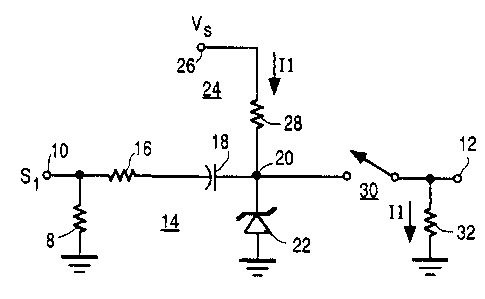
The switching apparatus of FIGURE 1 is of the cascade
type, that is, it comprises two switches connected in series
between a signal input terminal 10 and a signal output terminal
12. As previously explained, cascading switches provides
2 5 improved off-state attenuation since the attenuations of the
switches are additive.
In accordance with an aspect of the invention, the first
switch 14 of the cascade connection comprises an "L" type
attenuator having a series branch and a shunt branch. The series
3 0 branch comprises a resistor 16 and a capacitor 18 connected in
series between the signal input terminal 10 and the output node
of the attenuator. The shunt branch comprises a breakdown
semiconductor device illustrated here as being a Zener diode 22
connected at the anode thereof to a point of reference potential
3 5 (ground) and at the cathode thereof to the attenuator output
circuit node 20. Turn-on bias current for Zener diode 22 is
provided by a current source 24 comprising a supply voltage
input terminal 26 and a resistor 28 coupled between terminal 26
- 4 - RCA 85,581
and the output node 20 of attenuator 14. The second switch 30 of
the cascade connection is coupled between the attenuator output
node 20 and the signal output terminal 12 of the switching
apparatus. Turn-off bias for Zener diode 22 is provided by a load
resistor 32 coupled between signal output terminal 12 and the
source of reference potential (ground). An optional input
termination load resistor 8 may be coupled between input
terminal 10 and ground.
As a brief overview of certain features of the
switching apparatus of FIGURE 1, the attenuator 14 provides the
dual functions of ( 1 ) enhancing the over-all off-state attenuation
and (2) providing over voltage and over current protection for
input signal transients of either polarity. As discussed in detail
below the overcurrent protection or current limiting feature is
provided by resistor 16 in the series branch of the attenuator 14.
This resistor limits the input signal current for either polarity of
the input signal transient. The overvoltage protection is provided
by Zener diode 22 in the shunt branch. This breakdown device
limits the maximum positive attenuator output voltage to the
2 0 Zener breakdown value and limits the maximum negative
attenuator output voltage to the forwardbiased voltage drop of
the Zener diode. It will be appreciated that Zener diode 22 also
provides a current limiting function in that it shunts excessive
input currents to ground and by limiting the voltage to
2 5 subsequent circuits therefore also effectively limits the current to
such circuits also.
Briefly stated, control of attenuator 14 is provided by
switch 30 as follows. When switch 30 is open, all of the current of
source 24 Bows through diode 22 thereby turning the diode on
3 0 and attenuating the input signal. The precise attenuation thus
provided is discussed in detail below. When switch 30 is closed, all
of the current from source 24 is diverted through switch 30 and
load resistor 32 to ground thereby turning diode 22 off. This
reduces the attenuation to a minimum value providing a
3 5 predetermined insertion loss and also develops a predetermined
DC output voltage at terminal 12 for establishing a quiescent DC
bias for subsequent load circuitry (e.g., an amplifier, not shown)
which may be connected to output terminal 12.
- 5 - RCA 85,581 ',, ,~ ~~ ~ r~ ,~
In the specific example of FIGURE l, switch 30 of the
cascade connection is illustrated as being a single pole switch
having open and closed conditions . This switch may be of the
mechanical type i n which case the overvoltage protection
features of the invention benefit what ever utilization device (not
shown) may be connected to the signal output terminal 12 of the
switching apparatus. In a preferred application of the principles of
the invention the switch 30 would be an electronic switch which
may have plural poles and may be constructed in integrated
1 0 circuit form. FIGURE 5, discussed later, gives an example of use of
a four-position integrated circuit switch as switch 30. In that
example the benefits of over-voltage protection provided by the
present invention augment or enhance the internal over-voltage
protection that is customarily provided " on-chip" by the
integrated circuit manufacturer.
The detailed operation of the switching apparatus of
FIGURE 1 will now be discussed. When when switch 30 is in the
OPEN condition (as shown) current source 14 supplies a bias
current I 1 to Zener diode 22 which places diode 22 in a low
2 0 impedance conductive state. Capacitor 18 provides the function of
blocking the current I I in the series branch of attenuator 14. This
feature of the invention ensures that all of the Zener diode turn-
on current flows through the Zener diode 22 and none of it is
diverted to the signal input terminal 10. Advantageously, this
2 5 feature allows one to precisely determine the the operating bias
point for Zener diode 22 without regard to the impedance of the
signal source coupled to input terminal 10.
It is a feature of the arrangement that the attenuation
provided by, attenuator 14 when diode 22 is conductive may be
a
3 0 controlled by selection of the bias current I 1 and may be
determined with great precision by use of the AC equivalent
circuit of FIG. 3 in combination with the Zener diode characteristic
(conductance) curve of FIGURE 2.
In more detail, according to principles of voltage
3 5 division, the attenuation is equal to the impedance of the shunt
branch divided by the sum of the impedances of the shunt and
series branches. From the AC equivalent circuit of FIGURE 3 it is
apparent that the AC impedance of the series branch is simply the
- 6 - RCA 85,581
value of the series resistor 16 and the impedance of the shunt
branch is equal to the parallel combination of bias resistor 28 and
the on-resistance of Zener diode 22 (illustrated by a resistor 40).
One may thus readily calculate the required diode resistance for a
given desired value of attenuation and specific values of the
resistors 16 and 28. An exact equation for the diode resistance is
as follows:
R40 = K(R16)(R28) / ~ (R28) - K(R16) - K(R28) ) (1)
wherein:
R40 is the diode resistance to be determined
K is the attenuation factor expressed as a fraction,
Eo/Ei.
R 16 is the resistance of the series branch, and
R28 is the output resistance of current source 14
1 S which,
in this example is given by the value of resistor 28.
As a practical matter, the output impedance of the
current source 14 (resistor 28) may typically be quite large as
compared with the required on-resistance of diode 40. In such a
2 0 case, the equation (1) above for diode resistance simplifies to the
following:
R40 = K(R 16)/( 1 -K) (2)
Once the desired diode resistance is determined the
2 5 value of the bias current I 1 may then be determined from the
Zener diode characteristic curve of FIGURE 2. This curve (not to
scale) represents typical conductance charactistics for a low power
(e.g., one-half Watt) Zener diode having a threshold of about 6.2
volts. Threes operating points are shown. Point A represents the
3 0 diode conductance below cut-off. This operating condition is
discussed later. Points B and C represent the diode operating
points when the diode is forward biased at currents of about 1.0
and 2.5 mA, respectfully. The slope of the diode curve at a given
operating point represents the conductance of the diode. As is
3 5 seen, an increase in diode current 11 results in increased diode
conductance and thus a decrease in diode resistance.
The choice of a specific operating point (B or C)
depends on two factors, namely, the desired attenuation and the
- 7 - RCA 85,581
maximum expected negative going excursions of the input signal.
More specifically, the diode operating point (in terms of turn-on
current) should be high enough that the diode on resistance
satisfies the desired attenuation (equations 1 or 2 above) and
S that- peak negative input signal excursions do not turn the diode
off. For these reasons when switching relatively large signals (e.g.,
baseband video signals) it is preferred to bias diode 22 at a point
"C" which is relatively remote from the knee of the diode curve
rather than at point "B" which is relatively close the the knee of
the curve. Where the input signal to be switched is a small signal
(e.g., an RF signal of a few hundred millivolts) operation may be
much closer to the knee of the characteristic curve without danger
of the input signal driving the diode to cut-off.
Another consideration for the choice of a specific diode
operating point is the overall power dissipation. It will be noted
that power is dissipated in resistor 28 and diode 22 when switch
30 is open and power is also dissipated in resistor 28 and resistor
32 when switch 30 is closed. For minimum power dissipation one
would choose the lowest operating point for Zener diode 22 which
2 0 would meet the dual objectives of ( 1 ) providing addequate
attenuation and (2) providing a margin of safety to ensure that
the maximum negative value of the expected input signal does not
turn the Zener diode off during normal operation of the switching
apparatus. A further consideration concerns switching speed. It is
2 S generally faster to divert current from the Zener diode and its
associated parasitic capacitances to achieve turn-off if the current
is of a lower value. To summarize, the operating point for the
condition when Zener diode 22 is turned on depends on a number
of factors including: required attenuation, the maximum negative
3 0 value of the input signal to be switched, the overall power
dissipation and switching speed. For baseband video switching of
a nominal 1-V P-P (one volt peak to peak) video signal an
operating point of about 2.7 mini-Amperes (point C in FIG. 2) has
been found to be satisfactory for a typical 400 milk-Watt 5.6 Volt
3 5 Zener diode.
Returning to FIGURE l, when switch 30 is CLOSED the
load resistor 32 diverts the current I 1 from Zener diode 22
thereby turning diode 22 off and an input signal S 1 applied to
_ g - RCA 85,581
terminal 10 is conducted to output terminal 12. In order to ensure
that diode 22 is fully turned off one may select Il and the value of
load resistor 32 such that the product of the current Il and the
value of load resistor 32 is less than the break-down voltage of
diode 22. This may be expressed mathmetically as:
(Il)(R32) < Vz (3)
wherein: Il is the current provided current source 14:
R32 is the value of the load resistor 32;
and Vz is the threshold voltage of Zener diode 22.
Advantageously, if equation (3) is satisfied for the
switch of FIGURE 1, then it is ensured that all of the current Il will
be diverted to the load resistor 32. This follows because capacitor
18 blocks the flow of direct current in the series branch and diode
22, when off, is essentially an open circuit. Accordingly, the
quiescent DC component of voltage produced at output terminal
12 for this condition is fully independent of the series branch
impedance and is also independent of whatever DC component
may be present in the input signal applied to input terminal 10.
In more detail, in a preferred application of the
2 0 invention, the supply voltage Vs and the values of resistors 28
and 32 are selected such that the Zener diode is biased at a
potential of about 4 volts when switch 30 is closed (point A in FIG.
2). At this voltage the Zener diode 22 is completely turned off yet
the output voltage is positive with respect to ground and provides
2 5 a DC quiescent level suitable for biasing the input stage of a DC
coupled amplifier which may be coupled to output terminal 12.
This is shown and described in detail later with regard to the
discussion of FIG. 5 and provides the advantage of the possibility
of completely eliminating the need for DC bias circuits for the
3 0 following DC coupled amplifier. In other words, the bias circuitry
for the diode switch serves a dual function of also providing
proper DC bias for a following amplifier thereby providing an
economy of parts and thus improved overall reliability of the
switching and amplifying circuit.
3 5 Consideration will now be given to the insertion loss of
the switching apparatus of FIGURE 1. FIGURE 4 is an AC
equivalent. circuit of the switching apparatus for the condition
where switch 30 is closed. To simplify the analysis of the
- 9 - RCA 85,581
equivalent circuit it is assumed that the on-resistance of the
switch 30 is negligible as compared to the value of the load
resistor 32. With this assumption the attenuation of the overall
switching circuit is equal to the resistance of the shunt branch
(resistors 28 and 32 in parallel) divided by the sum of the
resistances of the series branch (resistor 16) and the shunt
branch. This may be expressed as:
A = (R28)(R32) / [ (R16)(R28)+(R16)(R32)+(R28)(R32) ] (3)
Wherein A is the attenuation Eo/Ei,
1 0 R 16 is the value of the series branch resistor,
R28 is the value of the output impedance of current
source 14 (i.e., resistor 28) and
R32 is the value of the load resistor 32.
By selecting values for the load resistor 32 and the
current source 14 impedance to be large with respect to the series
branch impedance (resistor 16) the overall insertion loss of the
switching apparatus can be made quite small. As a first example,
an insertion loss of only about 1.2 dB is obtained using the
following resistor values: R16=270 Ohms, R28=5600 Ohms and
2 0 R32=2700 Ohms. As another example, an insertion loss of less
than 3 dB is obtained when using the resistor values: R16=270
Ohms. R28=2200 Ohms and R32=1000 Ohms. This latter set of
resistor values has been used in implementing a presently
preferred embodiment of the invention shown in FIGURE 5.
2 5 FIGURE 5 presents further features of the invention
for providing switching between multiple sources and for
providing amplification of the switched signals. In this
embodiment of the invention the circuitry is simplified in that
only a singe load resistor is needed for all the sources and the
3 0 feature of providing a predetermined output voltage is used to
advantage in providing DC bias for an output direct coupled
amplifier. The amplifier completely overcomes the insertion loss
of the switch and provides additional gain as well. The advantages
which flow from the basic configuration of FIGURE 1 are thus
3 5 enhanced by improved reliability for switching multiple input
signals due to a reduction in the number of load resistors required
and a reduction in the number of parts wr~ich otherwise would be
required to establish DC bias for the amplifier.
CA 02027979 2000-12-07
RCA 85,581
-10-
In detail, the example of FIGURE 5 is designed for selecting one of
four input signals for processing by a television apparatus such as a
recorder, a
receiver, a monitor, a special effects device or the like. The four input
terminals
500-506 are each terminated by terminating resistors 508-514. For this
specific
s application, video switching, the terminating resistors are selected to be
slightly
higher than the characteristic impedance of the signal sources, an exemplary
value being 82 Ohms for a source impedance of 75 Ohms. The reason for
choosing a slightly higher terminating resistance than the source impedance is
that when the switch is turned on an additional load is presented to the input
io signal terminal. This additional load is effectively in parallel with the
input
resistor and thus reduces the effective termination impedance to the
characteristic impedance of the signal source coupled to terminals 500-506.
Attenuators 516-522 are coupled to inputs 500-506 and are of the
same construction as the attenuator 14 of FIGURE 1. Exemplary element values
15 for the attenuators are as follows:
Series resistor: 2;70 Ohms
Series capacitor;; 47 micro-Farads
Shunt Zener: 5.fi Volts, 1/2 Watt
Turn-on bias for' each of the attenuators is provided by a supply
2o voltage terminal 530 which is coupled to the output nodes 532-538 of
attenuators
516-522 by respective resistors 540-546. An exemplary value for each of these
resistors is 2200 Ohms.
The outputs 532-538 of attenuators 516-522 are connected to
respective inputs 552-558 of a four-input single throw switch 550. This switch
25 (outlined in phantom) includes four individual switches (A, B, C and D)
controlled by a decoder 560 such that one of the four switches is closed in
response to a two-bit binary control signal applied to the switch decoder
inputs
562 and 564. The outputs of the four switches A-D are connected in common
and to an output terminal 556. An integrated circuit analog multiplex switch
3 o having these features is the type CD-4052 which is available from various
manufacturers. See, for example, the DATA BOOK entitled "RCA COSMOS
Integrated Circuits" published by RCA Corporation in 1980.
CA 02027979 2000-12-07
RCA 85,581
-11-
The data book includes other switch configurations (e.g., SPSP,
DPDT and TPDT) suitable for practising the invention. Other suitable switches
are available from other manufacturers in CMOS technology and in other
integrated circuit technologies (e.g., NMOS, PMOS and bipolar).
s Advantageously., only a single load resistor 560 need be connected
to the switch 550 output terminal 556. Since all the component values of the
termination, attenuation and current sources are the same, the DC output
voltage at terminal 556 will be the same for any one of the four input signals
that
is selected, namely, 4 volts for' the specific values noted above.
to The output 556 of switch 550 is directly connected to the input 572
of a DC amplifier 570 having a supply voltage input terminal 574 connected to
supply terminal 530 and having an output terminal 576 for providing an
amplified output signal. Amplifier 570 includes an NPN input transistor 578
biased by a potential divider comprising resistors 580 and 582 connected in
i5 series in the order named between a supply terminal 572 and ground. The
collector of transistor 578 is coupled to the base of an output transistor 586
and
to the supply terminal 574 via a load resistor 584. The output transistor 586
is
connected at the emitter thereof to supply terminal 574 via an emitter load
resistor 590 and is connected at the collector thereof to output terminal 576
and
z o via a load resistor 592 to ground.
Exemplary valmes for the elements of amplifier 570 for providing a
gain of about 6 dB are as follows:
Resistor 580: 10 KOhrr~s Resistor 582: 1K KOhms
Resistor 584: 1.5 KOhrns Resistor 590: 1 KOhms
25 Resistor 592: 2 KOhms; Supply: 12 Volts
Advantageously, it will be noted that no internal DC biasing provisions
are needed for amplifier 570. 'This feature of the invention results because
the
proper DC bias for this amplifier is provided by the current source resistors
540-
546 and the load resistor 560 of the switching circuit. As previously
explained these
3 o elements provide a DC output voltage of about 4 volts for the exemplary
element
values given. Since decoder 560 turns on only one switch at a time the DC
output of
the switch 550 is the same regardless of which of the input signals is
selected. The
-12 - RCA 85,581
elimination of a separate DC bias circuit for amplifier 570 both
reduces the amplifier cost and improves its reliability since there
are fewer parts required to implement the amplifier and thus
fewer parts are subject to failure than otherwise would be the
case.
It will be further noted in the embodiment of FIGURE
5 that the amplifier supply terminal 574 and the current sources
(540-546) for the attenuators 516-522 are connected to a
common supply voltage terminal 530. By this feature of the
invention the DC bias for the amplifier 570 provided by the
attenuators and the load resistor is made to "track", so to speak,
variations in the supply voltage applied to terminal 530. Stated
another way, variations in the overall supply voltage are
compensated for since a decrease in supply voltage will decrease
1 5 both the DC output voltage across load 560 and the DC operating
potential for amplifier 570 and vice versa. This tends to maintain
amplifier 570 in a linear operating range notwithstanding
variations in the supply voltage, Vs.
In FIGURE 6 the positions of the switches are reversed,
2 0 that is, the attenuator 14 is placed after switch 30 in the cascade
connection rather than preceeding the switch 30. In this
embodiment the resistor 16 has been omitted. As will be
explained, the function formerly provided by resistor 16 of
providing a series impedance for the series branch of attenuator
2 5 14 is provided instead by switch 30 which, in the open condition,
represents a very high impedance comprising, mainly, capacitive
reactance due to parasitic coupling capacities associated with the
switch elements. Since the impedance of switch 30 when open is
very high compared with the "ON" resistance of diode 22, the
3 0 attenuation is very high also.
In more detail, in FIGURE 6 the signal input terminal
10 is coupled to ground via an input terminating resistor 8 (which
is optional, as previously explained) and is coupled via a DC
blocking capacitor 18 to the input of switch 30. The load resistor
3 5 32, previously connected at the output of switch 30 is now
connected between the input of switch 30 and ground. The
attenuator 14 output node 20 is coupled ma resistor 28 to a
supply terminal 26 for receiving the supply voltage Vs and is
-13 - RCA 85,581
coupled to the cathode of Zener diode 22 the anode of which is
grounded. A DC coupled amplifier, such as amplifier 570 of FIG. 5,
is connected at its input to the attenuator output node 20 and
connected at its output to output terminal 576.
The general operation of this example is much the same
as in the previous example of FIGURE 1 and so will be discussed only
briefly here. When switch 30 is open, the current 11 flowing through
resistor 28 turns-on Zener diode 22 thereby providing a low
impedance between the attenuator 14 output and ground. This
1 0 corresponds to the bias condition shown as points "A" or "B" in
FIGURE 2. Since switch 30 is open and the input impedance of
amplifier 570 is very large compared with the impedance of diode
22, essentially all of the I 1 current flows through diode 22 to
ground. The attenuation for this condition is given approximately by
the equation:
A = Zs / (Zd + Zs) ( 4 )
wherein: A is the attenuation, Eo/Ei;
Zs is the impedance of the series branch with switch
30 open; and
2 0 Zd is the impedance of Zener diode 22 for the
value of bias current I 1 selected.
When switch 30 is closed the current Il is diverted
through switch 30 and load resistor 32 to ground thereby turning
Zener diode 22 off. Capacitor 18 prevents diversion of the current
2 5 ~1 to the input terminal 10 or to the input termination resistor 8.
As in the previous discussion, the values of the supply voltage Vs
and resistors 28 and 32 are selected to bias Zener diode 22 at a
predetermined voltage when switch 30 is closed to thereby
provide DC .bias for the input of the amplifier 570. Resistor 16 is
3 0 not needed in this example because the impedance of switch 30
when open is quite high.
The benefits of over-voltage protection are retained in
this example of the invention to the extent that Zener diode 22
limits positive transients and negative transients appearing at the
3 5 output of switch 30 and thus protects the subsequent circuitry
(e.g., amplifier 570) from such transients.
-14 - RCA 85,581 s~ g-~ s~,
~ d :.~
The example of FIGURE 6 does not readily lend itself to
applications requiring multiple pole switching. For such
applications the example of FIGURE 1 is preferred since several
switches may be combined by connecting their outputs together
as shown in FIGURE 5.
There has been shown and described herein examples
of switching apparatus in which switches are cascaded for
improved off-state attenuation. In the embodiments shown, one
switch of the cascade connection comprises an L-type attenuator
with a series branch including an impedance and a shunt branch
including a Zener diode. In the examples of FIGURES 1 and 5 the
impedance of the series branch is provided by a resistor whereas
in the example of FIGURE 6 the impedance of the series branch is
provided by the other switch of the cascade connection. A bias
network, coupled to the attenuator and to the other switch of the
cascade connection controls the diode bias for operation at a
specific current conduction level when the other switch of the
cascade connection is open and at a specific reverse bias voltage
condition when the second switch is closed whereby the apparatus
2 0 provides plural functions, such as: ( I enhancing the switch off-
state attenuation, (2) providing over-voltage and over-current
protection for input transients of either polarity and {3) providing
a predetermined output DC level when the second switch is closed
for establishing the DC bias of a subsequent circuit, such as an
2 5 amplifier, the DC bias being so supplied being in a tracking
relationship with the DC power supplied to the subsequent circuit.