Note: Descriptions are shown in the official language in which they were submitted.
PROJECTION CATHODE RAY TUBE
BACKGROI~ND OF THE INVENIION
Field of the Invention~
This invention relates to a projection cathode ray tube in which an image on
a phosphor layer is enlarged and projected on a screen located at a given distance
ahead through a projection lens unit in front of the phosphor layer. -
~ . ` ~,.'
Descril7tion of the Related Art:
United States Patent No. 4,642,695 (Vriens et al) discloses an example of
improving the efficiency of focusing the luminous flux into the projection lens unit
from each of the monochromatic cathode ray tubes.
In a conventional cathode ray tube, light emitted from the phosphor screen is ~
in a state of highly close to, what is called, a completely scattered light. In a ~:
projection television apparatus, only the luminous flux emitted from the phosphor
screen within the divergent angle of 30 is utilized, while the remaining luminous
flux is lost. According to the above-disclosed example, the brightness of image on ;
a screen of the projection television is greatly enhanced by converging 30% or more ~i
of the entire luminous flux emitted from the elements of the light-emitting phosphor
screen into a cone-shaped area having the divergent angles within -30 to 30.
Further, Japanese Laid~pen Patent Application No. 61-273837 (Rehindelt
Prience et al) discloses a projection type cathode ray tube having a multilayered
interference filter composed of alternately superimposed layers of high refractive
index material and low refractive index material disposed between the inner surface
of the face plate pane of the cathode ray tube and the innermost luminescent material
layer provided in the cathode ray tube, for example. As examples of structural
components, tantalum pentoxide ~a2O5) or titanium dioxide ~iO2) is used as high
refractive index material whereas silicon dioxide (SiO2) or magnesium fluoride
(MgF2) is used as low refractive index material. In general, the multilayered
interference film is formed of layers of low refractive index material layers and high
refractive index material alternately superimposed up to six layers or more.
i -
In a projection cathode ray tube having a conventional multilayered
interference film disposed upon the inner surface of the face plate pane, the optical
thickness nd (where n is the refraction index and d the thickness) of each layer of the
multilayered interference film is between 0.2 and 0.3 Af in a~cordance with the
S example disclosed in Japanese Laid-open Patent App~cation No. 61-273837.
Specifica11y, according to this example, the projection cathode ray tube comprises a
multilayered interference film composed of six or more layers, the optical thickness
nd of which is within 0.23 to 0.25 'Af, namely, around ~f /4. Here the followingequation is obtained.
'Af = p X ~
where ~ denotes a desired central wavelength selected from the emission spectrum of
the luminescent material; p, a value in the range from 1.18 to 1.32. As another
example, Japanese Laid-open Patent Application No. 61-39349 (Rehindelt Frience et
al) di~closes a projection cathode ray tube having a mul~layered interference film
composed of approximately 14 to 30 superimposed layers, the optical thickness ofwhich is almost as same as that of the aforementioned example. ;
During the manufacturing process, a cathode ray tube typically undergoes
three heat processing steps, the temperature of which is within about 350C to
450C, such as baking, frit sealing and exhaust steps. In view of the heat processing,
before passing through the above-described manufacturing steps, the cathode ray tubes
have previously bsen processed by baking at a temperature ranging from 450C to ~ ~-
500C so as to s*cure the multilayered interference film which has been deposited by
the evaporation. ;;
However, in the existing multilayered interference film mentioned above, the
number of layers comprised becomes considerable, for example, it amounts to six or
more layers, sometimes up to 14 to 30 layers. This is disadvantageous in that ~;;
because of the differences in the thermal expansion coefficients between the high
refractive index material and the low refractive index material of the multilayered
interference film, a thermal distortion occurs at each layer of the multilayeredinterference film due to the aforementioned heat processing, thereby causing cracks ~ ~
or afilm separation. ; ~;
- 3 -
SUMMARY OF THE INVENTION -
This invention aims to solve the above-described drawbacks of the
conventional cathode ray tubes, and the purpose of the present invention is to provide
a projection cathode ray tube equipped with a multi1ayered interference film which
S is not subject to the cracks or film separation due to the heat processing. According
to one aspect of the present invention, there is provided a projection cathode ray tube
comprising: a face plate pane; a luminescent material layer; and a multilayered
interference film disposed on the inner surface of the face plate pane between the
luminescent material layer and the face plate pane, the multilayered interference film -
10 comprising four altemately superimposed layers of high refractive index material and
low refractive index material and the optical thickness of each layer of the
multilayered interference film is ~ /4, wherein ~ + ~p, ~ is a central
wavelength selected from the luminous spectrum of said luminescen~ material and ~p
has a value between 20nm and l00nm.
A projection cathode ray tube according to this invention is provided with
light-emifflng phosphors activated with terbium ~b); the layer of high refractive
index material comprises tantalum pentoxide ~a205); and the layer of low refractive
index material comprises silicon dioxide (SiO2).
PracticaUy, the optical thickness of each layer of the multilayered interference20 film is set to ~h /4. Here, ~ /4 is expressed as ~ p, where )~h is a
wavelength at which the transmittivity is 50% ~ denotes a central wavelength selected
from ~e emission s~ectrum of the luminescent material, and ~p is a value between20 nm and l00 nm.
With this asrangement, it is possible to obtain a sufficient efficiency of
25 focusing the luminous flux emitted from the phosphor screen (luminescent material
layer) into the projection lens unit positioned in front of the cathode ray tube, by use
of a reduced number of interference layers, thereby reducing the risk of cracks or
film separation due to the heat processing.
The above and other advantages, features and objects of this invention wiU be
30 apparent to those skilled in the art upon making reference to the foUowing detailed
description and the accompanying drawings in which several structural embodiments
~. ~ ;
:
-4-
incorporating the principles of this invention are shown by way of illustrative
examples.
BRIEF DESCRIPlION OF TEIEDRAVV~IGS
S FIG. 1 is a fragmentary sectional view illustrating a face plate pane of a
projection cathode ray tube in accordance with one embodiment of the present
invention; ;~
FIG. 2 is a flow diagram illustrating manufacturing processes of a projection
cathode ray tube comprising a multilayered interference film;
EIG. 3 is a spectral transmittance - wavelength characteristic showing a
transmiffivity of a multilayered interference film;
l~IG. 4 is a spectral transmittance - wavelength characteristic illustrating thetransmiffivity of a multilayered interference film which varies in response to the ~ `
number of layers. ` ``
;-
DETAILED DESCRIPIION OF THE PRE~RR~ EMBODIM~TS
A projection cathode ray tube in accordance with a first embodiment of the - ~present invention will now be described hereinbelow. - ~'`,
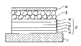
Fig. 1 is a fragmentary section view illustrating a face plate pane of a
projection cathode ray tube incorporating a multilayered interference film in
accordance with a first embodiment of the present invention.
Fig. 1, reference numeral 1 designates the face plate pane; 2, the multilayered `
interference film; 3, luminescent material layer; 4, an aluminum evaporation film for ,
reflecting the light emitted by the phosphor screen which is scattered in the direction
opposite to the face plate pane 1, out of the cathode ray tube, ;
In a first experimentally fabricated cathode ray tube in accordance with a first ~ ~ `
embodiment of the present invention, there is obtained a projection cathode ray tube :
equipped with a multilayered interference film comprising five layas, e~ch of which
has an optical thickness of ~ /4. Layers of high refractive index material made up
of tantalum pentoxide ~a2Os) are alternately superimposed with layers of low
refractive index material made up of silicon dioxide (SiO2). The multilayered
intaference film has a wavelength of )~" = 615 nm while the green-luminescent
B ` ~
phosphor screen, which is activated with terbium ~rb), has the wavelength ~ within
SM nm to 545 nm. Here, the following equation is established.
~ = ~p + ~
where ~h denotes a wavelength where the transmittivity becomes 50% on the optical
S transmifflvity spectral characteristic of the multilayered interference film shown in
Fig. 3; ~, a desired central wavelength selected ~om the light-emitting spectrum of
the luminescent material; and ~p a value between 20 nm and 100 nm. When the
cathode ray tube was fabricated experimentally, no separation of the multilayered
interference film occurred. Such separation frequently occurs in the conventional
10 manufacturing processes even when the cathode ray tube has repeatedly been
processed through the heat processing steps.
Furthermore, regarding the optical characteristics, it was confinned that the
brightness is enhanced by about from 150% to 170% in the direction of optical
normal of the face plate pane in comparison with the cathode ray tube without the
15 multilayered interference film. Moreover, owing to the filter characte~istics of the
multilayered interference film, the colour tone and contrast of the image are
improved.
In the multilayered interference film, the cutoff wavelength of the optical
transmittance characteristics is detenl~ined by the optical thickness nd of each layer
20 Here, the reference symbols n and d express the refraction index and the thickness
respectively. Also, the number of the superimposed layers defines the effectiveness
of the fllter characteristics with respect t~ the optical transmittance characteristics.
Regarding the number of layers included in the multilayered interference film,
Japanese Laid-open Patent Application No. 61-39349 describes that when the number
25 of the layers is smaU, the angle, or the acceptance angle at which the magnitude of
reflected luminous flux is extremely reduced, is not smaU enough and it becomes
difficult to obtain sufficient luminous flux focuseid on the projection lens unit. To
specify the position of the edge of the multilayered interference film at which the
transmittivity varies, namely, to precisely specify ~f in the equation ~f = p)~ and to
30 reduce the acceptance angle, it is neressary to provide a large number of layers in the
cathode ray tube. To this end, Japanese Laid-open Patent Application No. 61-39349
,
.
13. : `
- 6-
discussed that the multi-layered interferencei should preferably bei made of
substantially 14 to 30 layers.
Likewise, Japanese Laid-open Patent Application No. 61-273837 discloses the
transn~ittance ~haracteristics obtained by multilayered interference filters of six or
S more layers. The transmittance charactenstics obtained respectively with a filter of
14 layers and with a film of 30 layers are disclosed in the above-mentioned
application.
In production, however, the bigger the number of layers to be superimposed
is the larger becomes the thermal deformation which occurs at ea~h layer due to the
10 heat processing. As well the multilayered interference film is more frequently liable
to cracks and film separa~on.
Tn the first embodiment of the present invention, since the multilayered
interference film comprises five layers, the problems disclosed in aforementioned
Japanese Laid-open Patent Application No. 61-39349 (that is, the acce~tance angle
15 being too large) remains unsolved. ~Iowever, when the cutoff wavelength is properly
selected, the loss of the luminous flux is extensively reduced in the direction of the
normal of the multilayered interference film, namely, in the direction in which the
. ~:
luminous flux is emitted in palallel with the normal. As a result, there is obtained
a projection cathode ray tube having a multilayered interference film which is not
~ , . ..
subjectto cracks and film separation.
In Fig. 4, a reference A designates a transmission wavelength area; B, a
; , ~ .
transition area at which the transmittance characteristics may change from the
transmission wavelength area to the nontransmission wavelength area; C, a
nontransmission wavelength area or a low transmission wavelength area. The dashed
line I represents the t~nsmittance cha~cteristics of a m~ti~yered interference film
consisting of 4 or 5 layers in accordance with the present invention, and the solid ~e
11 represents the transmission ch~cteristics of a conventional multilayered
interference f~m consisting of ten or more ~yers. ,
Selecting a proper cutoff wavelength means that it is ne~issary to select ~ in ~ `~
the longer wavelength domain. According to the transmifflvity c~ve of the luminous -
flux shown in Fig. 4 when the number of layers constituting the inte~erence ~m
decreases, the inclination of the slope at which the transmiffivity declines is gentler r
.,:' .: '
'~t : ", ' :
'i~ .! '' ~' ''
r;, ' ~ ~, "'' . .. , . ':
.: . '
.. ..
(area B of Fig. 4) and the value of transmifflvity in the wavelength domain where the
transmittivity is generally small increases, (area C of Fig. 4). Particularly, as
mentioned for this embodiment, it is preferable to set the )~p to values within 20 nm
to 100 nm under the equation of )~ p + )~-
S Second and third experimental embodiments of the present invention will now
be explained.
As a result of the experimental fabrication of a second embodiment of the
cathode ray tube of the present invention, a projection cathode ray tube comprising
a multilayered interference film composed of four layers was obtained. The film
comprised alternatively superimposed layers of tantalumpentoxide (Ta2O5) and silicon
dioxide (SiO2), having a ~h of 520 nm, and a layer optical thickness of ~h /4. The
luminescent material layer is of blue phosphors which are formed of zinc sulfide, is
activated with silver, and has a ~ of 450 nm.
In the second experimental embodiment, like the first experimental
embodiment, no cracks and film s~paration which frequently occur with the
conventionat structure have been observed after the film was manufactured passing
through the heat processing steps several times. Regarding the optical characteristics,
the brightness has been enhanced by about 140% to 150% in the direction of the
normal of the face plate pane compared with the projection cathode ray tube having
no multilayered interference film. Moreover, the colour tone and contrast of thesecond experimental cathode ray tube are improved in the same manner as that
attained by the first experimentally fabricated cathode ray tube.
In the third experimental embodiment of the projection cathode ray tube
comprised five layers of alternately superimposed titanium dioxide (TiO2) and silicon
dioxide (SiO2) having a centrat wavelength of 615 nm and a layer optical thickness
of ~b /4. The luminescent material layer comprises green phosphors activated with
terbium ~b) and has a ~ of 544 to 545 nm.
In this third experimental embodiment, like in the first one similar results areobtained in respect of the cracks, the film separation, and the optical characteristics.
Although the explanation is merely given to the embodiments uti1izing
tantalum pentoxide ~a205) or titanium dioxide (TiO2) for a high refractive indexmaterial and silicon dioxide (SiO2) for a low refractive index material, through the
- 8-
experiments it is confirmed that with the structure in which the interference film
comprises 4 or 5 layers it is possible to obtain projection cathode ray tubes having a
multilayered interference film which is not subject to cracks and film separation after
having completed the heat processing for securing the multilayered interference film
5 or the heat processing performed several times in the manufacturing process of the
cathode ray tube, even when other materials are employed for the components of the
interference film instead of the above-mentioned materia1s. Such alternative materia1s
can be niobium pentoxide (Nb205) or zinc sulfide (ZnS) for a high refractive index
material and magnesium fluoride for a low refractive index materia1.
As another embodiment of the present invention, although ~e explanation is
given to the green and blue luminescent materia1s, the same structure is applicable to
the red phosphors of yttrium oxide (Y203) activated with europium (liu).
It has been found that it is impossible to obtain the desired optical
characteristics with an interference film having three layers or more, and therefore,
lS a cathode ray tube having such structure is not suitable for practical use.
As described above, in accordance with the present invention, with respect to
the projection cathode ray tube comprising a phosphor screen formed of a luminescent
materiat layer disposed upon the inner surface of a face plate pane and a multilzyered
interference fitm disposed between the phosphor screen and the face plate pane and
20 composed of a plurality of layers alternately superimposed of a high refractive index
materiat and a low refractive index materiat, since the number of the muttilayered
interference layers to be superimposed is limited to four or five layers, the brightness
is highly improved in the direction of the normat of the face plate pane, thereby
making it possible to obtain the projection cathode ray tube the multilayered
25 interference film of which is not subject to the crack~ and film separation after
passing through the severat heat processing steps in the manufacturing processes.
: ,:
~'.' ;;',''.'".' ."
i. ' ,.-...
, ',. '' ' ,:
'' ,' ~ '', :
- : ~
.': ~ ' '