Note: Descriptions are shown in the official language in which they were submitted.
2028328
The present invention relates to an optical device
in optical communication systems more particularly, to a
single directional optical divider with low loss for
distributing an input light to a plurality of optical
systems by employing an optical waveguide.
An optical divider is an important device for use
in distributing an input light to a plurality of optical
systems in optical communication systems or optical data
link systems, and there are several types of optical
dividers such as a micro-optics type, a fused fiber type and
an optical waveguide type. Above all, an optical divider of
the optical waveguide type has excellent properties such
that full of flexibility in designing, easy to obtain multi-
branching circuits, suitable for mass-production and so
forth. Accordingly, it has been studied for making
practical use of such optical dividers and various
propositions have been made heretofore.
An optical divider which employs a thick film
optical waveguide for use in multimode fiber systems has
such a structure wherein an input optical fiber and a
plurality of output optical fibers are closely coupled to
the opposite ends of a light transmissible substrate, in
which substrate an optical waveguide is formed by a
technique of photolithography or the like, so that the light
entering from the input optical fiber is distributed and
coupled to the plurality of output optical fibers by means
of the optical waveguide. More practically, the light
transmissible substrate has a further reinforced structure
and is connected and secured by utilizing a bonding agent,
which also acts as a refractive-index matching member, to a
fiber array composed of optical fibers being aligned and
secured to each other.
~;;
2028328
One of the most important properties of an optical
divider produced in this manner is an optical loss, and it
is a very important subject for the practical use of an
optical device how to reduce the optical loss.
The optical loss is divided roughly into two types
of losses, one of which is a transmission loss encountered
in transmitting a light signal through an optical waveguide
and the other of which is a coupling loss to be caused when
coupling an optical fiber to the optical waveguide. The
coupling loss is further divided into two types of losses,
one of which is a shape loss derived from the difference in
cross sectional shapes between the optical waveguide and the
optical fiber core and the other of which is a loss derived
from mismatching of numerical apertures (N.A.) between the
optical waveguide and the optical fiber.
Accordingly, in order to fabricate the optical
divider having low optic ~
~2
2028328
check every factor relating to the losses and reduce
them as much as possible.
The transmission loss depends on a material of
which the optical waveguide is made and a method of
fabricating the optical waveguide, however, these are
not called in question herein.
The shape loss is derived from the difference in
cross sectional shapes such as when the optical fiber
core is of circular cross section while the optical
waveguide is of other than the circular cross section.
Besides an optical waveguide fabricated by an ion migra-
tion method for multi-component glass through diffusion
process (~. Okud~ et al., Appl. Opt., 23, 1745, (1984)),
such an optical waveguide as a quartz glass waveguide
fabricated by a flame deposition method (Y. Yamada et
al., Electron Lett., 20, 313 (1984)) or a high polymer
waveguide fabricated by a selective photopolymerization
method (T. Kurokawa et al., Appl. Opt., 19, 3124 (1980))
has a substantially rectangular cross section, and
thereby causing optical losses at a coupling portion
with the optical fiber having a circular cross sectional
core. For example, a 4-port branched circuit which
includes a connection of 2-port branched circuits in
which each core has an equal width is shown in FIG. 2A.
Where such contrivance is made in circuit con-
struction upon designing a circuit, so far as it is used
as an optical divider, if an optical waveguide is formed
2028328
into the same circular shape as that of the optical fiber,
an optical divider having no optical loss my be provided
ideally (if it is used as a mixer in the opposite direction,
inherent loss of 3 dB may take place at each of mixing
parts). However, if an optical waveguide has a rectangular
cross section, a coupling portion of the optical waveguide
against an optical fiber derives a coupling loss from places
where the input light from the input optical fiber is not
received by the optical waveguide core. While, at the
output side, the output light from the optical waveguide
core is not received by an output optical fiber, thus
resulting in the coupling loss.
In such circuit structure, it is known that the
overall coupling losses at the input side and the output
side can be minimized by optimizing the thickness and width
of the optical waveguide (T. Kurokawa et al., Appl. Opt.,
19, 3~24 (1980)). In the case of Step-index (SI) optical
fibers, the minimum shape loss of 0.8 dB is achieved by
shaping the optical waveguide into such that a side of the
cross section of which equals to 90% of a core diameter of
the optical fiber to be connected.
If an optical divider is formed into a circuit
structure by making use of properties that can be used for
a single directional transmission of light signal, it is
possible to reduce the shape loss. That is, if the optical
divider is fabricated in such a manner as to form an optical
circuit which is composed of a main optical waveguide for
being coupled to an input optical fiber and branching
optical waveguides having contiguity to the main optical
waveguide for being coupled to a plurality of output optical
,~ .
2028328
fibers, it is possible to make, at the input side, the width
of the optical waveguide sufficiently wider than a core
diameter of the input optical fiber at the input side and
that, at the output side, the width of the optical waveguide
sufficiently narrower than a core diameter of the output
optical fiber to be connected. With this circuit
arrangement, the shape loss to be caused in the optical
circuit can be eliminated substantially.
While such circuit structure has some
disadvantages such that, particularly when branching
waveguides are great in number, the width of the main
optical waveguide becomes wide correspondingly and results
in a change for the worse in loss variance. However, such
defect may be improved or eliminated by selecting the length
lS of the main optical waveguide as well as the widths of
branched optical waveguides suitably.
As described in detail above, while the shape loss
in the coupling loss of the optical divider can be reduced
significantly by selecting a suitable circuit structure,
however, the loss derived from the mismatching of numerical
apertures between the optical waveguide and the optical
fibers still remains.
The numerical aperture N.A. of each light
transmissible medium is given by a sine of the angle of
emission (or the angle of incidence) N.A. = sin~ from its
definition. The actual coupling loss derived from the
mismatching of the numerical apertures between the optical
fiber and the optical waveguide is given by the following
formula:
Coupling loss (dB) = [10 log(N.A.wG/N.A. fiber) ] (1)
2028328
where, N.A. WG is a numerical aperture of the optical wave-
guide, whereby a geometric mean value is used when the
numerical aperture differs in a lateral direction and a
vertical direction of the film as in a case that
5~
~f
_=
2~2~328 - ~
the optical waveguide is fabricated by a selective
photopolymeri~ation method, and N.A. fiber iS a numerical
aperture of the optical fiber.
As it is apparent from the formula (1), the loss
derived from the mismatching of the numerical apertures
becomes zero when the numeric~l aperture of the optical
waveguide coincides with that of the optical fiber. On
the other hand, when refractive-indices of a core and
clad of the optical fiber are designated by nc~re and
nclad~ respectively, the numerical aperture N.A. is
related to those indices in accordance with:
N.A. = (ncore- nclad)l/2 (2)
accordingly, it can be seen that, in order to achieve
the matching of the numerical apertures N.A., the re-
fractive-indices of the core and clad of the optical
waveguide must be controlled accurately. However, the
control of the refractive-indices is not always easy.
If it is assumed that the numerical aperture of the
optical waveguide which has actually fabricated is 5 %
smaller than that of the optical fiber, a coupling loss
of 0.45 dB may be caused at the input side in accordance
with the formula (~). In view of the control accuracy
of the refractive-index, in a conventional method of
fabricating an optical waveguide, the accuracy of 5 %
for the numerical aperture N.A. is proximate to the
control unit and there caused is a loss of 0.5 dB or so
in times, thus resulting in a deterioration of optical
2028328
properties of the optical divider.
It is therefore an object o~ the present invention
is to provide an optical divider being reduced in coupling
loss to be derived from the mismatching of numerical
apertures and having a low optical loss.
After making an earnest examination and efforts to
reduce the coupling loss being derived from the mismatching
of numerical apertures N.A. of an optical divider and an
optical fiber and the optical loss of the op-tical divider,
lo it has been found that the coupling loss due to the
mismatching of the numerical apertures N.A. can be reduced
considerably if either the main optical waveguide or the
branching optical waveguides of an optical circuit has such
an optical waveguide structure wherein the optical waveguide
is tapered in such a way as it e~pands towards the output
side.
According to the present invention, there is
therefore provided an optical divider including an input
optical fiber closely contacted and jointed to one end of a
flat light transmissible plate member in which an optical
waveguide is formed and a plurality of output optical fibers
closely contacted and jointed to the other end thereof for
distributing input light from to said plurality of output
optical fibers, characterized in that:
- said optical waveguide has such a tapered
structure that expands towards an output side and is formed
of a main waveguide portion coupled with said input optical
fiber and branching optical waveguide portions contiguous to
said main optical waveguide portion and coupled to said
plurality of output optical fibers;
. ~
2028328
- said optical waveguide is formed to fulfill the
following conditions when a core diameter and a numerical
aperture of said input and output optical fibers are
represented by D and N.A. respectively,
(1) a width of a portion of said main optical
waveguide where is coupled with said input optical fiber is
greater than D while each width of portions of said
branching optical waveguide where are coupled with said
output optical fibers is smaller than 0.85 'D, and
(2) the range of the taper angle ~ of the optical
waveguide is given by:
2 x 10 4 < ~ (rad) < (sin ~ N.A.)/4.
Preferred embodiments will now be described as
examples without limitative manner having reference the
attached drawings, wherein:
Fig. 1 is a perspective view of an optical divider
produced by a selective photopolymerization method;
Fig. 2A is a plan view of an optical divider
showing a branched circuit composed of optical waveguides
with constant width and a state of connecting portion
between optical waveguides and optical fibers;
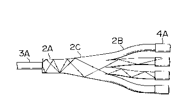
Fig. 2B is a plan view of an optical divider
showing a branched circuit composed of optical waveguides
divided equally from a main optical waveguide and a state of
connecting portion between the optical waveguides and the
optical fibers;
Fig. 3 is a schematic diagram showing the
relationship between the transmission and reception of light
whereby two media having different numerical apertures are
connected to each other;
~028~8
Fig. 4A is a plan view of a principal circuit
construction of the present invention showing a circuit
construction provided with a taper at the main optical
waveguide;
Fig 4B is a circuit construction provided with a
taper at each of the branching optical waveguides;
Fig. 5 is a principle diagram showing paths of
light beams passing through a tapered portion of the optical
divider; and
Fig. 6 is a diagram showing the reduction of
excessive loss when a taper angle is varied in a 4-port
branching circuit embodying the present invention.
An optical divider which employs a thick film
optical waveguide for use in multimore fiber systems has
such a structure as shown in Fig. 1 wherein an input optical
fiber 3 and a plurality of output optical fibers 4 are
closely coupled to the opposite ends of a light
transmissible substrate 1, in which substrate 1 an optical
waveguide 2 i6 formed by a technique of photolithography or
the li~e, so that the light entering from the input optical t,
fiber 3 is distributed and coupled to the plurality of
output optical fibers 4 by means of the optical waveguide 2.
More practically, the light transmissible substrate 1 has a
further reinforced structure 6 and is connected and secured
by utilizing a bonding agent 7, which also acts as a
refractive-index matching member, to a fiber array 5
composed of optical fibers being aligned and secured to each
other.
2028328
one of the most important properties of an optical
divider produced in this manner is an optical loss, and it
is a very important subject for the practical use of an
optical device how to reduce the optical loss.
Fig. 2A shows an optical waveguide which has a
rectangular cross section. A coupling portion of the opti-
cal waveguide against an optical fiber derives the coupling
loss from each of hatched portions of Fig. 2A at where the
input light from the input optical fiber core 3A is not
received by the optical waveguide core 2. While, at the
output side, the output light from the optical waveguide
core 2 shown by hatching in Fig. 2A is not received by an
output optical fiber 4A, thus resulting in the coupling
loss.
If an optical divider is formed into a circuit
structure such as shown in Fig., 2B by making use of
properties that can be used for a single directional
transmission of light signal, it is possible to reduce the
shape loss. That is, if the optical divider is fabricated
in such a manner as to form an optical circuit which is
composed of a main optical waveguide 2A for being coupled to
an input optical fiber 3 and branching optical waveguide 2B
having contiguity to the main optical waveguide 2A for being
coupled to a plurality of output optical fibers 4, it is
possible to make, at the input side, -the width of the
optical waveguide sufficiently wider than a core diameter of
the input optical fiber at the input side and that, at the
output side, the width of the optical waveguide sufficiently
narrower than a core diameter of the output optical fiber to
be connected. With this circuit arrangement, the shape loss
lOa
2028328
to be caused in the optical circuit structure shown in Fig.
2A can be eliminated substantially.
In Fig. 3, there is shown that how the coupling
loss is derived due to mismatching of numerical apertures
N.A., wherein an angle of emission from a core 8A of a light
transmissible medium 8 is represented by ~1 and an angle of
incidence to another light transmissible medium 9 coupled to
the light transmissible medium 8 is represented by ~2. In
the case of ~1 > ~2, lights between the hatched portions of
Fig. 3 can not be received by the light transmissible medium
9, thus resulting in a radiation mode and causing a coupling
loss.
On the contrary, in the case of ~1 > ~1, all
incident lights remain within the angle of incidence, this
results in no coupling loss.
Fig. 4A is an embodiment of the present invention
showing an optical divider (1 x 4 divider). While various
techniques are available for making an optical waveguide 2
within a light transmissible substrate 1, a selective photo-
polymerization method was employed herein (Japanese PatentPublication no. 56-3522). In particular, a film of desired
thickness containing a polycarbonate resin ("Iupilon Z", a
trade name of a product by "Mitsubishi Gas Kagaku Kabushiki
Kaisha") synthesized
~
10b
2~28328
~rom Bisphenol-Z, methyl acrylate which is a monomer
having a low refractive-index, an optical sensitizer and
some others is produced by a solvent cast method. The
film is then exposed to ultra-violet rays through a
photomask carrying a printed circuit pattern for poly-
merizing the monomer in exposed portions other than the
printed circuit pattern to form an optical waveguide
therein. It is noted that, since the effect of the
present invention is materialized by providing a flat
optical waveguide with a taper in width, it does not
rely upon a method of ~abricating the optical waveguide,
and the present invention can be embodied similarly by
employing any other method of fabricating the optical
waveguide other than the method employed herein.
In order to define the structure of the taper, it
is necessary to designate three parameters including a
circuit width Wl at a portion where the taper starts,
another circuit width W2 at another portion where the
taper ends and thereby a taper angle is ~. While it is
possible to reduce the shape loss by providing the
dividing circuit with the main optical waveguide and
branching optical waveguides as described in detail
hereinabove, however, it is necessary for the optical
waveguide that an increase of the shape loss should not
be introduced by the tapered portion. The ranges of the
widths Wl and W2 are defined in view of the above con-
sideration.
2028~28
Firstly, after various examinations have been made
as to the relationship between the width of the optical
waveguide and the coupling loss with regard to the shape
loss at the output side between the optical waveguide
and the output optical fiber, it was found that the
shape loss can be reduced substantially to zero by
making the width of the optical waveguide at or less
than 86 %, desirably 80 %, of a core diameter D of the
optical fiber. Since the optical waveguide provided by
the selective photopolymerization method employed or the
flame deposition method has a distribution of refrac-
tive-index which is close to that of a step-index (SI)
type, and thereby if the output optical fibers are of
graded-index (GI) type, the shape loss may become sub-
stantially little greater than that of SI type. Howev-
er, if the width of the optical waveguide is arranged to
be at or less than 80 % of the core diameter of the
optical fiber, the shape loss can be neglected regard-
less of ~he index type (GI or SI) of the output optical
fiber.
Secondly, at the input side, if the width of the
optical waveguide is arranged to be greater than the
core diameter of the optical fiber, the shape loss can
be reduced to zero.
The two arrangements as described above are the
essential requirements for the present invention in
order to obtain an optical circuit which is free from
2028328
the shape losses both at the input side and the output
side of the optical waveguide. The lower limit of the
width Wland the upper limit of the width W2 are deter-
mined from the condition as described above. In an N-
port optical divider, generally, the width Wl is WI > D,
while the W2 is W2 < 0.85 DN.
The optical losses have been measured with various
optical circuits by varying the taper angle ~ (or a
taper length L) to various values while maintaining
dimensions of Wl = ~0 ~m, W2 = 100 ~m, and the film
thickness = 40 ~m under use of the optical fiber 3
having 50/125GI (N.A. = 0.20). In FIG. 6, it is shown
how an excess loss is improved by providing a taper for
the optical waveguide as compared with that of the
optical waveguide, as a standard, with no taper (~ =
0). The effect of the taper is indic~ted from the
proximity of a point where the taper angle exceeds 10-4
(rad), and a constant improvement of 0.4 dB is attained
from the proximity of a point of 4 x 10⁻⁴ ( rad) through
the proximity of a point of 10-2(rad). The effect of
the taper angle can not be seen beyond the point of
-2 .
By taking into consideration of the fact that the
effective reduction of the numerical aperture is caused
by reflections at the tapered portion of the optical
waveguide, a taper angle greater than an angle of inci-
dence determined by the numerical aperture N.A. of the
2028328
input optical fiber is considered to be of insignifi-
cance, while, if the taper angle is too small, a length
of the tapered portion becomes too long, increasing a
transmission loss, thus resulting in cancellation of the
effect of the taper. A range of the taper angle within
which the tapering is effective is obtained from FIG. 6
as:
2 ~ 10-4< ~ (rad) < 4 x 10⁻² (3)
Since the upper limit is varied in response to a
numerical aperture of an optical fiber in use, the
formula (3) may be given more commonly by:
2 x 10⁻⁴< ~ < (sin~1NA)/4 (4)
Also, in the case of the circuit construction of
FIG. 4B wherein the taper is provided for each of
branching waveguides, the formula (4) stands quite
similarly if an apparent taper angle ~ is defined by
the formula (5):
~ = tan~l(W2 - W1 / 2L) (5)
According to the present invention, the coupling
loss derived from the mismatching in numerical aperture
can be reduced irrespective of the accuracy of numerical
aperture control in fabricating an optical waveguide.
As it has been described above, according to the
present invention, the coupling loss to be derived from
the mismatching of numerical apertures between the
optical waveguide and the optical fibers can be reduced
considerably by merely changing the optical circuit
14
2028328
structure in such a way as to be composed of a main
optical waveguide and branching waveguides and making it
a tapered structure. Accordingly, the optical divider
of reduced losses can readily be fabricated even if
there were variations in the production of optical
waveguides.
Although the present invention has been described
in detail with re~erence to the presently-preferred
embodiments, it should be understood by those of ordi-
nary skilled in the art that various modifications can
be made without departing from the spirit and scope of
the invention. Accordingly, the invention is not to be
limited except as by the appended claims.