Note: Descriptions are shown in the official language in which they were submitted.
~ 'J ~; 3~,
RADAR SYSTEM
Background of the Invention
This invention relates generally to radar sysltems
and more particularly to switching circuitry used as pulse
modulators for radar systems adapted to produce transmitted
pulses with different, or staggered, pulse repetition inter-
vals.
As is known in the art, it is sometimes desirable, as in
radar systems, to produce amplified pulses of radio frequency
energy. As is also known in the art, in moving target indicator
(MTI) radar systems, radar returns produced by reflections of
the transmitted pulses from objects are converted into video
signals by a phase detector. The video signals are then fed
to a canceller. Returns from stationary objects are converted
by the phase detector into video signals having the same
phase from return to return whereas returns from moving
objects are converted into video signals having a different
phase from return to return. The rate of change in such
phase is related to the velocity of the ~object. As is known
in the art, it~is typically desirable to produce a train of
transmitted radio frequency pulses having a staggered pulse
repetition interval (PRI) in order to remove velocity blind
spo~s. More particularly, as described in my chapter 17 "MTI
Radar" of Radar Handbook, Editor-In-Chief Merrill I. Skolnick,
McGraw-Hill ~ook Company, New York, 1970, ssction 17.10
~3~
beginning at page 17-38, I point out that the interval between
radar pulses may be changed to shift the target velocities to
which the MTI radar system is blind. As I pointed out in
such chapter, the interval may be changed on eithér a scan-
~5 to-scan or pulse-to-pulse basis. Further, as I describe in
section 17.13 beginning at page 17-46 instabilities come
from, inter alia, the pulse-to-pulse phase change, if a power
amplifier is used, and pulse-to-pulse frequency change, if a
power oscillator is used, thereby limiting MTI performance
because such phase or frequency changes produce changes in
the phase of the video signals produced by the phase detector.
As pointed out therein, if the phases of consecutive received
pulses, relative to the phase of the coherent oscillator
(COHO) in the receiver, differs by say 0.01 radian a limitation
of -40 db is placed on the target-to-clutter improvement
possible. The 0.01 radian clutter-vector change is equivalent
to a target vector 40 db weaker than the clutter superimposed
on the clutter. In a pulsed oscillator system, pulse-to-
pulse frequency changes result in phase runout during the
transmitted pulses. A phase runout of 0.02 radians during
the transmitted pulse would then place an average limitation
of 40 db on the improvement factor attainable.
Phase or frequency stability, as measured by so called
~pushing figures," for various RF tubes is presented in Table
6 of section 7.10 of Chapter 7, "Transmitters" of the above
.
y~f h ~J ;f~ o ~
~;
referenced Radar Handbook beginning at page 7-64. As pointed
out, the especially difficult requirement from the transmitter
standpoint is the use of nonuniform interpulse periods, usually
called staggered-PRF MTI. That is, when a power amplifier is
used, a signal produced by a continuously running radio fre-
quency oscillator is fed to the amplifier and each time a
pulse of radio frequency energy is to be transmited a control
voltage is fed to the amplifier to place it in a conduction
condition. The phase shift provided by the amplifier is a
function of the level of the control voltage. In the case of
a power oscillator, a pulse of radio frequency energy is
produced by the oscillator in response to a control voltage.
The frequency of the radio frequency energy is a function of
the level of the control voltage. The most significant source
of variation in the level of the control voltage during
staggered PRF operation is the variation in high voltage power
supply (HVPS) voltage from pulse-to-pulse that results from
the nonuniform power drain on the HVPS. As noted, even if
the HVPS voltage is held constant, variations in the level of
the control signal can occur in other portions of a line-type
modulator as a result of nonuniform interpulse. For example,
when a radar that uses a pulse forming network (PFN) is
operated at other than constant pulse repetition intervals
(PRI's) there is a changing phase shift (or frequency shift)
~5 in the transmitter output pulses that results from different
. .
amounts of energy stored in the PFN at the time of the pulse.
More particularly, the pulse forming network includes a
capacitor network. The discharge of the eneryy stbred in
such capacitor network, in response to a trigger pulse, pro-
duces an output pulse (i.e. the control voltage) for the power
amplifier or oscillator. As noted above, in the case of the
power amplifier, in response to such control voltage the power
amplifier amplifies radio frequency energy from the radio
frequency oscillator to produce a pulse of transmitted radio
frequency energy, the phase shift provided by the amplifier
being a function of the level of the control voltage. As a
result of the power oscillator responding to the control
voltage, a pulse of radio frequency energy is transmitted,
the frequency of the radio frequency energy being a function
of the level of the control voltage. The amplitude or level
of the control voltage fed to the power amplifier or power
oscillator is a function of the energy stored in the capacitor
network at the time of the trigger pulse. More particularly,
a charge initiating pulse is fed to coupl`e the capacitor
network to the power supply to start the charging, or energy
storing, process. When the level of the voltage across the
capacitor network reaches a predetermined level, a voltage
sensing circuit produces a charge terminating ~ignal to
electrically decouple the power supply from the capacitor
network to stop the charging process. Next, the trigger
~ f~ J~'
pulse is supplied to the pulse forming network at a fixed pre-
determined time, independent of the pulse repetition interval,
after the charge initiating pulse to discharge the energy
stored in the capacitor network and thereby produce the
control voltage for the power amplifier or oscillator i.e.,
the cathode of a klystron or magnetron, for exa~ple.
Two sources of the variation in the amount of energy
stored in the pulse forming network, and more particularly in
th~ capacitor network, at the time of the trigger pulse as a
result of variations in the pulse repetition interval are:
(1) Because of the internal resistance of the power supply
the level of the voltage at the input of the pulse forming
network, including its output filter, changes with changes in
the duty cycle, or pulse repetition interval, of the trigger
pulses. There is, in any practical circuit, a delay between
the time the energy storing process is told to stop, in
response to a charge terminating signal, and the time such
storage actually stops. Since, as noted above, the charging
rate is a function of the level of the applied voltage (and
the level o~ the applied voltage changes with the duty cycle),
the actual charge stored in the pulse forming network at the
time the charging process actually ceases is also a function
of the duty cycle; (2) ~n some systems, the time interval
~etween actual cessation of the charging process and the time
the next trigger pulse is applied is a function of the pulse
_ 5 _
~ 3~
repetition interval and the charging rate during such interval,
e~ergy is lost in the pulse forming network. As such time
interval increases, due to the dielectric absorpti~n in the
capacitor network and internal resistance in such network,
the amount of charge actually stored in the pulse forming
network at the time of the next trigger pulse is therefore a
function of the pulse repetition interval.
Because the amplitude of the voltage produced by the
pulse forming network is a function of the energy stored in
the pulse forming network at the time of the trigger pulse
and because, for the three reasons noted above, such energy
is a function of the pulse repetition interval, the amplitude
of the output pulses (i.e. to control voltages) produced by
the pulse forming network will vary with variations in the
pulse repetition interval. Furthermore, changes in the
amplitude of the output pulses produced at the output of the
pulse forming network and fed to the radio frequency amplifier,
or oscillator, results in corresponding changes in the trans-
mitted pulses produced at the output of such radio frequency
amplifier, or oscillator, with, as noted above, concomitant
degradation in MTI performance. In the case of a klystron
power amplifier there are various subtle effects, such as
chang~s in differential cathode loading and/or klystron
cavity differential heating (or differential cooling) during
the interpulse period, and therefore, because of changes in
..
~c;
i~ ~ 3
such period (as a result of changes in the pulse repetition
interval) changes occur in the relative phase of the trans-
mitted pulses. In the case of a magnetron power oscillator
there are various subtle effects, such as cavity heating
which change the frequency of the signal produced by the
oscillator as a function of the pulse repetition interval.
h ~ S? ~!3 ~
~'
Summarv of the Invention
It is therefore a primary object of the invention
to provide a radar system adapted to transmit pulses with
different, or staggered, pulse repetition intervals and to
produce video signals in response to returns of such trans-
mitted pulses from stationary objects having the same phase
shift relative to the phase for a reference signal.
It is a further object of the invention to provide a
radar system adapted to transmit pulses with different, or
staggered, pulse repetition intervals such pulses having
substantially constant phase relative to the phase of
a reference signal.
It is still a further object of the invention to provide
a radar system adapted to transmit pulses with different, or
staggered pulse repetition intervals and to transmit such
pulses with the same frequency.
It is still a further object of the invention to
provide a high voltage switching circuit adapted to produce
pulses of substantially constant amplitude in response to
trigger pulses having a wide range of pulse repetition
intervals.
In accordance with a feature of the present invention a
moving target indicator radar system is provided adapted to
operate with a selected one of a plurality of pulse repetiton
intervals to produce a corresponding train of transmitted
- 8 -
~~ l3 ~ ~ 3 .) J
pulses of radio frequency energy in response to a train of trigger
pulses and to receive returns from objects in response thereto,
with returns from stationary objects producing videlo signals
with the same phase shifts relative to the phase of a reference
signal. The system includes a switching circuit, responsive
to a signal representative of the selected one of the pulse
repetition intervals, for producing charge controlling signals
with the time intervals between the charge controlling signals
and the trigger pulses being related to the selected one of the
pulse repetition intervals. A pulse forming network is provided
for storing energy in response to the charge controlling pulses
and for producing output pulses in response to the trigger pulses.
The transmitted pulses of radio frequency energy are produced in
response to the output pulses with the video signals produced
in response to returns from stationary objects having the
same phase shifts relative to the phase of a reference signal.
In one embodiment of the invention, a radar system is
provided adapted to operate with a selected one of a plurality
of pulse repetition intervals to produce à corresponding
train of transmitted pulses of radio frequency energy in
response to a train of trigger pulses, such transmitted pulses
having substantially constant phase relative to the
phase of a reference signal independent of the selected one
of the pulse repetition intervals. The radar system includes
a switching circuit, responsive to a signal representative of
2 ~ 2 ~
the selected one of the pulse repetition intervals to be
produced by the radar system, for producing charge controlling
signals, the time intervals between the charge controlling
signals and the trigger pulses being related to the selected
one of the pulse repetition intervals. A pulse forming network
is provided for storing energy in response to the charge
controlling pulses, and for producing output pulses in response
to the trigger pulses. A radio frequency amplifier is fed
by a source of radio frequency energy, and produces the
transmitted pulses of radio frequency energy in response to
the output pulses of the pulse forming network with a substan-
tially constant phase relative to the phase of a reference
signal.
In another embodiment of the invention, a radar system is
lS provided adapted to operate with a selected one of a plurality
of pulse repetition intervals to produce in response to a train
of trigger pulses, a corresponding train of transmitted pulses
of radio freguency energy with substantially the same frequency
independent of the selected one of the p~lse repetition intervals.
The radar system includes a switching circuit, responsive to
a signal representative of the selected one of the pulse
repetition intervals to be produc~d by the radar system, for
producing charge controlling signals with the time intervals
between the charge controlling signals and the trigger pulses
being related to the selected one of the pulse repetition
-- 10 --
.
'
intervals. A pulse forming network is provided for storing
energy in response to the charge controlling signals and for
producing output pulses in response to the trigger~pulsesO
A radio frequency oscillator produces the transmitted pulses
of radio frequency energy in response to the output pulses of
the pulse forming network with the same frequency.
In accordance with the present invention, a switching
circuit is provided having a pulse forming network for
storing energy from a power supply and for producing a train
of output pulses from such stored energy in response to a
train of trigger pulses, such output pulses having a substan-
tially constant amplitude over a range of different pulse
repetition intervals of such train of trigger pulses. Means,
responsive to a signal representative of the pulse repetition
interval of the trigger pulses are included, for varying the
charge stored in the pulse forming network as a function of
the pulse repetition interval of the trigger pulses to enable
storage in the pulse forming network of a substantially
constant amount of energy at the time of~each one of the
trigger pulses over the range of different pulse repetition
intervals.
With such arrangement, the radio frequency pulses produced
by the radio frequency amplifier, or oscillator, will have
substantially constant phase relative to the phase of a
reference signal, or the same frequency, respectively,
-
.
`/
3 r~ ~
/ independent of the pulse repetition interval of the radar
system.
- 12 -
~ :~ s~
/ Brief ~escription of the Drawinqs
/ For a more complete understanding of the concept of this
invention, reference is now made to the following descrip~ion
taken in conjunction with the accompanying drawings in which:
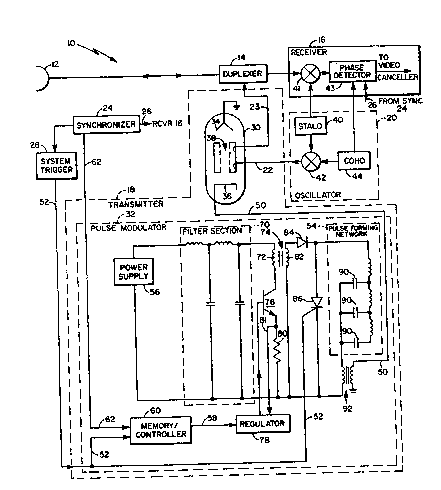
FIG. 1 is a schematic diagram of a radar system according
to the invention;
FIG. 2 is a timing diagram of pulses used by the pulse
modulator of FIG. l; and
FIG. 3 is a schematic diagram of a radar system according
to an alternate embodiment of the invention.
- 13 -
h ~i"", ~3
Description of the Preferred Embodiment
Referring now to FIG. 1, a coherent pulsed Doppler
staggered-PRF, moving target indicator (MTI) radar system 10
has been selected to illustrate how the invention might be
applied. Thus, radar system 10 is adapted to ope~ate with a
selected one of a plurality of pulse repetition intervals.
The pulse repetition interval may be changed on either a scan-
to-scan, batch-to-batch, or pulse-to-pulse basis. The
illustrated radar system 10 includes a radar antenna 12, a
duplexer 14, a radar receiver 16, a radar transmitter 18, an
oscillator 20, a synchronizer 24, and a system trigger 28,
all arranged in a conventional manner as shown whereby,
during transmit modes, synchronizer 24 sends signals to the
system trigger 28 at the selected one of the pulse repetition
intervals, and in response to each one thereof, radio frequency
energy produced by oscillator 20 and coupled to the transmitter
18 via line 22, is amplified and pulse modulated by such
transmitter 18. The amplified and pulsed modulated radio
frequency energy is then coupled to antenna 12 via line 23
and duplexer 14 for transmission. During interleaved received
I modes, portions of the transmitted energy reflected by objects
¦ within the beam of the antenna 12, are received by such
antenna 12 and are passed, via duplexer 14, to the radar
receiver 16 where they are heterodyned and phase detected
with signals produced by oscillator 20 into video signals.
- 14 -
._
~ .~9 ~ , s~
.
The video signals are then resolved into range bins in response
to signals fed to the receiver 20 from synchronizer 24 via
bus 26 for conventional moving target indicator (M~I) processing.
That is, video signals produced by returns from stationary
objects have the same phase shift from pulse-to-pulse while
video signals produced by returns from moving objects have
phase shifts which change from pulse-to-pulse at a rate
related to the velocity of the object. It is noted that
while the antenna 12, duplexer 14, receiver 16, oscillator
20, synchronizer 24 and system trigger 28 are all of conventional
design, the transmitter 18 includes a conventional cathode
pulsed, radio frequency power amplifier tube 30, here a
conventional klystron, controlled by a pulse modulator 32
according to the invention. As shown, the amplifier tube 30
includes a grounded anode 34, a cathode 36 coupled to pulse
modulator 32, and a cavity 38 fed by the oscillater 20, in a
conventional manner. Oscillator 20 includes a stable local
oscillator ~STALO) 40 coupled to, inter alia, mixer 42 along
with coherent local oscillator (COHO) 44~to produce a radio
frequency signal on line 22 to the input to cavity 38 of
klystron 30 in a conventional manner. The outputs of STALO
40 and COHO 44 are also fed to the receiver 16, and in particular
to mixer 41 and phase detector 43, respectively~ The output
in phase detector 43 is ~oupled to a video canceller (not
shown) in a conventional manner, as shown.
- 15 -
.. ._ .. .. . ~
.. ....
,
.
Transmitter 18 includes the pulse modulator 32, here a
high voltage switching circuit adapted to produce output
pulses (i.e., control voltages) on line 50 in response to
trigger pulses fed to such modulator 32 on line 52lvia system
trigger 28. The voltages of the output pulses on line 50
have levels, from trigger pulse to trigger pulse, such that
the relative phase of the transmitted pulses on line 23
will be substantially constant relative to the phase of
the reference signal on line 22, independent of the pulse
repetition interval of such system trigger pulses. The
output pulses (i.e., control voltages) produced on line 50
pulse klystron 30 to a conducting condition to thereby produce
a pulse of radio frequency energy on line 23 and, hence,
enable transmission of such radio frequency pulse via duplexer
14 and antenna 12.
More particularly, the pulse modulator 32 includes a
pulse forming network (PFN) 54 for storing energy from a high
voltage power supply (HVPS) 56 in response to charge con-
trolling signals, here charge initiating pulses~PcI fed to
the modula~or 32 via line 58 and charge~terminating signals
- PCT produced by regulator 78 in response to a voltage level
on line 81. As will be described, pulse forming network
(PFN) 54, in response to these charge controlling signals
PCI~ PCT~ stores energy from the high voltage power supply 56
and produces a train of output pulses on line 50 from such
- 16 -
J ~ J ~3
stored energy in response to a train of trigger pulses PT~
A memory/controller 60, responsive to a signal fed thereto
v;a line 62 by synchronizer 24 and representative of the
pulse repetition interval of the trigger pulses, (and ~ore
particularly the time interval ~l between the last trigger
pulse PTl and the next suceeding trigger pulse PT2 ~FIG. 2))
controls the time interval ~2 between one of the charge
controlling signals, (either PCI or PCT) here, the charge
initiating pulses PCr on line 58 and the trigger pulses P~
line 52. The time interval ~2 is selected to enable
storage, in the pulse forming network 54, of a predetermin~
constant amount of energy at the time of the trigger pulse:)
PT such that transmission of pulses of radio frequen~y ene)~Y
on line 23 will have substantially constant phase, r~lati
lS to the phase of the reference signal produced by mix~r 42
on line 22, over the range of pulse repetition inter~als.
Pulse modulator 32 includes a conventional L-C _ilter
section 70 arranged as shown, and coupled to the ou'?ut of the
i power supply 56 in a conventional manner as shown, ~ pro~ e
I a substantially constant, dc voltage on the upper e-.J of
primary winding 72 of transformer 74. (It should ~e noted
that the level of the voltage at the output of the - lter
section 70 will be because of, inter alia, the int -.al
resistance of power supply 56, a function of the p ,e re~ti~
2S tion interval of the trigger pulses). The base el-: rode
; - 17 -
~ _
circuit of transistor 76 inc'udes a resistor 80. Resistor 80
produces a voltage on line 81 proportional to the current
passing through the emitter of transistor 76. The produced
voltage is fed to a regulator 78, as shown. Regulator 18
initiates a drive pulse response to each charge initiating
pulse PCI on line 58 to turn transistor 76 from a nonconducting
condition to a conducting condition. The current passing through
the emitter electrode of now conducting transistor 76 is sensed,
via the voltage across resistor 80, by regulator 78. When the
voltage across resistor 80 reaches a predetermined voltage lever,
regulator 78 produces the charge terminating signal PCT~ and
terminates the drive pulse at the base electrode of transistor
76 to thereby change the conducting transistor 76 into a non-
conducting mode. Thus, regulator 78 includes a conventional
voltage threshold detector, or comparator circuit (not shown).
The nonconducting-conducting-nonconducting sequence of transistor
76 causes a pulse to be produced in the primary winding 72 of
tranformer 74. Such pulse is inductively coupled to the
secondary winding 82 of transformer 74, and thus, the energy
in such pulse passes through diode 84 for storage in the shunt
connected capacitors 90 of pulse forming network 54.
It should be noted that becauSe the charging rate of the
capacitors 90 is a function of the level of the voltage fed to
such capacitors and since, as noted above, the level of such
voltage is a function of the voltage produced at the output
- 18
__
of filter section 70 (which is a function of the pulse repeti-
tion interval), the rate of charge of such capacitors 90 is
likewise a function of the pulse repetition intervaL. Further,
it should be noted that because there is a small delay between
the time that the threshold voltage is sensed and the time
transistor 76 is actually placed in a nonconducting condition,
additional charging occurs. Since the rate of charging is a
function of the level of the voltage at the time the voltage
level is removed, and such is a function of the pulse repetition
interval, the additional charging stored by the capacitors 90
is also a function of the pulse repetition interval. In
response to the trigger pulse (PT) silicon controlled rectifier
(SCR) 86 conducts causing the energy stored in the capacitors
90 to discharge and thus induce an output voltage on line 50
lS via transformer 92. Memory/controller 60 adjusts the time
interval between the charge controlling pulse, here the charge
initiating pulse PCI produced by regulator 78, relative
to the time of the next trigger pulse PT to be producQd by the
system trigger 28 so that, if there were no subtle effects
from the power amplifier 30 (such as, for a klystron tube,
differential cathode loading and/or klystron cavity differential
heating (or differential cooling) during the interpulse
period) the amount of energy stored in capacitors 90 at the
time of each trigger pulse Tp is substantially constant (and
hence, the voltage level of the output pulses on line 50 will
-- 19 --
2 o ~
be constant) over the range of operating pulse repetition
intervals of such trigger pulses. As will be noted below,
however, that because of these subtle effects associated with
the power amplifier 30, the level of the energy st~red by
such capacitors 90 is such that the transmitted pulses on
line 23 have substantially constant phase, relative to the
phase of the reference signal produced by mixer 42, inde-
pendent of the pulse repetition interval.
Memory/controller 60 includes a conventional read only
memory (not shown). The read only memory (not shown) is
addressed by the signal on line 62. The signal on line 62 is
produced by synchronizer 24 and is representative of the selected
one of the plurality of pulse repetition intervals producible
by the radar system 10. More particularly, such signal on
line 62 is a digital word representative of a time interval ~1'
(FIG. 2) between the current trigger pulse PTl and the next trigger
pulse PT2. Each one of such digital words addresses a corres-
ponding one of a plurality of the locations of the read only
memory. Stored in each one of such locations is a digital
word representative of the time interval ~2 (FIG. 2) between
the next trigger pulse PT2 and the charge control pulse here
the charge initiating pulse PCIll such that either the energy
stored by capacitors 90 at the time of trigger pulse will be
¦ constant (as in the case where pulse repetition interval
variation on the above-mentioned subtle effects can be neglected
- 20 -
in the power amplifier 30) or, the energy will be such that
the phase of the signal produced on line 23 will be
constant relative to the phase of the signal on line 22,
independent of the pulse repetition interval (as in the case
where such subtle effects are to be compensated). This
stored time ~2 interval is determined as a result of a
calibration procedure. More particularly, for each one of
the plurality of time intervals (over the range of permissible
time intervals for the radar system) between successive trigge~
pulses an experimental determination is made of the time
interval ~2 between the charge initiating pulse PCIl and
the next trigger pulse PT2 such that the phase of the radio
frequency pulse produced on line 23 relative to the phase of
the signal on line 22 is substantially constant over the rang-~
lS of pulse repetition intervals. More particularly, for each ol~`
of the permissible pulse intervals between successive trigger
pulses, the phase of the radio frequency energy produced by
oscillator 20 on line 22 is compared with the phase of the ra~
frequency pulse produced on line 23. For each of the plurali~
of possible time intervals Al (FIG. 2) between successive
trigger pulses PTl, PT2 (FIG. 2) the time interval ~2 (FIG. 2'
between the next one of the trigger pulses, PT2, and the char~`
initiating pulse PCIl is varied so that the phase between
the signal on line 23 and the signal produced on line 22 by
oscillator 20 is constant over the plurality of possible time
- 21 -
__
_~ ~
: ~-
~P~ j 3
_~
~`
F intervals between successive trigger pulses. The determined
time intervals ~2 (FIG. 2) for each one of the plurality of
possible time intervals ~1 (FIG. 2) are stored in the read
only memory (not shown) of the memory/controller 60J
Referring now to FIG. 3 a radar system 10' is shown to
again include a radar antenna 12, a duplexer 14, a radar
receiver 16, a radar transmitter 18', a synchronizer 24, and
a system trigger 28 all arranged as shown in a conventional
manner. Here, however, transmitter 18', while including the
pulse modulator 32 shown and described in detail in connection
with FIG. 1, includes a high power radio frequency energy
oscillator, here a magnetron 30'. The magnetron 30' is pulsed
on and off in response to the pulse (i.e., control voltage)
produced by the pulse modulator 32 on line 50. The radio fre-
quency pulse produced by the magnetron 30' in response to pulses
produced on line 50 is fed, via line 23', to the duplexer 14.
A portion of such produced pulse is fed, via directional coupler
51, to mixer 42'. Also fed to mixer 42' is a signal produced
by STALO 40. The output of mixer 42' is fed to OOHO 44'. The
output of STALO 40 is also fed to mixer 41 of radar receiver 16.
The output of mixer 41, along with the output of COHO 44', are
fed to phase detector 43, the output of such phase detector 43
being a video signal which is fed to a video canceller (not shown)
in a conventional manner. Here the radar system 10' is calibrated
so that over the range of operating pulse repetition intervals,
~ h~ . 3
J~'
/ a value ~2 (FIG. 2) is stored in the memory/contr~ller 60
of pulse modulator 32 such that magnetron 30' produces on line
23' pulses of the same freguency for each one of the pulse
7 repetition intervals in the range thereof. In this manner,
r 5 for each pulse repetition interval selected, the phase of the
video signal produced by the phase detector 43 in response to
returns from stationary objects will be constant relative to
the phase of the signal fed to the phase detector 43 by COHO 44.
Having described the preferred embodiment of the invention
it will now be apparent to one of skill in the art that other
embodiments incorporating its concepts may be used. For example,
instead of varying the time of the charge initiating pulse PCI
relative to the time of the next succeeding trigger pulse, one
could vary the time the charging process is stopped relative
to the next trigger pulse (i.e. varying the time interval
between the charge terminating signal, PCTl~ and PT2 in FIG.
2) instead oE sensing the voltage across resistor 80. That
is, the charge control pulse can be used to change the termin-
ating pulse by changing the voltage threshold of the voltage
comparator (not shown) in regulator 78 (FIG. 1) as a function
of pulse repetition interval. Further, when the dielectric
absorption in the capacitors 90 are insufficient to compensate
for the phase shifts, a bleed-down resistor may be put in
parallel with these capacitors 90 so that changing the charge
initiating timing will provide more compensation for the
- 23 -
__
I
/ pulse-to-pulse ph~se shifts o~ t~s transritter outp~t. It is
felt therefore, that this invention should not be restricted
to the disclosed embodiment but rather should be limited only
by the spirit and scope of the appended claims. I
_ 24 ~
.
__
~_. ~ ~
~ _~