Note: Descriptions are shown in the official language in which they were submitted.
202~562
~~r 1 ' _
OPTICAL HEAD FOR OPTICAL INFORMATION RECORDING MEDIUM
- The present invention relates to an optical head
used for recording information onto an optical
information recording medium, and playing back
information therefrom.
BACKGROUND OF THE INVENTION
(Description of the Prior Art)
In the conventional method of recording information
onto an optical information recording medium (hereinafter
abbreviated to "recording medium") and playing back
information from that recording mediumr an optical head
of an optical-system construction is used, such as that
shown in Fig. 14. The operation of the optical system of
the optical head of Fig. 14 is described below. First, a
divergent beam of light 2 emitted from a semiconductor
laser 1 is converted by a collimator lens 3 into a
parallel beam of light 4, and the parallel beam of light
4 is incident on a diffraction grating 5 and is converted
thereby into three transmission diffraction beams of
light at dimensions 0 and il.
These three transmission diffraction beams of light,
in other words, three light beams 6, are incident on a
beam splitter 7 and are both passed and reflected by a
semi-transparent diaphragm 8 of the beam splitter 7.
Three beams of light 9 that are passed by the beam
splitter 7 are focused by a focusing lens 10 into three
very small spots of light 11 (hereinafter abbreviated to
"light spots") arranged on a straight line, and are shone
onto a recording medium 12. In this case, a high-output
beam of light from the semiconductor laser 1 modulated by
an information signal is used to record information, and
a continuous low-output beam of light is used to play
back the information. The central light spot of the
three light spots 11 arranged in a straight line is a
main light spot that is a 0-dimensional diffraction light
-"
-
~ ` 2 2028~
spot used for recording and playing back information and
for focusing, and the two auxiliary spots of light
positioned on either side thereof are +l-dimensional
diffraction spots of light used for tracking.
The three beams of light shone onto the recording
medium 12 as the three light spots 11 are partially
reflected thereby, and the resultant three reflected
beams of light are passed back through the focusing lens
10 which converts them back into approximately parallel
beams of light. These beams of light are reflected by
the semi-transparent diaphragm 8 of the beam splitter 7
to the right in the figure, are condensed by a
photoreceiver lens 13, and reach a photoreceiver diode 15
through a cylindrical lens 14. An information signal, a
focusing control signal that indicates the focusing
status of the light spots 11, and a tracking control
signal that indicates the positional status between a
track provided on the recording medium 12 and the light
spots 11 are obtained from the light-receiving diode 15.
Note that the photoreceiver lens 13 is an optical element
that acts to condense the three reflected parallel beams
of light, and the cylindrical lens 14 is an optical
element in which astigmatism occurs in order to provide a
focusing control signal. Thus, the optical head shown in
Fig. 14 uses an astigmatism method to derive a focusing
control signal and a three-beam method to derive a
tracking control signal.
(Problem to be Solved by the Present Invention)
The optical head of the above optical-system
construction is widely used at present, but it has the
defect that good focusing cannot be obtained because the
astigmatism method used in focusing leads to a large
amount of cross-talk. In other words, the tracking
control signal leaks badly into the focusing control
signal.
This leakage is due to the fact that, if the
focusing lens 10 is driven in the direction perpendicular
~ 2028562
20375-674
ln the tracks provlded on the recordlng medlum 12, to ensure
tracklng, the light spots of the beams of llght recelved by the
photoreceiver diode 15 will also move. In other words, when
both the astlgmatlsm method and the three-beam method are used
together, the photorecelver dlode 15 ls formed of a divlded
element structure consistlng of six elements 15A to 15F, and
three llght spots conslstlng of a light spot 16 from the main
beam of llght and llght spots 17 and 18 from the auxlllary beams
of llght are shone onto the photoreceiver diode 15, as shown in
Fig. 15. If the focuslng len~ 10 ls drlven to ensure tracking,
these three light spots wlll move ln the direction indlcated by
the X arrows, to become llght spots 16', 17', and 18', for
example.
If there is a non-focused condltlon, partlcularly due
to the fact that the gap between the focuslng lens 10 and the
recordlng medlum 12 ls sllghtly changed and the llght spot 16 on
the photorecelver diode 15, used to derlve the focuslng control
slgnal, has become elllptlcal-shaped, as shown ln Flg. 16, the
result of the equatlons
[(element 15A output + element 15B output) -
telement 15C output + element 15D output) - focuslng
control slgnal output]
used to derlve the focuslng control slgnal output wlll dlffer
between the cases ln whlch the llght spot ls the elllptical
llght spot 16 and the elllptlcal llght spot 16', and thus cross-
talk wlll be generated.
2028562
20375-674
SUMMARY OF THE INVENTION
The purpose of the present inventlon ls to provlde an
optical head ln which cross-talk does not occur, ln other words,
in whlch a tracking control slgnal does not leak lnto a focuslng
control signal, even when the focuslng lens 10 ls drlven to
enable tracklng.
(Means of Accomplishlng the Present Inventlon)
The above purpose ls achleved by the optical head of
the present invention which comprises an illumlnatlon system
whlch shlnes three beams of light comprising 0-dimensional
diffraction llght, +l-dlmenslonal diffraction llght, and -1-
dlmenslonal diffractlon llght onto an optlcal lnformatlon
recordlng medlum, and a photorecelver system whlch recelves
three beams of reflected light from sald recordlng medlum; sald
photoreceiver system being provlded wlth an edge mlrror whereby,
of said three beams of reflected light from sald recording
medium, approximately one half of said 0-dimensional dlffraction
llght and all of said +l-dimensional diffraction light is
received by a flrst photoreceiver dlode, wlthout being affected
by sald edge mlrror, and the remainlng approxlmately one half of
said 0-dimenslonal diffractlon light and all of sald -1-
dimenslonal diffractlon llght ls reflected by sald edge mlrror
and is recelved by a second photorecelver dlode; wherein a
focusing control slgnal, a tracklng control signal, and an
lnformatlon slgnal are obtalned from an output from sald flrst
photorecelver dlode or sald second photorecelver dlode, or from
comblned outputs from sald flrst photorecelver dlode and sald
2028562
~'
20375-674
second photorecelver diode.
In a preferred embodiment the focusing control signal
and the lnformation signal are obtained from the 0-dlmensional
diffraction light, and the tracklng control signal is obtained
from the +l-dimensional diffraction light and the -l-dimensional
diffraction light.
The photoreceiver diodes that extract the focuslng
control signal may each have an element construction that is
divided into two parts, with the division line therebetween
posltloned parallel to the edge of the edge mlrror. When the
focusing lens is driven to enable tracking, the light spots on
the photoreceiver diodes move parallel to the divlsion line, so
there ls no change in the output from each element and thus
cross-talk does not occur.
When an edge mlrror dlvides a beam of llght lnto two
parts, the optlcal energy ls also halved. Therefore, the
present lnvention combines photoreceiver output from direct
light that has not been affected by the edge
4a
2028562 = ~
` 5
mirror with photoreceiver output from light that has been
reflected from the edge mirror, to prevent any drop in
- efficiency.
The information signal is also obtained from the
two-element photoreceiver diodes that derive the focusing
control signal.
The photoreceiver diodes that extract the tracking
control signal are positioned in close contact with the
photoreceiver diodes used to extract the focusing control
signal, and the tracking control signal is obtained from
a combination of differences between photoreceiver
outputs from a direct light side which is not affected by
the edge mirror and a reflected light side which is
reflected from the edge mirror.
BRIEF DESCRIPTION OF THE DRAWINGS
In the accompanying drawings, Fig. 1 shows the
optical-system construction of the optical head of the
present invention; Figs. 2, 3, Ç, and 7 show examples of
photoreceiver diodes composed of three elements, and the
light spots received thereby; Figs. 4 and 5 are diagrams
that illustrate the paths of beams of light in the
optical system used to derive a focusing control signal
and a tracking control signal; Figs. 8 and 9 show
examples of photoreceiver diodes composed of four
elements, and the light spots received thereby; Figs. 10
and 11 show examples of circuit configurations for
creating a focusing control signal, a tracking control
signal, and an information signal from the outputs of the
photoreceiver diodes; Fig. 12 is a diagram used to
illustrate focusing control and tracking control; Fig. 13
is perspective drawings of edge mirrors; Fig. 14 shows an
example of the optical-system construction of a
conventional optical head; Fig. 15 shows the structure of
a conventional photoreceiver diode and the light spots
received thereby; and Fig. 16 illustrates a case in which
the light spots of Fig. 15 have become ellipses, wherein
movement of the light spots causes cross-talk.
202856~
DESCRIPTION OF T~E PREFERRED EMBODIMENT
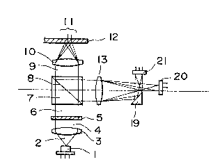
Figure 1 shows the optical-system construction of
- the optical head of the present invention. The optical
head of Fig. 1 is constructed of a semiconductor laser 1,
a collimator lens 3, a diffraction grating 5, a beam
splitter 7, a focusing lens 10, a photoreceiver lens 13,
an edge mirror 19, and photoreceiver diodes 20 and 21.
The operation of the optical head of Fig. 1 is
described below. A divergent beam of light 2 emitted
from the semiconductor laser 1 is converted by the
collimator lens 3 into a parallel beam of light 4, and
the parallel beam of light 4 is incident on the
diffraction grating 5 and is converted thereby into three
transmission diffraction beams of light at dimensions 0
and +1.
These three transmission diffraction beams of light,
in other words, three light beams 6, are incident on the
beam splitter 7 and are both passed and reflected by a
semi-transparent diaphragm 8 of the beam splitter 7.
(The ratio of strengths of the transmitted light and
reflected light need not be 1, and the three reflected
beams of light can be either absorbed or scattered.)
Three beams of light 9 that are passed by the beam
splitter 7 are focused by the focusing lens 10 into three
light spots 11 arranged on a straight line, and are shone
onto a recording medium 12. In this case, a high-output
beam of light from the semiconductor laser 1 and
modulated by an information signal is used to record
information, and a continuous low-output beam of light is
used to play back the information. The central light
spot of the three light spots 11 arranged in a straight
line is a main light spot that is a 0-dimensional
diffraction light spot used for recording and playing
back information and for focusing, and the two auxiliary
spots of light positioned on either side thereof are the
+l-dimensional diffraction spots of light used for
tracking.
7 202856~ -
The three beams of light shone onto the recording
medium 12 as the three light spots 11 are partially
rreflected therebyr and the resultant three reflected
beams of light are passed back through the focusing lens
5 10 which converts them back into approximately parallel
beams of light. (Depending on the focusing state, these
could become slightly convergent beams of light or
slightly divergent beams of light.) These beams of light
are reflected by the semi-transparent diaphragm 8 of the
10 beam splitter 7 to the right in the figure, are condensed
by a photoreceiver lens 13, and are divided in such a
manner that, for example, half of the 0-dimensional
diffraction light and all of the +l-dimensional
diffraction light pass straight through the edge mirror
15 19, without being affected thereby, and reach the first
photoreceiver diode 20 which is positioned in close
proximity to the focal point of the photoreceiver lens
13, and the remaining half of the 0-dimensional
diffraction light and all of the -l-dimensional
20 diffraction light are reflected by the edge mirror 19 and
reach the second photoreceiver diode 21 which is also
positioned in close proximity to the focal point of the
photoreceiver lens 13.
Figures 2 and 3 show examples of the structure of
25 the photoreceiver diodes 20 and 21. The photoreceiver
diode 20 is constructed of elements 20A, 20B, and 20C, as
shown in Fig. 2, with the 0-dimensional diffraction light
shining onto the elements 20A~ and 20B, and the +1-
dimensional diffraction light shining onto the element
30 20C. Similarly, the photoreceiver diode 21 is
constructed of elements 21A, 21B, and 21C, as shown in
Fig. 3, with the 0-dimensional diffraction light shining
onto the elements 21A and 21B, and the -l-dimensional
diffraction light shining onto the element 21C.
The paths of beams of light through the optical
system used to derive the focusing control signal and the
tracking control signal are shown in Fig. 4.
-
-
` 8 202~5G2
If the recording medium 12 shown in Fig. 1 is
positioned at the focused position of the focusing lens
10, the three beams of light shone onto the recording
medium 12 and partially reflected therefrom pass back
through the focusing lens 10 and become parallel beams of
light. They are then reflected by the semitransparent
diaphragm 8 of the beam splitter 7 and are incident on
the photoreceiver lens 13 in such a manner that the 0-
dimensional diffraction light becomes a parallel beam of
light 22, the +l-dimensional diffraction light becomes a
parallel beam of light 23, and the -l-dimensional
diffraction light becomes a parallel beam of light 24, as
shown in Fig. 4(a).
If the recording medium 12 moves closer to the
focusing lens 10l the three beams of light are incident
on the photoreceiver lens 13 in such a manner that the
0-dimensional diffraction light becomes a divergent beam
of light 25, the +l-dimensional diffraction light becomes
a divergent beam of light 26, and the -l-dimensional
diffraction light becomes a divergent beam of light 27,
as shown in Fig. 4(b).
If the recording medium 12 moves further away from
the focusing lens 10, the three beams of light are
incident on the photoreceiver lens 13 in such a manner
that the 0-dimensional diffraction light becomes a
convergent beam of light 28, the +l-dimensional
diffraction light becomes a convergent beam of light 29,
and the -l-dimensional diffraction light becomes a
convergent beam of light 30, as shown in Fig. 4(c).
In the state shown in Fig. 4(a), the parallel beam
of light 22 incident on the photoreceiver lens 13 is
condensed by the photoreceiver lens 13, and the upper
half of the light condensed by the photoreceiver lens 13
proceeds past the edge mirror 19, without being affected
thereby, to reach a boundary portion between the elements
20A and 20B of the photoreceiver diode 20, forming a very
small light spot 32 on a boundary line 31 therebetween,
` 9
2028562
as shown in Fig. 2. Therefore, no photoreceiver output
is obtained from either the element 20A or the element
- 20B (in practice, diffraction and other phenomena will
result in a certain amount of light shining on the
elements 20A and 20B, but the photoreceiver output
obtained therefrom will be approximately equal). The
lower half of the light condensed by the photoreceiver
lens 13 is reflected by the edge mirror 19 and reaches a
boundary portion between the elements 21A and 21B of the
photoreceiver diode 21, forming a very small light spot
34 on a boundary line 33 therebetween, as shown in Fig.
3. Therefore, no photoreceiver output is obtained from
either the element 21A or the element 21B (in the same
way as described above, a certain amount of light will
shine thereon, but the photoreceiver outputs obtained
therefrom will be approximately equal).
The focusing control signal is derived from the
photoreceiver diodes 20 and 21 according to one of the
following equations:
(Element 20A output + element 21A output) - (element
20B output + element 21B output) = focusing control
signal output [Equation 1]
(Element 20B output + element 21B output) - (element
20A output + element 21A output) = focusing control
signal output [Equation 2]
so that, in the case shown in Fig. 4(a), the focusing
control signal output is zero.
Similarly, the parallel beam of light 23 and the
parallel beam of light 24 incident on the photoreceiver
lens 13 are condensed by the photoreceiver lens 13. The
parallel beam of light 23 reaches the element 20C of the
photoreceiver diode 20 and forms a very small light spot
35 on the element 20C, as shown in Fig. 2, and part of
the parallel beam of light 24 that is reflected by the
edge mirror 19 reaches the element 21C of the
photoreceiver diode 21 and forms a very small light spot
36 on the element 21C, as shown in Fig. 3. The resultant
~ lo 2~28562
photoreceiver outputs are used to derive the tracking
control signal according to one of the following
e~uations:
Element 20C output - element 21C output = tracking
control signal output [Equation 3]
Element 21C output - element 20C output = tracking
control signal output [Equation 4]
In the state shown in Fig. 4(b), the divergent beam
of light 25 incident on the photoreceiver lens 13 is
condensed by the photoreceiver lens 13, and the upper
half of the light condensed by the photoreceiver lens 13
proceeds past the edge mirror 19, without being affected
thereby, to reach the element 20A of the photoreceiver
diode 20, forming a semi-circular light spot 37 on the
element 20A, as shown in Fig. 2. The lower half of the
light condensed by the photoreceiver lens 13 is reflected
by the edge mirror 19 then reaches the element 21A of the
photoreceiver diode 21, forming a semi-circular light
spot 38 on the element 21A, as shown in Fig. 3. The
focusing control signal is derived from either Equation 1
or Equation 2. In the same way, the divergent beams of
light 26 and 27 incident on the photoreceiver lens 13 are
condensed by the photoreceiver lens 13. The divergent
beam of light 26 reaches the element 20C of the
photoreceiver diode 20 and forms a light spot 39 on the
element 20C, as shown in Fig. 2, and part of the
divergent beam of light 27 that is reflected by the edge
mirror 19 reaches the element 21C of the photoreceiver
diode 21 and forms a light spot 40 on the element 21C, as
shown in Fig. 3. The tracking control signal is derived
from either Equation 3 or Equation 4.
In the state shown in Fig. 4(c), the convergent beam
of light 28 incident on the photoreceiver lens 13 is
condensed by the photoreceiver lens 13, and the upper
half of the light condensed by the photoreceiver lens 13
proceeds past the edge mirror 19, without being affected
thereby, to reach the element 20B of the photoreceiver
~ ~ 11 2028562
diode 20, forming a semi-circular light spot 41 on the
element 20B, as shown in Fig. 2. The lower half of the
- light condensed by the photoreceiver lens 13 is reflected
by the edge mirror 19, contracts to the focal point then
expands again, and finally reaches the element 21B of the
photoreceiver diode 21, forming a semi-circular light
spot 42 on the element 21B, as shown in Fig. 3. The
focusing control signal is derived from either Equation 1
or Equation 2. In the same way, the convergent beams of
light 29 and 30 incident on the photoreceiver lens 13 are
condensed by the photoreceiver lens 13. The convergent
beam of light 29 focuses to the focal point then expands
again, and finally reaches the element 20C of the
photoreceiver diode 20 and forms a light spot 43 on the
element 20C, as shown in Fig. 2, and the convergent beam
of light 30 is reflected by the edge mirror 19, focuses
to the focal point then expands again, and finally
reaches the element 21B of the photoreceiver diode 21 and
forms a light spot 44 on the element 21C, as shown in
Fig. 3. The tracking control signal is derived from
either Equation 3 or Eguation 4.
As described above, if the recording medium 12 is
positioned at the focused position of the focusing lens
10, both of the photoreceiver diodes 20 and 21 are
positioned in close proximity to the focal point of the
photoreceiver lens 13, but in fact the photoreceiver
diodes 20 and 21 do not necessarily need to be positioned
close to the focal point of the photoreceiver lens 13.
Similarly, the edge mirror 19 shown in Fig. 4 is
positioned with a linear edge portion 45 thereof
perpendicular to the plane of the figure and in contact
with an optical axis 46, but the edge mirror 19 could be
moved a suitable distance in the vertical direction shown
in Fig. 4 (Y direction) or along the optical axis (Z
direction). In addition, the photoreceiver diodes 20 and
21 could be moved suitable distances in either the Y
direction or the Z direction.
~ 12 2028562
If the photoreceiver diodes 20 and 21 are not
positioned close to the focal point of the photoreceiver
lens 13, the paths of beams of light in the resultant
optical system will be as shown in Fig. 5. In this case,
the edge mirror 19 is moved a suitable distance in the Z
direction and the photoreceiver diodes 20 and 21 are
moved suitable distances in both the Y and Z directions,
in comparison with their positions in Fig. 4.
Figures 6 and 7 show the light spots formed on the
photoreceiver diodes 20 and 21 positioned as shown in
Fig. 5.
In the state shown in Fig. 5(a), the parallel beam
of light 22 incident on the photoreceiver lens 13 is
condensed by the photoreceiver lens 13, and the upper
15 half of the light condensed by the photoreceiver lens 13
proceeds past the edge mirror 19, without being affected
thereby, to reach the photoreceiver diode 20, forming a
semi-circular light spot 47 extending over the elements
20A and 20B with equal amounts of light shining on the
20 elements 20A and 20B, as shown in Fig. 6. The lower half
of the light condensed by the photoreceiver lens 13 is
reflected by the edge mirror 19 and reaches the
photoreceiver diode 21, forming a semi-circular light
spot 48 extending over the boundary line 33 between the
25 elements 21A and 21B with equal amounts of light shining
on the elements 21A and 21B, as shown in Fig. 7. The
focusing control signal is derived from either Equation 1
or Equation 2. However, in this case, the focusing
control signal output is zero. In the same way, the
30 parallel beams of light 23 and 24 incident on the
photoreceiver lens 13 are condensed by the photoreceiver
lens 13. The parallel beam of light 23 reaches the
photoreceiver diode 20 and forms a light spot 49 on the
element 20C, as shown in Fig. 6, and the parallel beam of
35 light 24 is reflected by the edge mirror 19 then reaches
the element 21C of the photoreceiver diode 21, forming a
light spot 50 on the element 21C, as shown in Fig. 7.
~ 13
202856~
The tracking control signal is derived from either
Equation 3 or Equation 4.
- In the state shown in Fig. 5(b), the divergent beam
of light 25 incident on the photoreceiver lens 13 is
condensed by the photoreceiver lens 13, and the upper
half of the light condensed by the photoreceiver lens 13
proceeds past the edge mirror 19, without being affected
thereby, to reach the photoreceiver diode 20, forming a
semi-circular light spot 51 extending over the element
20a and the element 20B, with the quantity of light
shining on the element 20A being greater than that
shining on the element 20B, as shown in Fig. 6. The
lower half of the light condensed by the photoreceiver
lens 13 is reflected by the edge mirror 19 then reaches
the element 21A of the photoreceiver diode 21, forming a
semi-circular light spot 52 on the element 21A and the
element 21B, with the quantity of light shining on the
element 21A being greater than that shining on the
element 21B, as shown in Fig. 7. The focusing control
signal is derived from either Equation 1 or Equation 2.
In the same way, the divergent beams of light 26 a-nd 27
incident on the photoreceiver lens 13 are condensed by
the photoreceiver lens 13. The divergent beam of light
26 reaches the element 20C of the photoreceiver diode 20
and forms a light spot 53 on the element 20C, as shown in
Fig. 6, and the divergent beam of light 27 is reflected
by the edge mirror 19 then reaches the element 21C of the
photoreceiver diode 21, forming a light spot 54 on the
element 21C, as shown in Fig. 7. The tracking control
signal is derived from either Equation 3 or Equation 4.
In the state shown in Fig. 5(c), the convergent beam
of light 28 incident on the photoreceiver lens 13 is
condensed by the photoreceiver lens 13, and the upper
half of the light condensed by the photoreceiver lens 13
proceeds past the edge mirror 19, without being affected
thereby, to reach the photoreceiver diode 20, forming a
small semi-circular light spot 55 on only the element
~ 14 2028562
20B, as shown in Fig. 6. The lower half of the light
condensed by the photoreceiver lens 13 is reflected by
the edge mirror 19 then reaches the photoreceiver diode
21, forming a small semi-circular light spot 56 on only
the element 21B, as shown in Fig. 7. The focusing
control signal is derived from either Equation 1 or
Equation 2. In the same way, the convergent beams of
light 29 and 30 incident on the photoreceiver lens 13 are
condensed by the photoreceiver lens 13. The convergent
beam of light 29 reaches the element 20C of the
photoreceiver diode 20 and forms a small light spot 57 on
the element 20C, as shown in Fig. 6, and the convergent
beam of light 30 is reflected by the edge mirror 19 then
reaches the element 21C of the photoreceiver diode 21 and
forms a small light spot 58 on the element 21C, as shown
in Fig. 7. The tracking control signal is derived from
either Equation 3 or Equation 4.
The photoreceiver diode 20 is constructed of the
elements 20A, 20B, and 20C, as shown in Figs. 2 and 6,
with the elements 20a and 20B receiving the 0-dimensional
diffraction light and the element 20C receiving the +1-
dimensional diffraction light. The -l-dimensional
diffraction light is reflected by the edge mirror 19 then
is received by the element 21C of the photoreceiver diode
21, as described above.
However, in practice, not all of the -l-dimensional
diffraction light is reflected by the edge mirror 19; a
component thereof leaks toward the photoreceiver diode 20
side. For this reason, the photoreceiver diode 20 is
provided with another element 20D, as shown in Fig. 8,
and the leaking component of the -l-dimensional
diffraction light forms light spots 36', 40', and 44' on
the element 20D. This arrangement is designed to enable
the resultant output to be combined with the
photoreceiver output of the element 21C of the
photoreceiver diode 21 to increase the photoreceiver
efficiency.
2028562
Similarly, the photoreceiver diode 21 is constructed
of the elements 21A, 21B, and 21C, as shown in Figs. 3
- and 7, with the elements 21A and 21B receiving the
0-dimensional diffraction light after it has been
reflected by the edge mirror 19, and the element 21C
receiving the -l-dimensional diffraction light. The +1-
dimensional diffraction light is received by the element
20C of the photoreceiver diode 20, without being affected
by the edge mirror 19, as described above.
10However, in practice, the +l-dimensional diffraction
light is- also affected by the edge mirror 19, and a
component thereof leaks toward the photoreceiver diode 21
side. For this reason, the photoreceiver diode 21 is
provided with another element 21D, as shown in Fig. 9,
and the leaking component of the +l-dimensional
diffraction light forms light spots 35', 39', and 43' on
the element 21D. This arrangement is designed to enable
the resultant output to be combined with the
photoreceiver output of the element 20C of the
photoreceiver diode 20 to increase the photoreceiver
efficiency.
Note that the above reception of light from the
leakage components by providing the elements 20D and 21D
of the photoreceiver diodes 20 and 21 can also be applied
to the photoreceiver diodes shown in Figs. 6 and 7.
The focusing control signal, the tracking control
signal, and also the information signal are derived from
the photoreceiver diodes 20 and 21.
The circuit constructions shown in Figs. 10 and 11
are used to derive the focusing control signal, the
tracking control signal, and the information signal.
In Figs. 10 and 11, the photoreceiver outputs of the
element 20A of the photoreceiver diode 20 and the element
21A of the photoreceiver diode 21 are first added by an
adder 59, and the photoreceiver outputs of the element
20B of the photoreceiver diode 20 and the element 21B of
the photoreceiver diode 21 are added by an adder 60.
` 16 2028562
Outputs from the adders 59 and 60 are input to a
subtractor 61, and the subtractor 61 derives the
difference between the output from the adder 59 and the
output from the adder 60 to obtain a focusing control
5 signal output 62. Note that the focusing control signal
output 62 could also be calculated according to the
following equation, using two subtractors and one adder:
(Element 20A output - element 20B output) + (element
21A output - element 21B output) = (element 20A
output - element 21B output) ~ (element 21A output -
element 20B output) = focusing control signal
output [Equation 5]
Next, to obtain the tracking control signal output
from the circuit of Fig. 10, the photoreceiver outputs of
the element 20C of the photoreceiver diode 20 and the
element 21C of the photoreceiver diode 21 are input to a
subtractor 63, and the difference between these two
photoreceiver outputs is derived by a subtractor 63 to
obtain a tracking control signal output 64. Either
20 Equation 3 or Equation 4 expresses how this output is
derived.
In the circuit shown in Fig. 11, the photoreceiver
outputs of the element 20C of the photoreceiver diode 20
and the element 21D of the photoreceiver diode 21 are
25 added by an adder 65, the photoreceiver outputs of the
elements 21C and 20D are added by an adder 66, outputs
from the adders 65 and 66 are input to a subtractor 67,
and the subtractor 67 derives the difference between
these two inputs as a tracking control signal output 68.
30 This is expressed by the following equation:
(Element 20C output + element 21D output) - (element
21C output + element 20D output) = tracking control
signal output [Equation 6]
Note that the tracking control signal output 68
35 could also be calculated according to the following
equation, using two subtractors and one adder:
17 -~
2~2856~ ~
(Element 20C output - element 21C output) ~ (element
21D output - element 20D output) = (element 20C
output - element 20D output) + (element 21D output -
element 21C output) = tracking control signal
output [Equation 7]
The information signal output is obtained from the
circuits of Figs. 10 and 11 by inputting the outputs from
the adders 59 and 60 to an adder 69, and extracting the
output from the adder 69 as an information signal 70.
The output 62 from the subtractor 61 of Figs. 10 and
11, in other words, the focusing control signal output
62, is suitably amplified by a servo amplifier 71 shown
in Fig. 12 and is applied to a focusing coil 73 to drive
the focusing lens 10 of the optical head along the
optical axis in the directions shown by arrows 72. This
forms a focusing control loop, to control the system to
ensure that sharp light spots are always shone onto the
recording medium 12.
The output 64 from the subtractor 63 or the output
68 from the subtractor 67 of Figs. 10 and 11, in other
words, the tracking control signal output 64 or 68, is
suitably amplified by a servo amplifier 74 shown in Fig.
12 and is applied to a tracking coil 76 to drive the
focusing lens 10 of the optical head perpendicular to the
optical axis in the directions shown by arrows 75. This
forms a tracking control loop, to control the system to
ensure that the light spots accurately trace the tracks
provided on the recording medium 12.
The edge mirror 19 could be a right triangular prism
with a linear edge portion 77, as shown in Fig. 13(a), in
which an inclined surface 78 thereof is employed as a
reflection diaphragm. It could also be as shown in Fig.
13(b) in which the prism is beveled to form a linear edge
portion 79, to prevent the generation of chips and other
defects in the edge portion.
The beam splitter 7 has been described above as a
beam splitter that uses a semi-transparent diaphragm 8,
~ . 18 2028562
but any suitable light isolator such as a polarized beam
splitter using a polarized membrane and a l/4-wavelength
plate could be used instead. Such light isolators would
help to reduce optical losses and also reduce the return
of light back toward the semiconductor laser 1. In
addition, the photoreceiver diodes 20 and 21 have been
described above as "diodes", but it should go without
saying that any other type of photoreceiver elements,
such as solar cells, could be used instead.
The above description shows how the photoreceiver
outputs of the photoreceiver diodes 20 and 21 are
combined from consideration of the efficiency of
obtaining the focusing control signal. However, if
importance is placed on an easy-to-adjust system, rather
than a more efficient system, either the photoreceiver
output from the photoreceiver diode 20 alone or the
photoreceiver output from the photoreceiver diode 21
alone could be used. In other words, either of the
following equations could be used:
ielement 20A output ~element 20B output = focusing
control signal output
ielement 21A output ~element 21B output = focusing
control signal output
(Effect of the Present Invention)
As described above, the present invention enables
the provision of an optical head in which a focusing
control signal is derived by using an edge mirror and
photoreceiver diodes that are divided into two parts, so
no cross-talk is generated even when the focusing lens is
driven to ensure tracking. In addition, since an edge
mirror is used, both a beam of light that travels
directly and a beam of light reflected by the edge mirror
can be utilized efficiently without any losses, making
this optical head suitable for a three-beam method with
an excellent level of stability.
-