Note: Descriptions are shown in the official language in which they were submitted.
1- 2o29872
SPECIFICATION
CLOCK GENERATING APPARATUS
TECHNICAL FIELD
The present invention relates generally to clock
generating apparatuses. More specifically, the present
invention relates to a clock signal generating apparatus
for application in a writing clock generating circuit of a
time base corrector or the like for generating a clock
signal by synchronizing an externally applied horizontal
synchronizing signal with a reference synchronizing
signal.
BACKGROUND ART
In recording a video signal on an optical disc or in
a video tape recorder in the form of an analogue signal
and reproducing the same, a time base corrector is used
for removing time base fluctuation of the reproduced video
signal.
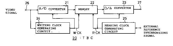
Fig. 1 is a schematic block diagram showing one
example of a conventional time base corrector. Referring
to Fig. 1, a terminal 26 receives a reproduced video
signal (still picture signal) having a time base
fluctuated. This reproduced video signal is applied to an
A/D convertor 21 and a writing clock generating circuit
24. Writing clock generating circuit 24 separates a
horizontal synchronizing signal from the reproduced video
-- 1 -- ~,,
~.~
2029872
signal and also generates a writing clock signal W-CK
corresponding to a time base fluctuation of the reproduced
video signal. In response to the writing clock signal
W-CK, A/D convertor 21 samples the reproduced video signal
and digitalizes the same to be applied to a memory 22.
Memory 22 writes the digitalized video signal in response
to the writing clock signal W-CK having the same time base
fluctuation.
Meanwhile, an external reference synchronizing signal
is applied to a reading clock generating circuit 25, which
circuit generates a reading clock signal R- CK
synchronizing with the external reference synchronizing
signal having a fixed time base, which clock signal is
applied to memory 22 and a D/A convertor 23. In response
to the reading clock signal R-CK, memory 22 reads the
stored digital video signal and applies the same to D/A
convertor 23. In response to this reading clock signal
R-CK, D/A convertor 23 converts the digital video signal
to an analogue signal. Therefore, the video signal output
from D/A convertor 23 to an output terminal 27 has a fixed
time base.
Time base correcting capability of such a time base
corrector as shown in Fig. 1 depends on whether the
writing clock signal W-CK can be generated or not which
precisely corresponds to a time base fluctuation of the
202~ 872
reproduced video signal. A conventionally proposed common
BCO ~burst controlled oscillator) using such elements as a
crystal oscillator, a coil and a capacitor is not
satisfactory and therefore required is a circuit having a
wide frequency response range and a high response speed.
Such a BCO is essentially liable to become unstable
affected by noise, waveform distortion, drop out or skew.
Thus, various improvements have been made in a burst
gate circuit or a synchronization separating circuit
included in a time base corrector in order to prevent
attenuation of a time base fluctuation component of an
input video signal while reducing an effect of noise or
the like. For example, used as a horizontal synchronizing
signal separating circuit are a delay circuit, a
synchronization gate circuit employing a gate signal and
comprising a flywheel oscillator, and such a circuit as
detecting drop out to mute the drop out noise in a video
signal and inhibiting synchronization separating or
clamping. A wide-band circuit is used as a color burst
gate circuit for amplifying and separating a synchronizing
signal and a color burst signal.
Fig. 2 shows one example of a case where a precise
reading clock signal W-CK is generated by using thus
separated synchronizing signal and color burst signal.
In a writing clock generating circuit 24 shown in
2029872
Fig. 2, a horizontal synchronizing signal is applied to a
phase comparator 31 through a terminal 40. Phase
comparator 31 compares the phase of the horizontal
synchronizing signal with that of a signal obtained by
frequency-dividing an output of a variable voltage
controlled oscillator (VCO) 33 by a frequency-dividing
circuit 34 to apply an error voltage to VCO 33 through a
loop filter 32. Phase comparator 31, loop filter 32, VCO
33 and frequency-dividing circuit 34 constitute a PLL
loop. Loop filter 32 is provided in order to prevent
oscillation of the PLL loop, by which loop filter 32, even
at a sudden phase fluctuation of the video signal, the
output of VCO 33 scarcely follows the phase fluctuation,
resulting in being independent of a phase of a sub
carrier.
The output of VCO 33 is applied to a frequency-
dividing circuit 35 wherein the frequency of the output is
divided by four to output a 3fsc (fsc is a sub carrier
frequency) signal. Frequency-dividing circuit 35 is reset
in response to one pulse of a color burst signal input to
a terminal 41. Through the resetting operation, a phase
differencé between the 3fsc signal, the frequency-divided
output of frequency-dividing circuit 35, and the color
burst signal becomes 30 or less in color sub carrier
phase. The 1/4 frequency-divided output of frequency-
-- 4
2029872
dividing circuit 35 is applied to a phase modulator 36wherein the phase of the output is modulated, which
modulated output is applied to a frequency-dividing
circuit 37 wherein the frequency thereof is divided by 3
to attain the same cycle of the color sub carrier. The
1/3 frequency-divided output of frequency-dividing circuit
37 is applied to a phase comparator 38. Phase comparator
38, with the color burst signal applied thereto, compares
phases of the 1/3 frequency-divided output signal and the
color burst signal to apply an error voltage to phase
modulator 36 through a loop filter 39. In response to the
error voltage, phase modulator 36 modulates the phase of
the 3fsc signal to output to a terminal 42 a writing clock
signal W-CK following the input video signal and having a
phase locked to the horizontal synchronizing signal.
Since in time base corrector 20 using writing clock
generating circuit 24 shown in Fig. 2, however, feed back
control is employed wherein loop filters 32 and 39 are
used in VCO 33 for generating a signal from which a
writing clock signal is generated and in phase modulating
circuit 36 for phase-locking the output of frequency-
dividing circuit 35 to a color burst signal, respectively,
even such improvements as described above do not allow a
writing clock generating circuit having an high response
speed to be achieved. In the case of an optical disc
ZQ2~2
still picture file in particular, it is impossible to
completely correcting a time base at a high speed through
feed back control because one frame of still picture is
reproduced only for a short time period and a rotation
jitter of the optical disc has a high frequency component.
DISCLOSURE OF THE INVENTION
Therefore, a principal object of the present
invention is to provide a clock generating apparatus
synchronizing with an input signal and having an improved
response speed.
Another object of the present invention is to provide
a clock generating apparatus capable of generating a
stable clock signal synchronizing with a reference signal
and having a fixed frequency.
The present invention relates to a clock generating
apparatus generating an output clock signal by
synchronizing a phase of an input signal with a phase of a
reference clock signal, wherein a second clock signal
generating circuit generates a second clock signal having
a phase orthogonal to a phase of a first clock signal in
response to a first clock signal generated from a first
clock signal generating circuit as a reference clock
signal. A phase difference between the input signal and
the first clock signal is detected by a phase difference
detecting circuit to output first and second detecting
- 2~2~72
signals each having the phase difference and the signals
having phases orthogonal to each other. In response to
the first and the second clock signals and the first and
the second detecting signals, an output clock signal
generating circuit generates an output clock signal
synchronizing with the phase of the input signal.
Therefore, the present invention allows a reference
clock signal such as a stable writing clock signal to be
generated which synchronizes an input signal with a phase
of a reference signal at a high speed in a wide-band and
having a sufficiently wide frequency response range and a
high response speed. Thus, the present invention can be
effectively applied to a writing clock generating circuit
of a time base corrector for such as an optical disc still
picture file having a high rotation jitter.
According to a preferred embodiment of the present
invention, a phase difference detecting circuit includes a
sampling circuit for sampling an input signal in response
to a first clock signal, an operating circuit for
operating a phase difference between an absolute phase of
the sampled input signal and a predetermined phase, and a
storage circuit for previously storing sine wave data and
cosine wave data to output a sine wave signal having the
phase difference operated by the operating circuit as a
first detecting signal and output a cosine wave signal
-- 7
202~872
having the phase difference as a second detecting signal.
According to a more preferred embodiment of the
present invention, an output clock signal generating
circuit includes a first multiplying circuit for
multiplying a first clock signal by a first detecting
signal, a second multiplying circuit for multiplying a
second clock signal by a second detecting signal, and an
adding circuit for adding the respective outputs of the
first and second multiplying circuits to output an output
clock signal.
In accordance with another aspect of the present
invention, the present invention is directed to a clock
generating apparatus for generating a clock signal having
an arbitrary frequency in a predetermined range of
frequency with respect to a reference clock signal,
wherein a first clock signal generating circuit generates
a first clock signal as a reference clock signal and in
response to the first clock signal, a second clock signal
generating circuit generates a second clock signal having
a phase orthogonal to that of the first clock signal.- A
setting signal for setting a frequency is input to an
input terminal and the input setting signal is integrated
by an integration circuit in response to the first clock
signal. When the integrated setting signal is input to a
storage circuit, sine wave data and cosine wave data
2Q2~72
having amplitude values corresponding to the integrated
setting signal is read. In response to the first clock
signal, the second clock signal, the sine wave data and
the cosine wave data, an output clock signal generating
circuit generates an output clock signal having a phase
synchronizing with that of the reference clock signal and
a set frequency.
Therefore, in accordance with a further aspect of the
present invention, a clock signal having an arbitrary
frequency can be obtained in response to a setting signal.
Therefore, it is possible to easily obtain a clock signal
having a frequency very close to that Qf a reference
signal, whereby a clock signal can be easily obtained
having a higher frequency than that of the reference
lS signal.
; According to a more preferred embodiment of the
present invention, an output clock signal generating
circuit includes a first multiplying circuit for
multiplying a first clock signal by cosine wave data read
from a storage circuit, a second multiplying circuit for
multiplying a second clock signal by sine wave data and an
adding circuit for adding the respective outputs of the
first and the second multiplying circuits.
In accordance with a more preferred embodiment of the
present invention, a storage circuit stores divisional
2029872
more significant bits and less significant bits of sine
wave data and cosine wave data, an amplitude of a first
clock signal is attenuated to a predetermined level by a
first attenuating circuit and an amplitude of a second
clock signal is attenuated to a predetermined level by a
second attenuating circuit. A first multiplying circuit
is constituted by a third multiplying circuit for
multiplying the first clock signal by the more significant
bits of the cosine wave data and a fourth multiplying
circuit for multiplying the first clock signal which
amplitude is attenuated to a predetermined level by the
less significant bits of the cosine wave data. S second
multiplying circuit is constituted by a fifth multiplying
circuit for multiplying a second clock signal by the more
significant bits of the sine wave data and a sixth
multiplying circuit for multiplying the second clock
signal attenuated to a predetermined level by the less
significant bits of the sine wave data.
BRIEF DESCRIPTION OF THE DRAWINGS
Fig. 1 is a schematic block diagram of a conventional
time base corrector.
Fig. 2 is a block diagram of a writing clock
generating circuit for use in the time base corrector
shown in Fig. 1.
Fig. 3 is a block diagram showing one embodiment of
-- 10 --
the present invention. 2 0 2 9 8 7 2
Fig. 4 is a waveform diagram of sine wave data and
cosine wave data read from the ROM shown in Fig. 3.
Fig. 5 is a block diagram showing another embodiment
of the present invention.
Fig. 6 is a waveform diagram of each reference clock
signal output from the reference clock generating circuit
shown in Fig. 5.
Fig. 7 is a diagram showing a band characteristic of
a band pass filter shown in Fig. 5.
Fig. 8 is a diagram showing a phase characteristic of
the same.
Fig. 9 is a circuit diagram showing one example of
bit-binarizing circuit shown in Fig. 5.
Fig. 10 is a table of truth values of the bit-
binarizing circuit shown in Fig.9.
Fig. 11 is a circuit diagram showing one example of
the digital multiplier shown in Fig. 5.
Fig. 12 is a table showing truth values of the
digital multiplier shown in Fig. 11.
Fig. 13 is a block diagram showing a further
embodiment of the present invention.
Figs. 14A, 14B, 15A and 15B are frequency spectrum of
clock signals generated by the clock generating apparatus
shown in Fig. 13.
-- 11 --
2029872
Fig. 16 is a block diagram showing a still further
embodiment of the present invention.
Fig. 17 is a block diagram showing a still further
embodiment of the present invention.
S Fig. 18 is a block diagram showing a still further
embodiment of the present invention.
BEST MODE FOR IMPLEMENTING THE INVENTION
Fig. 3 is the block diagram showing one embodiment of
the present invention. the arrangement will be described
with reference to Fig.3. A crystal oscillator 1 generates
a clock signal of rectangular waveform having a frequency
of 4.05MHz (= fc)~ for example. The reference clock signal
is applied to a band pass filter 2. Band pass filter 2
converts the reference signal of rectangular waveform to a
sine wave signal sin(2~fce) of 4.05MHz. ~ denotes a ratio
of the circumference of a circle to its diameter and t
denotes a time. The sine wave signal sin(2~fct) is applied
to a first multiplier 3, a 1/4 cycle delayer 4 and an A/D
converter 6. 1/4 cycle delayer 4 delays the input sine
wave signal sin(2~fct) by 1/4 cycle to output a cosine wave
signal cos(2~fct) as a second clock signal. The cos~ne
wave signal cos(2~fct) is applied to a second multiplier 5.
A horizontal synchronizing signal is applied to A/D
converter 6 through a terminal 11. The horizontal
synchronizing signal is input to adjust a phase of a clock
- 12 -
2~ 29 81 2
signal to that of a horizontal synchronizing signal. A/D
-converter 6 samples a voltage of the sine wave signal
sin(2~fct) in response to which a horizontal synchronizing
signal with a time base fluctuated is obtained and applies
the same to an operating device 7 as a digital signal. An
initial phase b is set in operating device 7 by an initial
phase setting device 8. Operating device 7 contains an
ROM for storing sine wave data and an ROM for storing
cosine wave data (not shown). Operating device 7 operates
a phase difference (a - b = c) between an absolute phase a
of the digital signal supplied from A/D converter 6 and a
phase b set by initial phase setting device 8 to output a
sine wave component sin(a-b) and a cosine wave component
cos(a-b? having the phase difference from the ROM.
15The sine wave component sin(a-b) output from
operating device 7 is applied to first multiplier 3 and
the cosine wave component cos(a-b) is applied
to multiplier 5. Multiplier 3 multiples the sine wave
signal sin(2~fce) by the sine wave component sin(a-b) which
is a first detection signal and outputs the multiplication
result as an analog signal. Multiplier S multiplies the
cosine wave signal cos(2~fce) which is a second reference
~- signal by the cosine wave component cos(a-b) which is a
second detection signal to output the multiplication
result as an analog signal. For example, a D/A converter
20298 72
having a four quadrant multiplying function is used as
multipliers 3 and 5. The multiplication results output
from multipliers 3 and S are added by an adder 9, which
addition is applied to a comparator 12. Comparator 12
binarize the addition result to be output to a writing
clock signal W-CK.
Fig. 4 is the waveform diagram of the sine wave data
and the cosine wave data read from the ROM contained in
the operating device shown in Fig. 3. As can be seen from
Fig. 4, the phase of the sine wave component sin(a-b) and
that of the cosine wave component cos(a-b) are orthogonal
to each other.
Referring to Figs. 3 and 4, a specific operation of a
clock generating apparatus according to one embodiment of
the present invention will be described. The reference
clock signal of rectangular waveform output from crystal
oscillator 1 is converted by band pass filer 2 to a sine
wave signal sin(2~fct) of 4.05MHz which is applied to
multiplier 3, 1/4 cycle delayer 4 and A/D converter 6. 1/4
cycle delayer 4 delays the sine wave signal sin(2~fct) by
1/4 cycle to generate a cosine wave signal cos(2~fct) which
is a second clock signal, and applies the same to
,
multiplier 5. Phase resolutions of the sine wave signal
sin(2~fct) and the cosine wave signal cos(2~fct) input to
multipliers 3 and 5 depend on the bit arrangements of
- 14 -
2029872
multipliers 3 and 5, respectively. For example, assuming
that both multipliers 3 and 5 comprise 5 bits, the phase
resolution is 11.25(= 360 . 32). The phase resolution
is determined based on a residual time base error based on
a S/N which an analog circuit of the system has or a
correction range of a time base corrector required by the
system.
On receiving the horizontal synchronizing signal
having the time base fluctuated through terminal 11, A/D
converter 6 samples the voltage of the sine wave signal
sin(2~fct) to output the sampling result as the digital
signal. Operating device 7 receives the digital signal
and obtains the absolute phase a of the digital signal to
operate a phase difference (a - b = c) between the
absolute phase and the phase b previously set by initial
phase setting device 8. Operating device 7 reads the sine
wave component sin(a-b) and the cosine wave component
cos(a-b) having the phase difference from the built-in
ROM. That is, operating device 7 simultaneously accesses
the ROM for sine wave and the ROM for cosine wave, using
the phases a and b as addresses to simultaneously output
the sine wave component and the cosine wave component
corresponding to the phase difference (a-b) as digital
signals. The sine wave component sin(a-b) output from the
operating device 7 is applied to multiplier 3 and the
2029872
cosine wave component cos(a-b) is applied to multiplier 5.
Used as multipliers 3 and 5 are those the output amplitude
thereof can be controlled by a reference signal when
converting an input digital signal which is a detection
signal to an analogue signal.
Therefore, multiplier 3 multiplies the sine wave
signal sin(2~fct) which is the first reference signal by
the sine wave component sin(a-b) which is the first
detection signal to output the multiplication result
sin(2~fct) sin(a-b) as an analogue signal. Multiplier 5
multiplies the cosine wave signal cos(2~f Ct ) which is the
second reference signal by the cosine wave component
cos(a-b) which is the second detection signal to output
the multiplication result cos(2~fct) cos(a-b) as an
analogue signal.
The multiplication outputs from multipliers 3 and 5
are added by analogue adder 9 and the following output
signal is applied to comparator 12.
sin(2~fct) sin(c) + cos(2~fct) cos(c)
= cos(2Nfct-c) ..... (1)
wherein c = (a-b)
As is clear from equation (1), the first reference signal
is output as a cosine wave signal cos(2~fct-c) with a phase
lag of c with respect to the cosine wave signal cos(2~fct)
out of phase by 90 from the first reference signal. The
- 16 -
20~9872
cosine wave signal cos(2~fc~-c) is binarized by comparator
12 and output as a writing clock signal W-CK. Thus, the
writing clock signal W-CK is a clock with a phase
synchronizing with that of a horizontal synchronizing
signal.
As the foregoing, the output cosine wave signal
cos(2~fct-c) includes a phase c corresponding to a phase
difference of the horizontal synchronizing signal with
respect to one clock of the reference signal. More
specifically, the phase of the cosine wave signal
cos(2~fct), which phase is the same as that of the sine
wave signal, is changed instantly by a phase difference c
between the sine wave signal which is the reference signal
and the horizontal synchronizing signal which is the input
signal. Besides, this cosine wave signal cos(2~fct) is
phase-locked to the horizontal synchronizing signal having
a time base fluctuated. With the cosine wave signal
cos(2~fct) converted to a binary signal by comparator 12, a
stable writing clock signal W-CX can be obtained.
In the above-described embodiment, a time base
correction of a reproduced video signal is carried only by
adjusting an initial phase of a writing clock signal W-CK
to that of a horizontal synchronizing signal, which
achieves a sufficient effect of a time base corrector.
This is because a time base fluctuation in one horizontal
2029872
period is small both for motion picture and still picture
in a component recording. When more precise time base
corrector effect is required, a phase of a sampling clock
(reading clock signal R-CK) of D/D converter 23 for
converting a digital signal to an analogue signal is
phase-modulated in every horizontal period based on a
horizontal synchronizing signal end phase error stored in
memory 22 shown in Fig. 1. Then, the same means as the
above-described writing clock signal generating circuit
can be used as a reading clock signal R-CK generating
circuit.
Since a sine wave signal and a cosine wave signal are
completely the same signals except that they are out of
phase by 1/4 cycle from each other, completely the same
effect can be obtained even exchanging sine wave and
cosine wave in the embodiment shown in Fig.3.
A subtraction may be carried by using an analogue
subtractor without an addition by analogue adder 9.
Fig. 5 is the block diagram of another embodiment of
the present invention and Fig. 6 is the timing chart of
the reference clock signal generated from the reference
clock generating circuit shown in Fig. 5. The embodiment
shown in Fig. 5 employs the signals each out of phase by
0, ~/2, 2~/2 and 3~/2 as reference clock signals and
digital multipliers 3a and 5a, which embodiment is the
- 18 -
k
2029872
same as that shown in Fig. 3 except for the following
points.
Reference clock generating circuit 10 includes a
crystal oscillator la and a 4-bit shift register 51.
Crystal oscillator la generates a clock signal 4CK
corresponding to a sine wave signal sin(2~fct) of a
frequency four times the 4.05 MHz. The clock signal 4CK
is applied to 4-bit shift register 51 wherein the signal
is frequency-divided by 4, so that reference clock signals
10 CKo~CK3 of rectangular waveform each having a frequency of
4.05MHz and each sequentially out of phase by ~/2 from
each other as shown in Fig. 6. The reference clock
signals CKo-CK3 are applied to digital multiplier 3a, a
bit-binarizing circuit 52 and a register 55.
Register 55 delays the respective reference clock
signals CKo~CK3 by one clock. The delay amount corresponds
to ~/2 in phase, and by applying the reference clock
signals CKo~CK3 to register 55, a second clock signal CKc
corresponding to the cosine wave signal cos 2~fCt is output
from register 55, which signal is applied to digital
multiplier 5b. The three reference clock signals CK1-CK3
out of the reference clock signals CKo - CK3 are converted
to have 2 bits by bit-binarizing circuit 52, which signals
are applied to D/A converter 53. D/A converter 53
converts the bit-binarized reference clock signals CKl-CK3
-- 19 --
20298 72
to analogue signals in response to the clock signal 4CK.
The analogue signals are applied to a band pass filter 54
wherein only fundamental wave components of the signals
are extracted and applied to A/D converter 6.
S Operating device 7 includes a phase exchanger 71 and
ROMs 72 and 73. Similarly to the description of the
above-described embodiment of Fig. 3, phase exchanger 71
operates a phase difference a - b = c between the absolute
phase a of the output of A/D converter 6 and the phase b
settled by initial phase setting device 8. ROM 72
previously stores data cos(a-b) of the cosine wave
component and ROM 73 previously stores data sin(a-b) of
the sine wave component. When a phase difference is
operated by phase exchanger 71, ROM 72 applies the cosine
lS wave data cos(a-b) having the phase difference to digital
multiplier Sa, thereby applying the sine wave data sin(a-
b) having the phase difference from ROM 73 to digital
multiplier 3a.
Digital multiplier 3a multiplies the sine wave clock
signals CKo~CK3 as references by the sine wave data sin(a-
b) and digital multiplier 5a multiplies the second clock
signal CKc of cosine wave by the cosine wave data cos(a-b).
The multiplication result of digital multiplier 3a is
stored in a register 56 in response to the clock signal
4CK and the multiplication result of digital multiplier Sa
_ 20 -
2029872
is stored in a register 57 in response to the clock signal
4CK. The multiplication results respectively stored in
registers 56 and 57 are added by a digital adder 9a and
the addition result is converted to an analogue signal by
a D/A converter 58 in response to the clock signal 4CK.
The analogue signal is applied to a band pass filer 59
wherein only a fundamental wave component of the signal is
extracted, which is binarized by comparator 12 and output
as a writing clock signal W-CK.
Fig. 7 is the diagram showing the band characteristic
of the band pass filter shown in Fig. 5 and Fig. 8 is the
diagram showing the phase characteristic of the same.
Band pass filter 59 shown in Fig. 5 is desirably
selected to have a band characteristic allowing a
frequency component in the range of +1/2fo to fully pass
and wherein an attenuation amount at +4fO is more than
1/(2~-1), centering on a carrier frequency fO.
Furthermore, it is desirable that a phase characteristic
of band pass filter 59 is selected such that a phase lag
characteristic maintains a linear characteristic as shown
in Fig. 8 with respect to a frequency in the frequency
range of +1/2fo, centering on the carrier frequency fO.
Fig.9 is the circuit diagram showing one example of
the bit-binarizing circuit shown in Fig. 5 and Fig. 10 is
the table of truth values of the bit-binarizing circuit
2029872
shown in Fig.9.
Referring to Figs. 9 and 10, a description will be
given of the bit-binarizing circuit 52. Bit-binarizing
circuit 52 includes OR circuits 521 and 522, OR circuit
521 receiving the reference clock signals CK2 and CK3 and
OR circuit 522 receiving the reference clock signals CKl
and CK3. OR circuit 521 outputs MSB bits, while OR circuit
522 outputs LSB bits. The table of truth values of this
bit-binarizing circuit 52 is shown in Fig. 10.
Fig. 10 shows relations in each state (0, 1, 0, -1),
wherein the 2-bit output is applied to the above-described
D/A converter 53 wherein the output is~converted to an
analogue signal.
Fig. 11 is the circuit diagram showing one example of
the digital multiplier shown in Fig. 5 and Fig. 12 is the
table of truth values of the digital multiplier shown in
Fig. ll.
Referring to Figs. 11 and 12, a description will be
made of digital multiplier 3a. Digital multiplier 3a
includes 3-input NAND circuit 301 of 10 bits and an EXOR
circuit 302. NAND circuit 301 has one input end receiving
each of bits D0-D9 constituting a sine wave component (a-
b) and the other input ends receiving the reference clock
signals CKo and CK2. The output signal of NAND circuit 301
is applied to one input end of-its corresponding EXOR
2029872
circuit 302 and the reference clock signal CK3 is applied
to each EXOR circuit 302 except for the EXOR circuit 302
of the most significant bit. The most significant bit Dg
is a sign bit and therefore the corresponding EXOR circuit
302 receives a clock signal which is the inversion of the
reference clock signal CKl.
Figs. 12A and 12B are tables of truth values of thus
constituted digital multiplier 3a. Fig. 12A shows the
input/output relation of bits D0-D8, wherein the upper
columns indicate the cases where the bits D0-D8 are at a
"L" level and the lower columns indicate the cases where
they are at a "H" level. In a "0" state, "L" level (this
level is considered 0) is output, in a 1 state, the input
is output without inversion and in a -1 state, the input
is inverted to be output.
Similarly, Fig. 12B is the table of truth values of
bit D9, wherein ~L~ level denotes minus (-) and ~H~ level
denotes plus t+). With respect to an analogue sine wave
signal, assuming that the zero point is " 0
(= 1000000000)", the minimum value is "-512(= 0000000000)"
and the maximum value is "+511(= 1111111111)", the
multiplication output of the bit D9 is zero in the 0
state, it should be therefore expressed not as
(0000000000) but as (1000000000). The multiplier shown in
Fig. 11 is accordingly structured to have such logic.
2029872
As is clear from Fig. 12B, in the 1 state, the sign
bit D9 is output without inversion and in the -1 state, it
is inverted to be output. Digital multiplier 5a shown in
Fig. 5 is similarly structured as that of Fig. 11 and
therefore no description will be made thereof.
A specific operation of the embodiment shown in Fig.
5 will be described. Crystal oscillator la generates the
clock signal 4CK having the frequency quadruple of
4.05MHz. As shown in Fig. 6, 4-bit shift register 51
frequency-divides the clock signal 4CK to output the
reference clock signals CKo-CK3 each having a difference
phase. Bit-binarizing circuit 52 binarize the bits of the
reference clock signals CK1-CK3 to apply to D/A converter
53 such MSB bits and LSB bits as shown in Fig. 10. D/A
converter 53 converts the two-bit digital signals to
analogue signals, only the fundamental waves of which are
extracted by band pass filter 54 to apply analogue sine
wave signals to A/D converter 6. Similarly to the above-
described embodiment shown in Fig. 3, A/D converter 6
samples a voltage of an analogue sine wave signal
sin(2~fce) when a horizontal synchronizing signal with a
time base fluctuated is applied and A/D converter applies
the same to operating device 7 as a digital signal. In
operating device 7, phase comparator 71 calculates a phase
difference between an absolute phase a and a initial phase
- 24 -
- 2029872
b of a digital signal to output a sine wave component
sin(a-b) and a cosine wave component cos(a-b)
corresponding to the phase difference a - b = c from ROMs
72 and 73, using the phase difference as an address
signal. Digital multiplier 3a multiplies the four
reference clock signals CKo~CK3 by the sine wave component
sin(a-b) and digital multiplier 5a multiplies the cosine
clock signal CKk by the cosine wave component cos(a-b). As
a result, digital multiplier 3a outputs the multiplication
result of sin(2~fct) sin(a-b), which is stored in
register 56, and digital multiplier 5a outputs the
multiplication result of -cos(2~fct) cos(a-b), which is
stored in register 57. The multiplication results stored
in registers 56 and 57 are subtracted by digital adder 9a.
- 15 That is, digital adder 9a outputs the subtraction result
expressed as the following equation (2).
Sin(2~fct) sin(c) + cos(2~fct) . cos(c
= cos(2~fct-c) -- (2)
wherein c = a - b
As is clear from equation (2), output is the cosine wave
signal cos(2~fct-c) with the phase lag of c with respect to
the cosine wave signal cos(2~fct). The cosine wave signal
cos(2~fct-c) is converted to an analogue signal by D/A
converter 58, the fundamental wave of which signal is
extracted by band pass filter 59 to output a writing clock
- 25 -
2029872
signal W-CK binarized by comparator 12.
Fig. 13 is the block diagram showing a still further
embodiment of the present invention. The embodiment shown
in Fig. 13 is structured to obtain an output clock signal
having a desired single frequency in response to an
externally applied setting signal. The frequency range of
the output clock signal is within the range of a
predetermined frequency ~f.
Referring to Fig. 13, the clock generating apparatus
comprises an integration circuit 60 and a phase modulating
circuit 61. A terminal 62 of integration circuit 60
receives an external setting signal. The setting signal
is a 8-bit digital signal which digital value determines a
requency of an output clock signal. The setting signal
is applied to an adder 64. Adder 64 adds the set value of
the last clock and the present set value. Adder 64 has a
2n bit (n is an integer) arrangement, n is 5 in this
embodiment. Therefore, the 8-bit setting signal is
supplied to the less significant 8 bits of adder 64 and
the remaining 2 bits receive no input. The addition
output is again supplied to register 65. By sequentially
adding a setting signal of a last clock in this way, an
integrated digital setting signal can be obtained from
register 65.
Crystal oscillator lb is for generating a reference
- 26 -
2029872
clock signal having a frequency of 2.5 MHz, for example,
and which reference clock signal CK is applied to a
terminal 63 of integration circuit 60 through a band pass
filter 2 and also to phase modulating circuit 61. Phase
modulating circuit 61 includes multipliers 3 and 5, 1/4
cycle delayer 4, adder 9, ROMs 72 and 73, band pass filter
59 and comparator 12. Multipliers 3 and 5, 1/4 cycle
delayer 4, adder 9 and comparator 12 are the same as those
of the embodiment shown in Fig. 3 and ROMs 72 and 73 and
band pass filer 59 are the same as those of the embodiment
shown in Fig. 5.
The integrated digital setting signal is applied to
ROMs 72 and 73, so that ROM 72 outputs a cosine setting
signal cos(c) having an amplitude value corresponding to
the contents of the bit data of the integrated digital
setting signal and which cosine signal is applied to
multiplier 3, and a sine digital setting signal sin(c)
having the same amplitude value is read from ROM 73 and
applied to multiplier 5. Multiplier 3 receives a sine
wave reference clock signal sin(2~fc~) and multiplier 5
receives a cosine clock signal cos(2~fct) obtained by
inverting the sine wave reference clock signal sin(2~fc~)
by 1/4 cycle delaying circuit 4. Multiplier 3 multiplies
the sine wave signal sin(2~fc~) by the cosine digital
setting signal cos(c) read from ROM 72 and the multiplier
- 27 -
2029872
5 multiplies the cosine wave signal cos(2~fct) by the sine
digital setting signal sin(c). Multipliers 3 and 5 output
the multiplication results as analogue signals, which
signals are applied to adder 9. Adder 9, which is an
analogue adder, adds the multiplication results of
multipliers 3 and 5 and applies the addition to band pass
filter 59. Band pass filter 59 extracts only the
fundamental wave component from the addition output and
applies the same to comparator 12. Comparator 12
binarizes the analogue value of the fundamental wave
component to output the binarized value from a terminal
40.
Figs. 14A, 14B, 15A and 15B are frequency spectrum of
clock signals generated by the clock generating apparatus
shown in Fig. 13.
Referring to Figs. 13, 14A, 14B, 15A and 15B, an
operation of the clock generating apparatus according to
the present embodiment will be described. Crystal
oscillator lb, band pass filter 2 and 1/4 cycle delayer 4
are the same as those described above of Fig. 3 and
therefore no description will be made thereof. When a
setting signal is applied to terminal 62 of integration
circuit 60, adder 64 adds the set value of a last clock
stored in register 65 and the set value of this time,
which addition is stored in register 65. Then, register
- 28 -
F~
2029872
65 applies the integrated digital setting signal to phase
modulator 61.
ROM72 reads a cosine digital setting signal cos(c)
having an amplitude value corresponding to the contents of
5 the bit data of the integrated digital setting signal and
applies the same to multiplier 3. Similarly, ROM73 reads
a sine wave digital setting signal sin(c) having an
amplitude value corresponding to the contents of the bit
data of the input digital setting signal and applies the
10 same to multiplier 5. Multiplier 3 multiplies the
reference clock signal sin(2~fct) by the cosine wave
digital setting signal cos(c) to apply~the multiplication
result sin(2~fc~) cos(c) to analogue adder 9. Multiplier
5 multiplies the cosine clock signal cos(2~fct) by the sine
. 15 digital setting signal sin(c) and applies the
multiplication result cos(2~fc~) sin(c) to analogue adder
- 9. Analogue adder 9 adds the two multiplication results
and applies the output expressed as the following
equation (3) to band pass filter 59.
sin(2~fc~) cos(c) + cos(2~fct) sin(c)
: = sin(2~fct+c) -- (3)
. That is, adder 9 outputs the sine reference signal
sin(2~fct+c) leading the sine reference signal sin(2~fct) by
- c and applies the same to band pass filter 59. Band pass
25 filter 59 limits a band width of the sine wave reference
2029872
signal sin(2~fct+c) and applies the band-width limited
signal to comparator 12. Comparator 12 binarize the sine
wave reference signal sin(2~fct+c) to output an output
clock signal having a frequency corresponding to the
S setting signal from terminal 40.
As the foregoing, since the phase of the output clock
signal obtained at output terminal 40 can be changed
corresponding to an input setting signal at a high speed
(for 2/fC time period) with respect to a reference signal
for every cycle of the reference signal, which results in
the phase modulation of the reference signal. As a
result, the frequency of the output clock signal thus
output is controlled by the input setting signal.
Assuming that both multipliers 3 and 5 comprise 10
bits, the phase resolution is 0.35 (= 360 . 1023). The
following equation (4) represents a relation between a
minimum phase change dc per unit time t and a frequency
change df.
df = (1/2~) tdc/dt) ... t4)
Therefore, the relation between the min;mum phase change
- dc per unit time and a m~X; mum frequency displacement ~f
will be expressed as.
~ f = df t28 - 1) ... t5)
Taking into consideration that either for the phase c,
positive or negative polarity can be selected every cycle,
- 30 -
~029872
an oscillating frequency c is expressed as the following
equation.
f = fc + ~f -- (6)
More specifically, it is possible to output a frequency in
the range of +~f, with the reference frequency fc from
crystal oscillator lb as a center frequency. Therefore,
when the following equations are obtained,
dc = 6.14 x 10 3 rad ... (7)
dt = 40Onsec (= 1/fc = 2.5MHz) ... (8)
0 it can be expressed as follows:
~f = 0.623MHz ... (9)
df = 2443Hz ... (10)
so that a frequency in the range of the above-described
equation (6) can be obtained at an interval of df. A
value of df is determined by the resolutions of
multipliers 3`and 5.
From the foregoing description, the clock signal is a
frequency in the range of + ~f, with a frequency fc of a
reference signal as a center frequency, as shown in Figs.
14A and 14B. A single frequency such as a, b, c, d ....
can be output at an interval of df, with the frequency fc
of the reference signal as a reference. The interval of
df is determined by the number of bits that multipliers 3
and 5 can employ, wherein when the decreased number of
bits results in a long interval of df the increased number
- 31 -
20~9872
results in is a short interval.
A value and polarity of the phase c, that is, the
contents of bit date of an input setting signal determine
which output clock signal of which frequency to be output.
S If the bit data is small, a clock signal having a
frequency close to that of a reference signal and when the
bit data is large, a clock signal having a frequency away
from the reference signal are selected. When all the bit
data of the above-described 8-bit setting signal is ~0 ,
then c = 0, whereby the reference signal itself is output.
One example of an output clock signal when the bit data is
small is shown by each solid line of Figs. 14A, 14B, 15A
and 15B.
As shown in Figs. 14A and 15A, when the polarity of
the phase c is positive, a signal having a higher
frequency than that of a reference signal is output as an
output clock signal and when the polarity is negative, a
signal having a lower frequency than that of the reference
signal is output as shown in Figs. 14B and 15B. The
polarity of the phase c is changed to positive or negative
by reversing for example, the sine wave and cosine wave
digital setting signals sin(c) and cos(c) input to
multipliers 3 and 5.
As is clear from the above-described equations, a
completely linear relation is established between an input
- 32 -
2029872
voltage of an input setting signal and an output frequency
of a reference signal. That is, a linear characteristic
is obtained. A frequency range fc+~f which can be settlèd
will be expressed as the following equation.
fc(l-1/2) < fc + ~f < fc(l+l/2) .... (11)
Therefore, an output clock signal having a wide range
of frequency can be generated depending on a selected
center frequency fc.
As the foregoing, in this embodiment a clock signal
CK generated by crystal oscillator lb has a frequency
fluctuated through a digital processing, the frequency
fluctuation accordingly depends only on a temperature
characteristic, thereby achieving a clock generating
apparatus having an excellent temperature characteristic.
Fig. 16 is the block diagram showing a still further
embodiment of the present invention. The embodiment shown
in Fig. 16 employs low-cost S-bit multipliers 3b, 3c, 5b
and 5c in place of the multipliers 3 and 5 in the above-
described embodiment shown in Fig. 13. The sine wave
reference clock signal sin(2~fc~) is applied to multiplier
3b and an attenuater 67 wherein the input level of the
signal is attenuated to 1/(2n-1), which attenuated signal
is applied to multiplier 3c. More significant 5 bits of
the cosine digital setting signal cos(c) output from ROM72
is applied to multiplier 3b and the less significant 5
2029872
bits is applied to multiplier 3c. Furthermore, the cosine
clock signal cos(2~fct) delayed by 1/4 cycle delayer 4 is
applied to an attenuater 68 wherein an input level of the
signal is attenuated to 1/(2n-1), which attenuated signal
is applied to multiplier 5c. The more significant 5 bits
of the sine digital setting signal sin(c) read from ROM 73
is applied to multiplier 5b and the less significant 5
bits is applied to multiplier 5c.
Multiplier 3b multiplies the reference clock signal
sin(2~fct) by the more significant 5 bits of the cosine
digital setting signal cos(c) and applies the
multiplication output to an adder 9b. Multiplier 3c
multiplies the attenuated reference clock signal by the
less significant fine bits of the cosine digital setting
; 15 signed cos(c) and applies the multiplication result to
adder 9b. Similarly, multiplier 5b multiplies the cosine
clock signal cos(2~fct) by the most significant five bits
of the sine digital setting signal sin(c) and applies the
multiplication result to adder 9b. Multiplier 5c
multiplies the attenuated cosine clock signal cos(2~fct) by
the less significant five bits of the sign digital setting
signal sin(c) and applies the multiplication result to
adder 9b. Adder 9b adds the input multiplication results
and applies the output clock signal sin(2~fce +c) through
band pass filter 59 to comparator 12.
- 34 -
2029872
In the embodiment shown in Fig. 16, when the m~xi m
amplitude of the reference clock signal is dissolved by n
bit, that is, 5 bits, the amplitude per bit becomes
1/(25-1) of the m~x;mum amplitude of the reference clock
signal. It means therefore that the minimum dissolved
amplitude of multiplier 3b is further dissolved by 5 bits
by attenuater 67 and multiplier 3c. As a result, a pair
of multipliers 3b and 3c and attenuater 67 function as a
multiplier of 2n bit. As the foregoing, multipliers 3b,
:'
3c, 5b and 5c each comprising 5-bit arrangement reduce a
manufacturing cost.
Since a slne wave signal and a cosine wave signal,
for example, are completely the same signals except that
they are out of phase by 1/4 cycle, completely the same
effect can be obtained even when the sine wave signal and
a cosine wave signal are exchanged in the above-described
embodiments. Sine waves or cosine waves may be multiplied
by each other in multipliers 3b, 3c, 5b and 5c.
Furthermore, analogue adder 9b can perform not an addition
but a subtraction.
Fig. 17 is a block diagram showing a still further
embodiment of the present invention. Similar to the
- above-described embodiment shown in Fig. 5, the present
invention employs four reference clock signals CKo~CK3 and
integration circuit 60 and ROMs 72 and 73 are similarly
2029872
structured to those of Fig. 16. Crystal oscillator lb
generates a clock signal 4CK having a frequency of 2.5MHz
x 4 = lO.OMHz to generate the four reference clock signals
CKo~CK3. The clock signal 4CK is applied to 4~bit shift
register 51 to output the reference clock signals CKo~CK3
each out of phase by ~/2 one after another as shown in
Fig. 6. Assuming that a reference clock signal having a
reference phase is CKo, the four reference clock signals
CKo- CK3 out of phase by ~/2, 2~/2, 3~/2, respectively can
correspond to a signal repeatedly changing from state 1 -
state 0 - state -1 - state 0. Such repeatedly changing
signal is a reference signal obtained by analogizing a
digital reference clock signal, each state corresponding
to each amplitude value, which is a phase of 0, ~/2, 2~/2,
3~/2 of the sine wave signal sin(2~fct) having the same
frequency as that of the reference clock signal. The sine
wave signal sin(2~fct) can be therefore expressed by the
four reference clock signals CKo~CK3 and the amplitude
values are 0, 1, 0 and -1, respectively.
The four reference clock signals CKo~ CK3 are applied
to a one clock delayer 55 comprising a register wherein
each signal is delayed by one clock. The delay amount
corresponds to ~/2 in phase, whereby a cosine reference
clock signal CKc(= -cos(2~fct)) is output through one-clock
delayer 55. The sine wave reference clock signal
- 36 -
-
2029872
sin(2~fct) and the cosine digital setting signal cos(c)
output from ROM 72 are applied to digital multiplier 3a
and the cosine clock signal -Cos(2~fct) and the sine
digital setting signal sin(c) read from ROM 73 are applied
to digital multiplier 5a. The following operation is the
same as that of Fig. 5 and therefore no description will
be made thereof.
Fig. 18 is the block diagram showing a still further
embodiment of the present invention. Similar to the
above-described embodiment shown in Fig. 16, the present
embodiment employs low cost 5-bit digital multipliers 3b,
3c, 5b and 5c in place of the digital multipliers 3a and
5a of the embodiment shown in Fig. 17. The input level of
the sine wave reference clock signal sin(2~fct) is
attenuated to 1/(2n-1) by attenuater 67 and the attenuated
signal is applied to digital multiplier 3c. Digital
multiplier 3c receives the less significant 5 bits of the
cosine digital setting signal cos(c) read from ROM 72 and
digital multiplier 3b receives the more significant 5
bits. Attenuater 68 attenuates the input level of the
cosine clock signal -cos(2~fct) delayed by one clock by a
one clock delayer 55 to 1/(2n-1), which is applied to
digital multiplier 5c. The less significant 5 bits of the
sine digital setting signal sin(c) read from ROM 73 is
applied to digital multiplier 5c and more significant 5
- 37 -
2029872
bits is applied to digital multiplier Sb. The
multiplication results of the respective digital
multipliers 3b, 3c, 5b and 5c are stored in registers 56a,
- 56b, 57a and 57b, which results are added by adder 9b.
The other operations are the same as those of the
embodiment shown in Fig. 17.
While in the above-described embodiment, sine and
cosine digital setting signals are obtained by ROMs 72 and
73, the signals can be generated by using either one of
.
the ROMs because a sine signal and a cosine signal have an
orthogonal phase to each other.
In addition, since a sine wave signal and a cosine
wave signal are completely the same signals except that
they are out of phase by l/4 cycle, the same result can be
obtained by changing the sine wave signal to/from the
cosine wave signal in each embodiment described above.
Sine waves or cosine waves may be multiplied by each
other in digital multipliers 3b, 3c, 5b and 5c. Not a
subtraction but an addition may be carried out by adder
9b.
APPLICABLE FIELD IN THE INDUSTRY
The clock generating apparatus according to the
- present invention can be used as a time base corrector for
removing a time base fluctuation of a video signal
produced from an optical disc or a video tape recorder and
- 38 -
2029872
it can be applied to such a clock generating apparatus as
generating a writing clock signal corresponding to a time
base fluctuation of a video signal.
- 39 -