Note: Descriptions are shown in the official language in which they were submitted.
The present invention rQlates to an automatic
~- gain control (AGC) and, more particularly, to an AGC for a
demodulator which receives digitally modulated burst
signals from a plurality of stations.
The time division multiple access tTDMA), PURE
ALOHA and SLOTTED ALOHA communications systems, for
example, belong to a family of multiple access satellite
communication systems which set up communications between
a single central earth station and a plurality of remote
earth stations via a satellite over a common channel. In
such a multiple access satellite communication system, the
central earth station receives digitally modulated burst
signals lying in the radio frequency band time-serially
from the remote earth stations over a common channel. The
burst signals lying in the radio frequency band are
converted into intermediate freguency modulated waves. To
allow a demodulator to demodulate the modulated waves, it
is necessary that the reception power of the burst signals
from the remote earth stations be constant. Two different
methods are available ~or meeting the above requirement,
i.e., a method that causes each remote earth station to
control the transmission power of the burst signal to be
transmitted and a method that causes the central earth
; station to automatically control the gain of each received
; 25 burst signal.
The Very Small Aperture Terminal (VSAT3 system or
similar system which needs miniature and inexpensive remotP
earth stations is implemented only with the above-mentioned
central earth station-oriented method.
~- 30 An AGC for maintaining the reception power at the
central earth station constant may be implemented as a
closed loop compri~ing a variable attenuator, a
demodulator, a comparator, and a low-pass filter, as
dsscribed in pages 381-385 of a book entitled "Digital
~ 35 Transmission SYSTE~S" by P. Bylanski and D.G.W. Ingram and
; published by Peter Peregrinus ~td., reprinted 1987. The
;;~ demodulator receives digitally modulated signals from the
remote earth stations via the variable attenuator, and then
demodulates them to produce demodulated signals. The
. ~
`' '`' A q~,
.
' .' , ' ' ~ '
~`` , : .
.
. ' ' ' ' ' ' .
20303~
- 2 -
comparator calculates the power levels of the demodulated
signals, compares the results of calculation with a
reference power, and then outputs signals representative of
~ the differences. The low-pass filter removes noise from
; 5 the outputs of the comparator. The variable attenuator
adjusts the factor of attenuation of the modulated waves in
response to control signals which are the outputs of the
low-pass filter.
In the closed loop type AGC system, when the
reception power is changed, the response speed up to the
time when desired sutput power is achieved is inversely
proportional to the equivalent noise bandwidth of the
closed loop. The problem with the satellite communication
system is that the carrier noise (C/N) ratio of the
demodulator is so low that the equivalent noise bandwidth
has to be reduced, resulting in low response speed.
e,. Usually, the burst signals from remote earth
stations are each headed by a preamble word which is a
`; training bit sequence ~or recovering a carrier and a bit
timing signal. To correctly recover a data signal
~ollowing the preamble word, the reception power should
preferably be controlled in the preamble word portion.
However, the reception power sometimes greatly
~; differs from one bur~t signal to another when they are
received by the central earth station due to the scattering
among the transmission outputs of the individual remote
earth stations, dif~erent weather conditions, etc. In this
condition, when the remote earth stations send burst
signals in a single frame on a time division basis, the
reception power or level at the central earth station
~ greatly differs from one burst signal to another. Hence,
-~ it is extremely difficult for the conventional AGC to
maintain the reception power constant in the preamhle word
portion due to the slow response particular thereto.
Should the power be not made constant in the preamble word
portion, the central earth station would receive burst
signals incorrectly or, if the signals are received
2~303~5
- 3 -
correctly, the bit error rate (BER3 in the data signal
-~ portion will increase.
It is therefore an object of the present
invention to provide an AGC which is capable of providing
a power-controlled signal to a demodulator.
Another object of the present invention is to
provide an AGC which is suitable for a multiple access
satellite communication system used with very small
aperture terminals.
According to the invention, there is provided an
AGC for a demodulator which receives digitally modulated
burst signals time-serially from a plurality of stations,
the system comprising a demodulator for demodulating
digitally modulated waves from the plurality of stations to
produce a demodulated signal, a unique-word detector for
detecting candidates of uni~ue words out of the demodulated
signal to output unique-word candidate detection pulses, an
aperture generator for generating apertures for detecting
unique words, a gate for detecting true uni~ue words on the
basis of the unique-word candidates detection pulses and
` the apertures to produce unique-word detection pulses, a
decision circuit for determining whether or not the burst
signals exist on the basis of the unique-word detection
`~ pulses and apertures to produce a status decislon signal,
a circuit generating a gain control signal from a power
value of the demodulated signal and a predetermined
reference value, a control circuit responsive to the status
~:'! decision signal for outputting the gain control signal as
a control signal when the burst signals are absent and for
?~- 30 outputting, when a burst signal is pre~ent, the gain
control signal which occurred at the time when a burst
signal was absent immediately before that burst signal as
the control signal, respectively, a variable attenuator in
response to said control signal for providing a factor of
attenuation of input waves and outputting an attenuated
ignal, and a limiter for limiting said attenuated signal
` and for
:, .
, ,~. ~.,,
.
.
..
:,
~303~
- 4 -
producing a limited signal which is applied as the
. modulated waves to the demodulator.
The present invention provides a demodulated
signal which is substantially free from reception errors
and B~R degradation which constitutes a significant
improvement over the prior art.
The above and other objects, features and
advantages of the present invention will become more
apparent ~rom the following detailed description taken with
the accompanying drawings in which:
Figure 1 illustrates a block diagram
schematically showing an AGC embodying the present
invention;
~: Figure 2 illustrates an input-output power graph .-
: 15 indicating a specific characteristic of a limiter included
: in the embodiment;
Figure 3 illustrates a timing chart for the
output signals of various sections depicted in Yigure l;
Figure 4 illustrates a block diagram
schematically ~howing an embodiment of the decision circuit
. depicted in Figure 1;
Fiqure 5 illustrates a block diagram
. schematically showing a gain control signal holding
:~ circuit; and
- 25 Figure 6 illustratee a graph showing a
: relationship between Eb/No and BER.
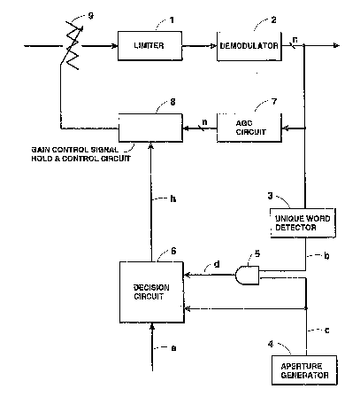
Referring to Figure 1 of the drawings, an AGC
. e~bodying the present invention i8 shown. The AGC is
:~ generally ~ade up of a limiter 1, a demodulator 2, a unique
word detector 3, an aperture generator 4, a gate 5, a
decision circuit 6, an AGC circuit 7, a gain control signal
hold and control circuit 8, and a variable attenuator 9.
Digitally modulated burst signals ~in Figure
3(a)) from remote earth stations are applied to the limiter
1 via the variable attenuator 9. The limiter 1 controls
:~ the power of the individual bur~t signals to a
~ ~.
.. . .
, ..
, . . :
, .. .. .
,' ' .
~ 5 - 2~3~35~
:
predetermined value. The limiter 1 has a linear range and
a saturation range, as shown in Figure 2 specifically.
The demodulator 2 demodulates the burst signals
having been controlled by the limiter 1 to a predetermined
power level, thereby producing an n-bit digital demodulated
,' signal.
The constant power level set up by the limiter 1
eliminates the delay of response particular to the
conventional closed loop type AGC and thereby stabilizes
the buildup of the leading edge of the burst signal.
The output signal of the demodulator 2 is also
- applied to the AGC circuit 7. In respon~e, the AGC circuit
7 calculates the power level of the input signal,
~' determines a difference between the calculated power level
'f 15 and a reference value (which will be detailed in the
following) and then outputs the resulting error signal,
i.e., a gain control ~ignal after filtering it. The gain
contrvl signal of the AG~ circuit 7 and the status decision
' signal (h) from the decision circuit 6 are fed to the gain
control signal hold and control circuit 8.
.'r.~ The reference value PR for the AGC circuit is set
as follows:
PR= - A ----- (1)
1~ (C/N) WOt-~
~,
whersin A in an input power to the limiter at a point A
- bordering the linear range and the saturation rang-~ as
shown in Figure 2, and (C/N)Wo~t is a C/N (carrier power to
noise power ratio~ which is the worst of (C/N)8 among
~ received burst signals from remote earth stations. A is
`~` determined by the characteristic of the limiter and (C/N)Wot8,
is set by the design of the satellite communication system.
Equation (l) is derived from the requisite that
the input power of the limiter at the worst ratio (C/N~Wot~"
be set at the input power A for the critical point. Since
the input power at the ratio (C/N) wot8t iS a sum of carrier
.
''~ 1` ~
~ .:
:
, ' ' :
203~3~5
;. ~
power C and noise power N, the requisite leads to the
following:
C + N = A .................. (2)
.~ 5
when equation (2) is rewritten in terms of the worst C/N,
i.e. (C/N)wO~
N (C/N)wo~lt ~ N = A ......... (3)
:. Replacement of N with PR and simple transformation in
equation (3) gives equation (1).
~ Once the limiter input at the (C/N)Wor~, among
.~! received burst signals from remote earth stations is set at
the critical point of the limiter, the received burst
~ signals from other remote earth stations goes beyond the
critical point and the limiter produces a constant level
which is coupled to the demodulator.
Thus, as will be explained later, the AGC control
signal is generated employing the reference value expressed
in equation (1) when a burst signal is absent while the AGC
control signal in the "no burst" period immediately before
the present "no burst" period is used when the burst signal
is present.
In a satellite communication system, the noise is
usually thermal noise and noise power N is expected to be
constant. However, the noise power changes with the gain
variation of a low-noi~e ampli~ier and that of a frequency
converter, each followed by the AGC control. The gain
variations ~hemselves do not affect ratio (C/N) because the
- signal power changes similarly with the noise change, but
the input power to the limiter at (C/N)Wo~ is different from
the value of the point A.
Therefore, the input noise power to the limiter
must be controlled to be constant to set the input power to
the limiter for (C/N)Wo~ at the above-mentioned critical
~'
,
,
.
:`
: . :
,
. .
' ' . .... . .
:
- 7 - 2 ~3 03~ 5
value. To achieve this, the noise power to the limiter may
be controlled to be constant when th~re is no burst signal.
The unique word detector 3 detects the candidates
of unique words from the output signals o~ the demodulator
2 and produces a unique-word candidate detection signal
- (b). The aperture generator 4 generates apertures (c) for
detecting unique words. The gate 5 is used to detect true
unique words and, when the detertion signal (b) exists
while the aperture (c) is open, produces a unique word
detection pulse (d). The unique word detection pulse (d)
does not appear when the detection signal (b) does not
~ exist while the aperture (c) is open. The decision circuit
`~ 6 outputs a status decision signal (h) in response to the
aperture (c), unique word detection pulse (d), as well as
a slot timing signal (e~ which is fed from the outside.
The status decision signal (h) remains at a low level from
the time when the aperture of the slot in which a unique
word was not detected ends to the time when the next slot
occurs. In the slots where unique words are detected, the
i 20 status decision signal (h~ goes high. A specific
aonstruction of the decision circuit ~ will be described in
detail later.
The hold and control circuit 8 continuously
delivers the gain control signal of the AGC circuit 7 to
::
the variable attenuator 9 as a gain control signal as long
as the ~tatus decision ~ignal (h) is in a low level, i.e.,
; from the time when the aperture of the slot where no unique
word~ were detected start to the time when the next slot
occur~. When the status decision signal (h) is in a high
level, i.e., in the slot where a unique word is detected,
the gain control signal hold and control circuit 8 retains
the gain of the variable attenuator 9 particular to the
previous slot where a unique word was not detected,
outputting the held value as a gain control signal. In
response to the gain control signal fed from the gain
control signal hold and control circuit 8, the variable
; attenuator 9 controls the factor of attenuation of the
:
, .
., .
.
. . - ' .
,
.. ..
'
- 2 0 3 ~
- 8
; input signal. ~ speci~ic construction of the gain control
signal hold and control circuit ~ will be described in
detail later.
A~ stated above, the illustrative embodiment
performs the AGC operation in the slot where a unique word
i8 not detected, i.e., where a burst signal does not exist
from the end of the aperture to the beginning o~ the next
slot, thereby maintaining the noise power constant. In the
slot where a unique word is ~etected, i.e., in the slot
where a burst signal exists, the illustrative embodiment
holds the gain of the variable attenuator 9 occurred in the
previous slot where a unique word was not detected and
~ causes the limiter 1 to maintain the power level of burst
; signals constant.
Figure 4 shows a specific construction of the
~ decision circuit 6. The decision circuit 6 has a set/reset
; flip-flop (5R F/F) 61, an inverting circuit 62, and a D
type flip-flop (D F/F~ 63. The unique word detection
pulses (d) and slot timing signal (e) are respectively
- 20 applied to the set (S) terminal and reset (R) terminal of
the SR F/F 61. In response, the SR F/F 61 produces a
signal (f) on an output (Q) thereof. The slot timing
signal (e) is generated by, for example, a slot timing
generating circuit, not shown, and adjusted to the timing
for a unique-word of receiving signals ~rom remote earth
stations. The output (f9 of the SR FIF 61, the slot timing
; signal (e) and the inverted signal (g) of the apertures (c)
are respectively applied to the data (D) terminal, set (S)
terminal and clock (CK) terminal of the D F/F 63. In
response, the D F/F 63 produces the status decision signal
(h). When the unique word detection pulse (d) is absent
-~ while the aperture (c) i9 open, the decision circuit 6
-~ determines that no burst signals are present, i.e., only
noise is present. As a result, the status decision signal
(h) remains in a low level from the time when the aperture
(c) is closed to the instant when the next slot timing
signal (e) arrives. On the other hand, when the unique
.
. .; .
':
~; ''i'' , ~ : ~
' " ~ ` ` :' . :
. - ~ '' ' '
9 2~303~
word detection pulse (d) appears while the aperture (c) is
. .
open, the d~cision circuit 6 determines that a burst signal
is present and maintains the status deci ion signal (h)
having gone high in response to the slot timing signal (e)
in the high level.
Referring to Figure 5, a specific constructions
of the gain control signal hold and control circuit 8 will
be described. The hold and control circuit 8 has an
inverting circuit 81, an AND gate 82, a latch circuit 83,
and a digital-to-analog (D/A) converter 84. The inverting
circuit 81 inverts the status decision signal (h) to
produce an inverted signal. An AGC sampling clock for
sampling the gain control signal of the AGC circuit 7 and
; the inverted signal of the status dPcision signal (h) are
fed to the AND gate 82, the inverted signal serving as an
enable signal. The latch circuit 83 latches the output of
the n-bit AGC circuit 7 with latch pulses which is fed from
the AND gate 82. In response, the latch circuit 83
-~ produces an n-bit output signal. The D/A converter 84
converts the n-bit output of the latch circuit 83 into an
analog signal to produce a control signal. While the
status decision signal (h) having gone high in response to
the slot timing signal is stlll in the high level, no latch
pulse is ~ed to the latch circuit 83. As a result, the
output of the AGC circuit 7 produced when the slot timing
appeared is held, so that the output of the gain control
signal holding circuit 8 is maintained constant. On the
other hand, when the status decision signal (h) goes low,
latch pulse are ~ed to the latch circuit 83 with the result
that the hold and control circuit 8 delivers the output of
the AGC circuit 7 directly without holding it. While the
hold and control circuit 8 has been described on the
assumption that the AGC circuit 7 is of a digital
processing typ~, it is similarly practicable with an analog
processing type AGC circuit if an A/D converter is
connected to the input of the latch circuit 83.
:",
` A
` .
.,
,
. .;
.~ .
. ` . .
. . .
- - lO - 2~303~
Figure 6 is a graph showing the relation between
Eb/No and BER particular to the coherent BPSK or QPsK
; modulation system. Eb/No is an energy-to-noise power
density ratio per bit and corresponds to C/N. In the
graph, P is representative of theoretical values determined
without error correction coding and by using the following
theoretical expression:
BER = - erfc ( ~Eb/No )
~ 10
!j where erfc is the err function and equal to
, .,
erfc (x) = 2 r e~Y dY .
~ Jx
In Figure 6, q is represenkative of the values
actually measured without error correction coding and by
using the AGC of the present invention. By contrast ~ is
20 representative of the values actually measured with a
conventional AGC and without error correction coding.
Represented by u is the graph of the theoretical values
derived ~rom simulation with error correction coding.
~ Further, v is representative of the values actually
,`'`! 25 measured with the AGC of the present invention with error
-` correction coding, while w is representative of the values
` actually measured with a conventional AGC with error
~` correction coding. While various different approaches are
available for error correction, the illustrative embodiment
30 uses convolutional code as error correcting code in
combination with VITERBI decoding. The constraint length
k and the coding rate R are selected to be 7 and 1/2,
respectively. In Figure 6, q is selected such ~hat the
..
linear region of the limiter 1 is reached when Eb/No is
35 approximately 0 dB.
By comparing q and ~, it will be seen that BER
~ associated with q degrades little in the relatively low
'~''
~ ' ' '.
. , ~ .
:`
2030`3~
. - 11
Eb/No range despite the u~e o~ the limiter 1 and begins to
degrade as Eb/No increases. Presumably, this is because in
the low Eb/No range not only the linearity is low but also
the influence of thermal noise is greater than that of non-
linearity.
f~ Nevertheless, BER corresponding to high Eb/No is
acceptable since earth stations for satellite communication
~; are so designed as to be operable even with BER
corresponding to low Eb/No. In addition, high Eb/No is
rarely attained for the actual channel reasons.
When a high BER characteristic is desired, use
may be made of the error correcting system. It is to be
noted that v, compared to w, degrades only slightly when
- Eb/No is high, and such a degree of degradation does not
matter at all, as stated earlier.
When such an error correcting system is used, an
error correcting decoder may be connected to the output of
the demodulator 2, in Figure 1.
In summary, in an AGC device for a demodulator
which receives burst signals time serially from a plurality
^ of station , the present invention allows a limiter to be
t` used by maintalning noise power constant at the input point
of the limiter. Even when a plurality of burst signals has
x a substantial difference in power, i.e., when the levels of
the burst signals fluctuate noticably, the limiter promote
stable dsmodulation without resorting to a longer preamble
at the head of a bursk signal.
-
, ~ r
~'
~'t=
'. '
'`.'
. .,~
"
'
' '.,.
;'.'.`.'
'.'`
. .
.,, `
'.`
.
`' ' .
., :
.~'~.`' ' ' '
.. `, : `
',',
. I
', _