Note: Descriptions are shown in the official language in which they were submitted.
SILICON WAFER TEMPERATURE MEASUREMENT BY OPTICAL
1 TRANSMISSION MONITORING
The present invention generally relates to a
method for accurately measuring the internal temperature
5 of semiconductor materials, and more particularly, to a
method and apparatus for accurately measuring the
internal temperature of semiconductor wafers undergoing
various forms of rapid thermal processing utilizing
nonintrusive optical techniques.
The field of semiconductor fabrication is an
important and increasingly complex technology which is
absolutely vital to the continued advancement of solid
state electronic device technology. The more common
semiconductor materials include silicon, germanium,
15 gallium arsenide, and among these, the material most
frequently used in semiconductor devices is silicon. The
wide range of semiconductors and the various electrical
properties associated with each of the semiconductor
materials provide circuit designers with much flexibility
20 in designing devices with varyir.g electrical properties.
This need to create semiconductor devices utilizing
various semiconductor materials in one pacXage has become
one of the principle problems involved in semiconductor
fabrication.
Today, the trend toward smaller semiconductor
device geometries has created an interest in the short
time, high temperature processing of silicon, examples of
these techniques include rapid thermal annealing (RTA), and
rapid thermal processing (RTP) of ion implanted layers. These
techniques involve using radiant heating to couple heat
energy into the silicon. In order to take advantage of these
techniques, it is necessary to measure and control the wafer
ltemperature versus time profile very accurately. Today most
commercial RTP systems use either thermocouples attached to
the wafer or pyrometers which are calibrated against
thermocouples to monitor the semiconductor processing
5 temperature.
The most straightforward way to measure sample
temperature in semiconductor processing is with a
thermocouple. This method works well when the wafer is
surrounded by an environment at the same temperature of
10 the wafer, so that the thermocouple is of the same
temperature as the semiconductor wafer sample. A second
well known technique is optical or infrared pyrometry.
This technique looks at the optical energy emitted by the
wafer in a certain wavelength region. This energy is
15 characteristic of the temperature. This method requires
knowledge of the wafer emissivity of the given radiation
wavelength and also requires that all windows between the
sample and the pyrometer be transparent at the
wavelengths of interest.
In rapid thermal processing the environment
surrounding the wafer is at many different temperatures,
and thus, if a thermocouple is to be used to measure the
temperature of the wafer, there must be good thermal
contact between the thermocouple and the wafer. A
25 persistent problem associated with the use of
thermocouples is the method used to bond the
thermocouples to the wafers. Poor thermal contact and
slow response times can limit accurate measurement of the
wafer transient and in some cases steady-state temperature.
Conventionally, holes are drilled into the wafer for
insertion of the thermocouple, the thermocouple is then
sealed in the hole with a ceramic cement. This process can
lintroduce impurities into the environment which can adversely
affect both the temperature sensor and the devices fabricated
in the wafer. Further, the desired thermal contact is not
easily reproduced using cement holes and the integrity of the
5 thermocouple can be jeopardized.
United States Patent No. 4,787,551 to Hoyt et
al. discloses a method of welding thermocouples to
silicon wafers for temperature monitoring in RTP thereby
avoiding the aforementioned problems. However, the
10 disclosed method requires that the thermocouple be welded
using TIG welding and/or electron-beam welding which is a
multistep process that requires time and skill to
successfully complete. In addition, there is a risk of
damage to each wafer that a thermocouple is welded to.
Optical pyrometers have been used in
engineeLing and science applications for a relatively
long period of time, and their operation and use are well
known in the above mentioned fields. Optical pyrometry
offers the major advantage of measuring the temperature
20 of a body without having to physically touch the body;
however, the pyrometry method also has certain definite
disadvantages associated with its use which make it
impractical to use. Optical pyrometry can give different
results depending on what emissivity is used, and extreme
25 care must be taken to avoid measuring radiation from the
heat lamps used in the RTP or RTA apparatus. Optical
pyrometry becomes even more difficult at low
temperatures, of 600 C to 700 C, since measurement of
longer wavelengths of radiation, longer than three microns,
are required and the longer wavelengths are severely
attenuated by the windows used to measure the emitted
radiation. This presents a severe problem when a quartz
walled chamber is used to contain a reactive gas species, as
lin epitaxial growth applications, as disclosed as an example
in U.S. Patent No. 4,544,418 to Gibbons, because quartz is
fairly opaque to wavelengths greater than 3 microns. In
addition, field oxides and polysilicon layers among other
5 things will effect the emissivity and transmission of a wafer
because of thin film interference effects. These effects can
easily affect optical pyrometer measurements by up to 50C.
The present invention provides for a method of
non-invasively measuring the temperature of a semiconductor
lO material at elevated temperatures in the range of 400C
to 800C. It is particularly useful in processes which
involve the rapid thermal processing or annealing of a
semiconductor. The method includes the steps of
generating a monochromatic beam of electromagnetic energy
15 with a predetermined wavelength; focusing the beam onto
the surface of a semiconductor material; measuring the
intensity of the beam, after transmittance of the beam
through the material, to generate an electrical signal,
wherein the signal is representative of the intensity of
20 the transmitted beam; and calculating the temperature of
the semiconductor as a function of the electrical signal
and the thickness of the semiconductive material.
This method of temperature measurement, by
optical transmission monitoring, provides a non-invasive
25 optical technique for the accurate and rapid measurement
of the absolute temperature of silicon wafers. The
method provides for routine temperature monitoring of the
silicon wafer in the temperature range of 400C to 800C,
with resolution on the order of one degree centigrade.
Since the method does not depend on the
temperature of anything but the wafer, it is particularly
well suited to non-thermal equilibrium environments such as
lthose encountered in rapid thermal processing (RTP) or rapid
thermal annealing (RTA) systems where the wafer is usually
heated by radiation from heat lamps. The method is also
particularly well suited for RTP systems because RTP systems
5often require the silicon wafer to be enclosed in a quartz
container. Since quartz is transparent at the wavelengths
that have been found to be useful in the present invention,
the optical monitoring can now be done from outside the
quartz container walls. In addition, the present invention
10 provides a method for compensating for the pattern coatings
that usually form on the surface of the silicon such as
silicon dioxide or polysilicon.
The present invention has a wide variety
applications where a high degree of accuracy is
15 absolutely necessary. The method provided by the present
invention can operate RTP or RTA systems with constant
temperature monitoring and with closed loop temperature
control with feedback. The method could also be applied
to any other environment, but would be most useful where
20 thermocouples could not be used because of corrosive
gases or because of a lack of a uniform temperature
surrounding the semiconductor. The present invention is
applicable to almost all semiconductors, such as gallium
arsenide, germanium, indium phosphide among others. The
25 wavelengths that are useful in the practice of the
present invention are different for different
semiconductors since each has different absorptive
properties.
The invention also includes a highly accurate
temperature measuring device for measuring elevated
temperatures in the range of 400C to 800C with an
accuracy of one degree centegrade. The temperature measuring
ldevice uses a thin silicon wafer positioned between a beam of
monochromatic electromagnetic energy and a photon detection
means. The photon detection means measures the intensity of
the transmitted beam. A display means indicates the
5temperature of the silicon wafer, as a function of the
thickness of the wafer and the intensity of the transmitted
beam.
Figure 1 is a graphic representation of
normalized transmission values versus temperature for
10 silicon wafers having a thickness of 450 ~m;
Figure 2 is a diagrammatic block diagram of the
apparatus for the wafer temperature measurement by optical
transmission monitoring utilizing a single wavelength light
source;
Figure 3 is a diagrammatic block diagram of the
apparatus for the wafer temperature measurement by
optical transmission monitoring utilizing multiple
wavelength light sources; and
Figure 4 is a graphic representation of
20 normalized transmission values versus temperature before
and after application of silicon-germanium epitaxial
layers.
GEN~RAL THEORY
The method of silicon wafer temperature
25 measurement by optical transmission monitoring is based
upon observing the transmission of light at a certain
wavelength through the silicon wafer. While a silicon
wafer is opaque to visible light, it is transparent to
certain infrared wavelengths. When photons of selected
30 wavelengths are directed to the silicon wafer, photons
with energies greater than the band gap energy, Eg, are
-7-
mostly absorbed while photons with energies less than Eg are
lmostly transmitted. Photons with energy greater than Eg are
mostly absorbed by the semiconductor because the energy of
the photons excites the electrons located in the valence band
of the semiconductor, and these excited electrons i'jump" into
5the empty states of the conduction band of the semiconductor.
The photons with less energy mostly pass through or are
transmitted because the energy they contain cannot excite the
electrons. In silicon, the change in absorption as the
photon energy changes through Eg is not very sharp, however,
10 because phonons are also often required for this absorption
process. A phonon is a lattice vibration. In general, the
larger the photon energy with respect to Eg is, the larger
the absorption is. This is one of the two physical
mechanisms by which radiant energy is absorbed, the second
15 mechanism is absorption by free carriers. In all
semiconductor materials there are a certain number of
free carriers, and these free carriers are able to absorb
energy without "jumping" from one band into another. As
the temperature of the semiconductor increases, the
20 number of free carriers increases, thus there is
increased absorption at higher temperatures.
Silicon as well as most of the other
semiconductors have an Eg that is directly dependent upon
temperature. As the temperature of the silicon wafer is
25 increased, the band gap energy decreases and the number
of free carriers increases, and when the temperature of
the silicon is decreased the band gap energy increases
and the number of free carriers decreases. Therefore, as
the temperature of the silicon wafer increases, less and less
photons are transmitted through the wafer because Eg has
decreased which means the photon energy is larger with
1 respect to Eg, and also means more free are carriers
available, both of which increase absorption.
Conversely, if the temperature of the silicon wafer
decreases, more and more photons are transmitted through
5 the wafer because Eg has increased which means
the photon energy is smaller with respect to Eg
transmitted, and also means there are fewer free carriers
available, both of which tends to decrease absorption.
Mathematically, the optical transmission, I, of
10 a silicon wafer is given by
I = i1i2e ( ) ~ (1)
where i1 is the transmission of the top silicon surface,
i2 is the transmission of the bottom silicon surface,
~(T) is the absorption coefficient of the semiconductor
at temperature T at the particular wavelength of
radiation used, and d is the wafer thickness. It is
important to note that multiple reflections through the
wafer and interference effects are ignored in the
practice of the present invention because of the
scattering caused by the rough surface and beam
divergence. Basically, i1 and i2 have little dependance
upon the temperature of the wafer compared to the
e (T)d term, therefore, the transmittance will be
approximately equal to e (T)d. The absorption coefficient
~(T) is a function of temperature, thus as the temperature
increases, ~(T) increases and as the temperature decreases,
~T) decreases. In addition, as the thickness of the wafer,
d, increases, the
transmission decreases and as the thickness decreases the
1 transmission increases. Therefore, if one knows the
thickness of a wafer, which is easily measured, one can
directly relate the optical transmission I to the
temperature of the silicon wafer.
The detected signal depends upon the incident
light power, optical alignment and other systematic
factors. To remove the dependence of the measurements on
these factors a normalized transmission ratio or value is
used. The normalized transmission I(T,d) is defined as
10 the ratio of the light transmitted at temperature T to
the light transmitted a room temperature To~ or for any
fixed temperature where the temperature is repeatable.
The normalized transmission I (T,d) will also not depend
upon surface reflectivity which may be effected by
surface layers such as field oxides or polysilocon
layers. Therefore, the normalized transmission is given
by
I (T,d) = e ~T)d = transmitted signal at temperature T (2)
e (To)d transmitted signal at temperature To
or
I (T,d) = e[~ (To)~ ~(T)]d
Constant factors such as laser or light power do not
enter into the expression for I given in equation (3).
DEVELOPMENT
Because of the scarcity of good data on the
optical properties of semiconductors at elevated
3o temperatures, the method which shall be explained
subsequently, is first calibrated against a known method
such as measuring transmission versus temperature in a
-10-
Eurnace enviLonment where a thcrmocouple can be used to
ldefine a known temperature, and thus develop a curve of
normalized transmission versus temperature. Once the
transmission versus temperature curve is derived for a
specific semiconductor, the system can be used in other
5operating environments wherein the temperature is to be
measured in the 400C to 800C range if silicon is the
semiconductor material to be measured. The transmission
does depend upon sample thickness d, thus if samples are
of different thickness one must either use a calibration
10 curve for that thickness, or else correct for the
different thickness using the well known e (T)d
relationship. Utilizing the result known in equation
(3~, the relationship between the normalized transmission
I(T,d) for two thicknesses d1 and d2 is given by
I(T,d ) = [I(T,d )]d2/dl (4)
Thus, if only o~e calibratio~ curve is done for a given
wavelength and thickness, one can, by utilizing equation
(4~, calculate I for a different thickness is of wafers
utilizing the same wavelength radiation.
As an example, if a wafer which has a thickness
of 200 microns has a normalized transmission equal to 0.8
at a certain temperature and wavelength, a wafer of the
same material that is 400 microns thick would have a
normalized transmission at the same temperature and
25 wavelength given by
I(T~d2) = [o 8~400/200
or
I(T,d2) = 0-64 . (6)
As was stated previollsly, this derivation depends on the fact
lthat the reflection at the wafer surface does not change very
much as the temperature changes. With silicon, from room
temperature to 700C, one would expect only a 2 percent
change in reflection in the 1.3 to 1.5 ~m wavelength range,
5making it a good approximation to assume that the reflectance
does not change with temperature.
The calibration of the method has been done for
a silicon wafer of 450 ~m at two different wavelengths of
radiation; namely, at 1.55~m and 1.30 ~m. The
lO calibration was done utilizing a thermocouple welded to
the wafer, as described in U.S. Patent No. 4,787,551, in
a rapid thermal processing reactor. The results are
shown in Figure 1, which may be used to determine the
temperature of the wafer when the normalized
15 transmittance is known. Also shown in Figure 1 is the
normalized transmission of a wafer of similar thickness
measured in a conventional furnace enviromnent where the
wafer temperature was measured by a thermocouple inserted
into the furnace tube. As is seen in Figure 1, there is
20 excellent agreement between the measurements. In the
following description of the method of the invention, a
complete description of how the transmittance values are
normalized is given.
Figure 1 illustrates the transmittance values
25 of a known silicon wafer. The values have been
normalized to cold transmittance values. A welded
thermocouple in the wafer was used for calibration. The
source frequencies had wave lengths of 1.55 ~m and 1.3
~m. The higher energy photons at 1.3 ~m have higher
absorption than those at 1.5 ~n at a given temperature.
The greatest accuracy for temperature measurement will
occur when the relative transmission is a strong function of
ltemperature. For example, near 750C, a 4 percent change in
transmission o~ the 1.55 ~m laser corresponds to only a
temperature change of approximately 1C. However, near
600C, to get 1C accuracy, a less than 1 percent change in
5the 1.55 ~m signal would have to be detected. While this is
easily done with fairly simple electronics, there is a
fundamental advantage of using the transmission at 1.3 ~m at
lower temperatures. At 600C, a 5 percent change in the
transmitted signal corresponds to about 1C, five times more
lO accurate than the 1.55 ~m signal of that temperature. This
illustrates that for accuracy, the highest photon energy
where a detectable transmitted signal is still received
should be selected. Further, below 500C, the change in the
1.55 ~m transmittance with temperature is f~irly small,
15 making this wavelength not a useful measure of temperature
below that threshold. However, the transmittance at 1.3 ~m
LS a strong function of temperature down to at least 400C.
From a practical point of view, it is found that the 1.3 ~m
and 1.55 ~m combination very useful for work anywhere between
20 400C to 800C, with a daily absolute accuracy within a few
degrees. The only adjustable parameter is the wafer
thickness, which of course is very easily measured.
OPERATION
Figure 2 illustrates the application of the
25 present invention to a basic RTP system. As illustrated,
a lamp-heated rapid thermal processing system is provided
with quartz walls for gas containment as used in the
description process disclosed in U.S. Patent No.
4,544,418. This configuration is also known as a limited
3o
reaction processing system. The apparatus indicated within
lthe dotted lines is a means for performing the temperature
measurement process while the remaining elements are part of
a conventional rapid thermal processing system. As was
stated previously, the transmission values shown in Figure 1
5are normalized transmission values. In order to remove the
effect of ambient light and electrical noise, a room
temperature or cold wafer temperature measurement should be
done first so the hot temperature measurements can be
normalized.
The rapid thermal processing system consists of
first and second water cooled reflectors 10 and 12 which
provide for the even heating of the silicon wafer 14
which is enclosed in a quartz tube 16. The heat energy
for the process is supplied by a series of heating lamps
15 18. For purposes of this illustration, it is assumed
that the wafer will be heated to a specific temperature,
which is exactly monitored and controlled. The optical
temperature detecting means of the present invention is
used to monitor the temperature of the wafer 14 and to
20 control the temperature of the wafer by adjusting the
output of the heating lamps 18.
The process begins by directing light energy
from a semiconductor laser 20 onto the silicon wafer 14
through an opening 21 in water cooled reflector 10. In
25 the embodiment used to generate the values represented in
Figure 1, the electromagnetlc energy supplied is at a
wavelength of either 1.55 ~m or 1.30 ~m and can be
supplied from other sources than a laser such as a light
emitting diode, LED, or a white light source; however, it
is important that whatever light source is utilized, the
beam must be monochromatic, typically having a 0.01 ~m
bandwidth. Whichever radiation source is utilized, some
-14-
~orm of modulation should be used for ease of detection of
lthe transmittance signal. The typical range of modulation of
the radiation is between 100 Hz and 100 KHz. In addition, if
a white light source is utilized, it must be filtered with a
monochromatic, diffraction grating or the like to be within a
5specific bandwidth. The light energy from the semiconductor
laser 20 is directed through a fiber optic element 22 onto a
lens 24. The fiber optic element 22 is not necessary if the
laser 20 can be lined up directly with the wafer 14. The
fiber optic element 22 is only utilized for convenience of
10 mounting the light source. The lens 24 is used to focus the
light energy directly onto the wafer 14. Once again the lens
24 is not absolutely necessary, but insures that the maximum
amount of radiation impinges upon the wafer 14.
Depending upon the temperature of the wafer 14,
15 a certain amount of light energy will be transmitted
through the wafer. The thickness of the wafer is already
known and thus is not a variable in the process.
Whatever light energy is transmitted through the wafer
14, it is collected by an optical detector 26. The
20 optical detector 26 converts the transmitted light energy
into an electric signal, which is normally measured in
volts. The voltage signal is proportional to the
transmitted light and is fed into a lock-in amplifier 28.
After amplification of the incoming signal, the lock-in
25 amplifier 28 is used to discriminate the signal of
interest from the stray signals that arise from any other
ambient optical interference, such as light from the heat
lamps 18, impinging upon the detector 26. When the rapid
thermal process is first started, the output of the
lock-in amplifier 28 is a first signal representative of
transmission I(T,d) when T is equal to To~ or the room
ltemperature. The output of the lock-in amplifier 28 when the
process is running is the first signal, representative o~ the
transmission I(T,d) when T is equal to whatever temperature
the wafer 14 has been elevated to. Thus, the values at room
5temperature and at operating temperature are substituted into
equation (2) and the normalized value is read from the
vertical scale of Figure 1 and the operating temperature is
determined. If the thickness of the wafer is different from
the one in Figure 1, equation (4) may be used to compensate
lO for the difference in transmission. The signal output from
the lock-in amplifier 28 is fed to an output display 32.
The output display 32 can be a computer which
is programmed to automatically implement equations (3)
and (4) or a display unit that displays the value of the
15 first signal on a calibrated scale to represent the
operating temperature. With a simple voltmeter type of
device a separate calibrated scale would be necessary for
each thickness and each type of semiconductor. Once the
temperature is known, the heat lamps can be manually
20 adjusted or~automatically adjusted through an automatic
control system utilizing the present invention in the
feedback loop.
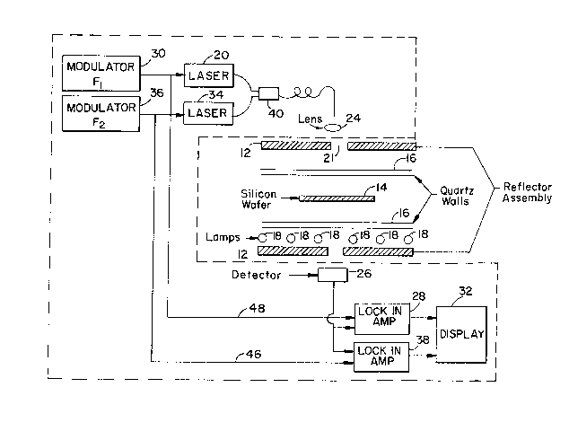
Figure 3, illustrates the present invention
with a two laser system. As was stated before, the
25 process or method is more efficient when two different
wavelengths of light are used. As indicated in the
figure, two lasers 20 and 34 are used, with two
modulators 30 and 36 producing two separate and distinct
driver frequencies, f1 and f2. Two lock-in amplifiers 28
and 38 are also used to separate out the values of f1 and
f2 after transmittance. While multiple frequencies are
-16-
advantageous for sensitivity, it is also desirable from a
lpractical point of view, to minimize the optical hardware
required, including the number of beam paths. Thus, an
optical coupler 40 is used which provides for the use of
multiple lasers on a common beam path. A single detector
526 is used to detect the combined signal, and a pair of
lock-in amplifiers 28 , 38 are used to separate the
various transmitted signals. The laser sources 20 and 34
are modulated at different frequencies fl~ f2 and
combined onto a common fiber 22 by means of the coupler
lO 40. This one fiber 22 is used to project the optical
signals through the wafer, and a single detector 26 is
used to generate a combined or superimposed first and
second signal. The first and second signals
representative of the transmittance values at the two
15 different wavelengths can be separated by using loc~-in
amplifiers 28 and 38, which are synchronized to the
desired modulation frequency by reference signals on
control loops 4~ and 48.
Field oxides, polysilicon layers, etc, will
20 effect the emissivity and transmission of a wafer because
of thin film interference effects. These effects can
easily effect optical pyrometer measurements by 50C.
While such layers will also effect optical transmission,
they are not a function of temperature. Therefore, the
25 effect of these layers may be automatically taken care of
by normalizing the operating temperature signal to the
room temperature signal.
Recently there has been a large interest in
silicon-germanium epitaxial layers on silicon for devices
such as heterojunction bipolar transistors (HBT). These
layers have smaller bandgaps than that of silicon, and
might be thought to strongly affect the transmission,
making temperature measurement based on optical
transmission using silicon substrate parameters impossible.
l However, relevant thicknesses and germanium concentrations
for a ~aT will probably involve roughly 20 percent germanium
in 50 mm layers. In order to determine the effect of such a
layer on the accuracy of the present invention, a
5 silicon-germanium epitaxial layer was grown on a silicon
wafer, and the temperature of the wafer was tested with both
the present invention and with a welded thermocouple.
Figure 5 illustrates the transmission at 1.3
and 1.55 ~m both before and after the silicon-germanium
lO growth. The squares with the dots in the center
represent the 1.55 ~m wavelength transmission with a
welded thermocouple in a RTP process, the black diamonds
represent a 1.55 ~m wavelength transmission with a
furnace calibration, and the solid black s~uares
represent a 1.3 ~m wavelength transmission with a welded
thermocouple in a RTP process. As can be seen from
Figure 5, the transmission values before and after are
virtually identical, and are within the accuracy of the
current apparatus. Thus for technologically relevant
layers of interest, the present invention may be used
with silicon-germanium layers without having to modify
the apparatus or the method in anyway.
3o