Note: Descriptions are shown in the official language in which they were submitted.
2 ~
1 BACKGROUND OF THE INVENTION
(a) Field of the Invention
The present invention relates to an optical
memory such as an optical disk and an optical card for
recording, reproducing and erasins information with
employment of laser light or the like, and also to an
information processing apparatus.
Also, the present invention relates to an
optical memory and an information processing apparatus
used only for reproducing information previously stored
therein.
(b) Description of the Related Arts
In an optical recording medium such as an
optical disk, laser light or the like is collected until
it reaches a diffraction limit thereof in order to record,
reproduce and erase information. As a result, the
information can be recorded on such optical recording
mediums at extremely high density.
Thus, such large capacity-memories have been
mainly developed as auxiliary memories for large-scale
computers.
On the other hand, small-sized portable computers
representative of, for instance, lap-top computers have
been marketed very recently. Floppy disks have been
2~3~2
1 presently utilized as typical changeable medium memories
fox small-sized computers. However, the memory capacity
of the typical floppy disk is rather small. A strong
demand has been currently made for such a high-density
memory with a changeable recording medium instead of the
floppy disk.
To accept such demands, various types of optical
memories have been proposed.
For instance, as to compactness, optical cards
with higher portabilities have been proposed. Although
an optical card has such merits that a higher portability
may be expected with a compact size and a large memory
capacity, there is a difficulty that the data transfer
speed thereof is very slower than that of a rotation
type optical disk, because both the data recording and
; reproducing operations are performed in a linear scanning.
To solve the above-described difficulty belonging to the
optical card, one invention has been made as JP-A-60-
79581. This invention is directed to a card in which a
rotation type recording medium sheet, for instance, an
optical disk having a thickness substantially equal to
a thickness of a conventional cash card. Since data
are recorded on the rotation type recording medium sheet
in this optical card, there is a particular advantage
that higher data transfer speed may be achieved, as
compared with that of the conventional optical card.
As a result, this invention can overcome the above-
described problem inherent to the conventional optical
2~3~
1 card, i.e., low data transfer speed, while other merits
such as better portability and easy handling of the
typical optical cards are maintained.
On the other hand, in the conventional optical
disk, this optical disk is mounted within the cartridge
case/ the shutter is opened/closed which is provided
on a portion of the case within the disk drive, and the
laser light is irradiated onto the disk. The reason
why such an optical disk is mounted within the cartridge
case, is to prevent dust from being attached on the
disk surface and also to realize easy mounting operations
by this cartridge case. However, generally speaking, a
thickness of a hard cartridge case is rather thick and
there is a drawback that a total weight of the cartridge
case becomes heavy. Therefore, there is a demand to
make the cartridge case thinner and lighter. Neverthe-
less, to make a ~hinner cartridge case, an optical disk
substrate having a typical thickness of 1.2 mm must be
made thinner. In general, when a thickness of a
substrate becomes thinner, an adverse influence caused
by a laser scattering (due to dust attached on the
substrate surface~ becomes greater. As a result, this
may cause, in turn, other various drawbacks that the
laser power during the recording operation is lowered
and read-out errors during the reproducing operation
may happen to occur. Consequently, the presently
available shutter type cartridge case can hardly prevent
dust problem. As one of dust preventing methods, a
2~3~2~
1 mechanism has been proposed in JP-A-64-25378 that dust
is collected by controlling air flows. However, there
is no clear description that such a dust preventing
method may be similarly applied to the above-described
thinner optical disk substrate. ~or instance, as
described in another publication, JP A 64-30087, the
following dust preventing idea has been proposed:
The optical disk is sealed within the cartridge case by
way of the shutter and the laser light is irradiated
through the cover glass formed on the cartridge case
onto the surface of the optical disk.
In accordance with the conventional dust
preventing ideas as described in JP-A-60-79581 and
JP-A-64-30087, to achieve the sufficient dust protection
with the thinner memory medium, the optical disk built
in the cartridge case must be highly sealed, or suf-
ficiently sealed within the cartridge case. To this
end, there exists a particular advantage that the laser
light is projected via the case cover onto the disk
surface, which is different from another conventional
system in which the laser light is directly irradiated
onto the disk surface.
When, as described above, the optical disk is
built in the cartridge case, this case is spatially
separated from the optical disk so that a space is neces-
sarily formed therebetween. Air is filled in this space
under normal use environment. On the other hand, in
case that a flexible thin optical disk as described in
-- 4
l JP-A-60-79581 and JP-A-64-30087 is employed so as to be
rotated within a case, space intervals between the
optical disk and case are continuously varied due to face
vi.brations of this optical disk, while rotating the
optical disk. In particular, since the face vibrations
of the mechanically flexible optical disk become great,
such great face vibrations may be suppressed by employing
the stabilizer plate as described plate as described in
JP-A-64-30087. However, it is very difficult that the
rotating optical disk never collide with the stabilizer
plate, but the rotating optical disk is set in close
proximate to the stabilizer plate under which an air
bearing effect may be established therebetween.
SUMMARY OF THE INVENTION
An object of the present invention is aimed
not to mitigate a face vibration occurring in a built-in
optical recording medium, particular to an optical disk
as in the above-described prior art, but to mitigate
an irregular fluctuation in an optical characteristic
such as reflectivity of the optical recording medium,
which is caused by the face vibration during recording,
reproducing, or erasing operation.
The present invention is to provide an optical
memory and an information processing apparatus, in which
while, as previously described, a memory is made thin,
a case is tightly sealed in order to su~ficiently realize
2~3~22
1 dust~proof property, and laser light is irradiated
through the case to a surface of an optical recording
medium such as an optical disk which is relatively
moved with respect to the case, for instance, in a
rotating form, whereby optical recording operations such
as data recording, reproducing, or data erasing are
stably performed.
BRIEF DESCRIPTION OF THE DRAWINGS
Fig. 1 schematically represents a construction
of an optical memory according to the present invention;
Figs. 2A and 2B are illustrations for showing
principle of fluctuation in reflectivity caused by
face vibrations;
Figs. 3, 4 and 22 represent the fluctuation in
reflectivity caused by face vibrations;
Figs. 5 to 11 are schematic diagrams for showing
constructions of an optical memory according to the
present invention;
Figs. 12 to 18 are schematic diagram for
representing constructions of antireflection films;
Fig. 19 is a graphic representation for showing
spectral reflectivity of a case having mixed antireflection
films;
Figs. 20, 21, 23A, and 23B are schematic
diagrams for showing a construction of a card-shaped
optical memory;
Fig. 22 is a characteristic diagram of the
~3~
1 card-shaped optical memory according to the present
invention;
Figs. 24A and 24B are schematic diagrms of
the optical head and optical disk, and also a control
diagram thereof, and,
Fig. 25 is a shcematic block diagram of an
inormation procesing apparatus.
DESCRIPTION OF THE PREFERRED EMBODIMENTS
An optical memory according to the present
invention is characterized by comprising a case, an
optical recording medium disposed within the case, and
an antireflection film. This optical recording medium
is movable within the case, and more specifically is
preferable to be rotatably stored within the case. Also,
the antireflection film is preferable to be employed on
at least one of the case and recording medium.
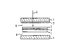
As represented in Fig. 1, features of the
present invention are as follows. In principle, the
optical memory has a supereme self-holding characteristic
and a better portability, and further environment
resistance, oilproof characteristic, chemical resistance.
A construction of the optical memory is made such that
an optical recording medium 3 is built in a pair of case
1 (including a cartridge form and a card shape) having
a transparent portion, which is relatively moved with
respect to this case 1, and an antireflection film or
coating 2. It should be noted that reference numeral 4
-- 7 --
.
~3~2~
l shown in Fig. 1 denotes a substrate of the optical
recording medium; reference numeral 5 indicates an
optical path; and reference numeral 6 represents an air
layer formed by the card and optical recording medium.
Although the antireflection films 2 have been formed
on both of an interior of the card and the optical
recording medium, this antireflection film may be formed
on only one member thereof. Alternatively, this anti-
~ reflection film may be formed on an exterior of the card.
An optical memory according to the present
invention, comprises: a case having a transparent portion
and made of a material having a self-holding charac-
tristic; an optical recording medium stored within this
case, for recording, reproducing and erasing information
by light illuminated through the transparent portion of
the case; and, an antireflection film provided on at
least one of the above-described case and optical
recording medium along a light path of the light, and
made of a material through which the light can easily
pass from the case and optical recording medium.
The optical recording medium records informa-
ti~n on a substrate having a holding characteristic and
plasticity by way of physical or chemical changes by the
light.
At least one of a dielectric film or metal
reflecting Iilm is preferably formed on the optical
recording medium.
The optical recording medium may preferably
- 8 -
2 ~ 2
1 record, reproduce and erase information thereon in such
a manner that irradiating light thereto causes a phase
change in an amorphous-crystal.
As the optical recording medium, a recording
medium capable of recording, reproducing and erasing
information thereon by utilizing a photo-electro-magnetic
effect, may be employed.
The optical recording medium may be relatively
moved with respect to the case within the case. Further-
more, it is preferable to rotate the optical recordingmedium with a substantially constant center axis inside
the case.
The optical recording medium may be such a
disk as a compact disk only reproducing information
which has previously been recorded.
Assuming now that a refractive index of the
transparent portion of the case is "nl", a refractive
index of a space between the case and the optical recording
medium built in this case is "nO", and a refractive inde~x
of a first layer constituting the optical recording
medium with respect to an incident direction of the light,
a refractive index "n3" of the antireflection film
; employed in the case of the optical memory may be prefer-
ably ~ , whereas a refractive index "n4" of the anti-
reflection film provided on the first layer of the optical
recording medium may be ~n2nO.
As the antireflection film, a condition of:
nh = (2m + 1)~/4 may be preferable, assuming now that a
g
2 ~
1 wavelength of light used for recording or reproducing
information is "~", a refractive index of the anti-
reflection film is "n", a film thickness is "h", and
"m" is an integer.
Also, the antireflection film may be formed by
at least two layers having different refrection indexes
with each other, made of dielectric films selected from
one of oxide, fluoride, sulfide and calcogens compound.
Further, the antireflection film may be
preferably constructed of a dielectric film made by
mixing at elast two sorts of oxide, fluoride, sulfide,
chloride and calcogens compound having different
refractive indexes.
This antireflection film may be preferably
lS made of a material having higher transmittance than that
of the above-described case and optical recording medium.
Also, the light transmittance may be selected
to be more than 80 percents.
The optical memory may employ therein at least
two recording mediums.
A size of the optical memory may be preferably
shaped in a card, and an outer size thereof is smaller
than 110 mm in a lateral direction thereof and smaller
than 80 mm in a transverse direction thereof. A thick-
ness of the optical memory may be preferably smallerthan 3 mm.
An optical memory according to the present
invention comprises a case having a transparent portion
-- 10 -- .
2 ~
1 and made of a material having a self-holding character-
istic~s; and an optical recording medium stored in this
case, for recoxding, reproducing and erasing information
by irradiating light via the transparent portion of the
case thereon, and has such a feature that the transparent
portion of the case is made of a material through which
the light can easily pass from the optical recording
medium.
Transmittance of this transparent portion is
preferably higher than 80 percents.
A description will now be made of this anti-
reflection film. The antireflection film must be designed
based upon a material of the case on which the anti-
reflection film is provided, and a material of the
optical recording medium. Accordingly, although various
materials may be selected, the large light transmittance
of the materia] in proxlmity to a wavelength of laser
light used for recording/reproducing information is
necessarily required. Preferably, the light transmittance
may be selected be higher than 80 percents, or more than
90 percents. As this antireflection film, both a single
layer antireflection film and a multi layer antireflection
film may be employed.
Materials capable of being used as the anti-
reflection film are represented in a list 1.
2 ~ 2 ~
List 1: Materials usable as an antireflection filmfluoride
GeF3, LaF3, MgF2, Na3AlF8, BaF2, SrF2, ThF4,
LiF2 / CaF2
nitride
SiN, AlN
oxide
Ce2' Fe23~ Cr23, A1203, In203, 2 3
' 2~ 23~ r2~ a205
sulfide
ZnS
Calcogemide compounds
ZnSe, PbTe
organic resin
ultraviolet curableresin, epoxy,
acrylic polycarbon
1 There are mainly inorganic compounds such as
fluoride, nitride, oxide, sulfide, calcogens compounds,
and organic coating materials such as an ultraviolet
curable resin (UV resin). These materials may be employed
as a monolayer condition or a multilayer condition.
A method for manufacturing this antireflection
film will now be explained.
Various sorts of materials listed in the list
1 are formed on the case and optical recording medium.
As the manufacturing methods, there are vacuum vapor
deposition process, sputtering process, applicating
- 12 -
2 ~ 2 ~
1 process, chemical plating process, electric casting
process, printing process and the like. Other manu-
facturing methods used for normal thin film materials
may be utilized.
The antireflection film must be designed so
as to be fitted to the refractive indexes of the case
and optical recording medium, as previously explained.
To this end, materials having the suitable reflection
index are required to be employed as the antireflection
film. Although the refractive indexes of the materials
listed in the list 1 may be fitted to that of the
antireflection film to some extent, the refractive index
of the antireflection film must be freely controlled
in order to precisely suppress the above-described
reflection fluctuations.
As a refractive index control method of the
antireflection film, it is desirable to employ such a
method for mixing more than two different sorts of
materials each having different refractive indexes with
each other so as to control these refractive indexes
to a predetermined refractive index. As the mixture
method, there are a method for setting a multi-simultaneous
vapor deposition or sputtering process, a vapor deposition
source and a sputter target as a mixture, and further a
method for mixing in a solution. In general, a refrac-
tive index "n" of a mixed antireflection film is given
by Lorentz-Lorentz~s formula:
- 13 -
2 ~
2 ~ai ni Ci/pi
n = _ _
~ai Ci/Pi
where ai = l/(ni2 + 2)
1 "ni" indicates a refractive index of a mixed material
"i"; "ci" is a weight rate; and "Pi" represents a
density.
In Fig. 5~ there is shown a construction of
an optical memory in which an antireflection film 2 is
provided only inside a case. Similarly, ~luctuation of
reflectivity could be suppressed within 8 percents by
highly adjusting the refractive index of the anti-
reflection film in this construction. It should be
noted that reference numeral 1 denotes a transparent
case; reference numeral 3 indicates a recording layer;
reference numeral 4 represents a substrate; reference
numeral 5 denotes an optical path; and reference numeral
6 represents a space.
Fig. 6 represents a construction of an optical
memory with employment of an opaque case 7. In this
construction, there is formed a window 8 (transparent
portion) in a portion of the case, upon which laser light
is incident, and an antireflection film 2 is provided
only on the transparent portion of the case. It should
be noted that reference numerals 3 to 6 are similar
to those of Fig. 5.
A design of a monolayer antireflection film
will now be described. Assuming now that a refractive
~ .
- 14 -
2~3~
1 i.ndex of ~he antireflection film is "n"; a thickness of
this film is "h" (~m); another reractive index of a
case or a laser light incident window (transparent portion
of the case) on which the antireflection film is formed
is "nl"; and another refractive index of a space between
the case and optical recording medium built in the case
is "nO", n = ~ is satisfied based upon an amplitude
condition of interference, or nh = (2m + 1)1/4 is
satisfied ~ased on a phase condition, where "m" denotes
an integer, and "~" represents a wavelength (~m) of
laser light used for recording/reproducing operations.
A similar designing idea may be applied to the anti-
reflection film employed in the optical recording medium.
Although a complex designing idea is required
1~ for a multilayer antireflection film a generic designing
policy for two layers and three layers will now be
explained.
The following two typical models are available
for a two-layer antireflection film having refractive
indexes of n2 and n3.
~/4(n3~ - ~/4(n2)/case (nl) model.
Symbol "~" represents a wavelength of laser
light. In this case, optical film thicknesses n22 and
n3h3 of the two-layer antireflection film are preferably
equal to ~/4. Symbols "h2" and "h3" are film thicknesses
of the antireflection film.
~/4(n3) - ~/2(n2)/case (nl~ model.
In this case, both of optical film thicknesses
- 15 -
~3~
1 n2h2 and n3h3 of the two-layer antireflection film are
equal to ~/4 and ~2, respectively.
In the three-layer antireflection film having
the refractive indexes n2, n3 and n4.
~ ~/4(n3) - ~/2(n23 - ~/4(n4)/case
It should be noted that n2 ~ n4 > n3. In this
case, n32nl = n42 must be satisfied and these refractive
indexes are e~ual to ~/4 = n3h3 and ~/4 = n4h4.
As the materials for the recording film of the
optical recording medium, materials such as metal films,
organic colors, calcogenide compounds, magnetic thin
films andinorganic chloride are preferable which respond
to light or heat produced by light irradiation. In
particular, a material where~an amorphous-crystal phase
change may happen to occur, and another material having
a rewritable capability by way of the photo-elec~ro-
magnetic effect may be preferable.
As previously described, the optical memories
provided with the antireflection film are advantages for
achieving the object of the present invention. An
apparatus for mitigating the fluctuation in the reflec-
tivity~caused by the face vibrations of the relevant
optical recording medium, according to a system of the
present invention, will now be described.
In an optical memory, both a focusing operation
for correctly collecting a laser beam onto a medium
plane and a tracking operation for precisely tracing the
laser beam onto a recording track are required while
- 16 -
i ,. , . ,. ,~ ~ ,. . .
2 ~ 2 ~
1 recording, reproducing or erasing data. To this end,
the light reflected from the medium plane is returned
to a detector and then a servo control is performed
that a condenser lens is fine-moved by an actuator or
the like in response to output values of the detectors.
Accordingly, if, as previously described, the
fluctuation in the reflectivity of the medium happens
to occur, a normal servo control can be hardly expected.
Therefore, there is a necessity to monitor such a
refrectivity fluctuation in order to suppress this
fluctuation in the system.
In an optical memory according to the present
invention, there are employed: a case having a transparent
portion and made of a material with a self-holding charac-
teristic; and an optical recording medium stored withinthe case, in which a recording layer Eor recording,
reproducing and erasing information by receiving light
irradiated through the transparent portion of the case
has been formed on a transparent substrate, the trans-
parent substrate is made of a material through which
the above-described light can more easily pass rather
than the transparent portion of the case.
Transmittance of this transparent portion
of the case is preferably higher than 80 percents.
In an optical memory according to the present
invention, there are employed: a case having a transparent
portion and made of a material with a self-holding
characteristic; and an optical recording medium stored
2~3~2~
1 within the case via an internal plane of this case and
an air layer, for recording, reproducing and erasing
information by receiving light irradiated through
the transparent portion of the case, at least one of
antireflection means, the reflectivity of which at a
boundary plane between the optical recording medium
and air layer becomes below 4 percents, and anti-
reflection means, the reflectivity of which at a boundary
plane between the transparent portion of the case and
air layer becomes lower than 4 percents is employed
within the optical path.
An information processing apparatus, according
to the present invention, is characterized by comprising
an optical head to perform at least: functioning to an
memory which includes an optical recording medium
rotatably disposed within a case having a transparent
portion, and an antireflection film formed on at least
one of said case and said optical recording mediumi
recording information on said optical recording medium
by irradiating light thereon through the transparent
portion of the case; reproducing the information which
has been recorded on said optical recording medium;
and, erasing the:information which has been recorded
on said optical recording medium.
A variation in reflectivity of light reflected
from the above-described optical recording medium is
preferably selected to be smaller than 5%. Furthermore,
it is preferable to employ a circuit for correcting the
2 ~ 2
1 variation in the reflectivity of the light reflected from
the optical recording medium.
An information processing apparatus according
to the present invention comprises:
an optical memory in which an optical recording
medium for optically recording, reproducing and erasing
information is movably stored within a case having a
transparent portion;
an optical head for recording the information
on the optical recording medium, for reproducing the
information from the optical recording medium and for
erasing the information recorded on the optical recording
medlum;
means for setting a variation in a reflecting
amount of light reflected from the optical recording
medium to lower than 5 percents;
means for driving the optical recording medium;
and,
: a drive circuit for controlling an operation
of the optical head and a rotation number of the drive
means.
This drive means corresponds to a spindIe motor,
flat motor, linear motor and ultrasonic actuator for
rotating or performing a parallel motion of the optical
recording medium with respect to the case.
The optical head preferably includes a semi-
conductor laser; a collimation lens, an object lens, a
focusing actuator, a photodiode, prisms, a mirror, a
-- 19 --
,
2~3~J~2~
1 tracking actuator, a 1/4~ plate and an opto-acoustic
element.
Both of the optical head and optical memory
employed in the information processing apparatus according
to the present invention may be used only for reproducing
operation.
Also, the information processing apparatus
accoxding to the present invention may include a circuit
for correcting fluctuation in reflectivity of the light
reflected from the optical recording medium, instead of
the means for lowering an amount of reflectivity of the
light reflected from the optical recording medium.
In an information recording method according
to the present invention, light is irradiated onto an
optical recording medium movably stored within a case
having a transparent portion and made of a material with
a self-holding characteristic via a transparent portion
of the case, whereby information is recorded, reproduced
and erased on and from the optical recording medium,
and also the light is irradiated through an antireflection
film on a light path of the light, which is formed on
at least one of the above-described case and optical
: recording medium, and is made of a material the trans-
mittance of which is higher than 80 percents.
In an information reproducing method according
to the present invention, light is irradiated onto an
optical recording medium movably stored within a case
having a transparent portion and made of a material with
- 20 -
2 ~ 2 ~
1 a self-holding characteristic via a transparent portion
of the case t whereby the formation previously recorded
on this optical recording medium is reproduced, the light
is irradiated on a light path of the light via an
antireflection film which is formed on at least one of
the case and optical recording medium and is made of a
material the transmittance of which is higher than 80
percents.
The antireflection film employed in the infor-
mation processing apparatus according to the presentinvention, is to prevent or suppress interference of
light caused by the air layer. The light interference
caused by this air layer becomes a noise with respect
to a signal. Accordingly, this antireflection film may
lS also be referred to as "a light interference suppressing
film".
Furthermore, this antireflection film may be
preferably formed on both of the case and recording
medium.
Also, this antireflection film may be made of
a transparent material, and may have a refractive index
different from that of the case and optical recording
medium.
Then, the case may be relatively moved with
respect to the optical recording medium in accordance
with the present invention. More specifically, the
optical recording medium may be rotatable within the
case.
- 21 -
1 Also, an optical memory according to the present
invention comprises:
~.. a cas.e having a transparent portion and made of
a material with a self-holding characteristic; and,
an optical recording medium rotatably stored
within the case via an internal plane of the case and an
air layer, for performing at least one of recording,
reproducing and erasing operations for information
by light irradiated .through the transparent portion of
the case, characterized in that a light interference
suppressing film for suppressing interference of said
light at the air layer is provided in a light path of
the light in at least one of the internal plane of the
case and a plane in contact with the air layer of the
optical recording medium.
In an optical memory according to the present
invention, comprising a case having a transparent portion
and made of a material with a self-holding character-
istic; and an optical recording medium stored whithin
the case, and relatively moved with respect to the case,
for reproducing and recording/reproducing information,
or recoridng/reproducing/erasing the info~mation by liyht
: irradiated through the transparent portion of the case,
a thin film having a refractive index different from that
of sa.id case is formed on at least a side plane of the
case in a light path of said light of both said case
and optical recording medium, and also a thin film having
a refractive index different from that of a transparent
- 22 -
2 ~ 2 ~
1 substrate to constitute said optical recording medium
or that of a transparent thin film provided on an
outermost layer is formed on said substrate or outermost
layer thin film.
Further, in an optical memory according to the
present invention, comprising a case having a transparent
portion and made of a material with a self-holding
characteristic; and an optical recording medium stored
. within the case, and relatively moved with respect to
the case, for reproducing and recording/reproducing
information, or recording/reproducing/erasing the infor-
mation by light irradiated through the transparent portion
of the case, a thin film having transmittance greater
than that of said case is formed on at least one side
plane of the case in an optical path of the light of
both the case and optical recording medium, and also a
thin film having transmittance greater than that of a
transparent substrate to constitute said optical recording
medium, or that of a thin film provided on an outermost
layer is formed on said transparent substrate or thin
film of the outermost layer.
In the optical memory according to the present
invention, comprising a case having a transparent portion
and made of a material with a self-holding characteristic;
and an optical recording medium stored via an air layer
within the case, and relatively moved with respect to
the case, for reproducing and recording/reproducing
information, or recording/reproducing/erasing the
- 23 -
2 ~
1 information by light irradiated through the transparent
portion of the case, a thin film having a refractive
index different from that of said case is formed on at
least a side plane of the case in a light path of said
light of both said case and optical recording medium so
as to set reflectivity at a boundary plane with said
air layer to be lower than 4%, and also a thin film
having a refractive index diferent from that of a
. transparent substrate to constitute said optical recording
medium or that a transparent thin film provided on an
outermost layer is formed on said substrate or outermost
layer thin film.
An information processing apparatus according
to the present invention comprises:
an optical memory in which an optical recording
medium for optically recording, reproducing, or erasing
information is movably stored within a case having a
transparent portion;
an optical head for recording, reproducing,
or erasing the information on said recording medium;
means for setting a variation in a reflection
amount of light to be lower than 5%, which is projected
from said optical head and reflected from said optical
recording medium;
means for driving said optical recording
medium; and,
a drive circuit for controlling both operations
of said optical head and a rotation number of said drive
- 24 -
2~3~s~
1 means.
An information processing apparatus according
to the present invention comprises:
an optical memory in which an optical recording
medium for optically recording, reproducing, or erasing
information is movably stored within a case having a
transparent portion;
an optical head for recording, reproducing,
or erasing the information on said recording medium;
correcting means for correcting a variation
in a reflection amount of light to be lower than 5%,
which is projected from said optical head and reflected
from said optical recording medium;
means for driving said optical recording medium;
lS and,
a drive circuit for controlling both operations
of said optical head and a rotation number of said drive
means.
Also, an optical memory, according to the
present invention, comprises an optical recording medium
rotatably disposed within a case; and, a film for sup-
pressing interference of light occurring in an air layer
formed between the case and the optical recording medium.
In this optical memory, the interference suppressing
film is preferable to be provided on at least one of a
plane between the air layer of the case and this sup-
pressing film, and also another plane between the air
layer of the recording medium and this suppressing film.
2 ~
1 Also, the refraction index of the case is preferably
different from that of the optical recording medium.
In accordance with the present invention,
the antireflection films provided with the case and
optical recording medium have effects to reduce the
variation in the reflectivity which is caused by the
optical recording medium built in the case when being
relatively moved with respect to the case. Further,
the information is recorded, reproduced and erased by the
information processing apparatus including the correcting
circuit for monitoring the variations in the reflectivity
of the medium, so that the stable recording and repro~
ducing operations with the small variation of the
re~lectivity can be realized.
Irregular variations in the optical charac-
teristics such as reflectivity caused by the face
vibrations of the optical recording medium movable within
the case during the recording, reproducing, or erasing
operations will now be described.
In Figs. 2a and 2b, there are shown the varia-
tions in the reflectivity caused by the face vibrations.
To achieve a better data transfer speed than that of
the presently available floppy disk, an optical memory
must be designed such that assuming now that a diameter
of an optical disk 4 built in the optical memory is
selected to be 2 inches (approximately 50 mm), for
instance, this optical disk 4 must be rotated at a
rotating speed on the order of 3600 rpm. When the optical
- 26 -
2 ~ 7, ~
l disk 4 is rotated at such a high speed within the case
1 under substantially sealed condition, a pressure
difference may occur within the case l due to the face
that a velocity difference may exist between an inner
periphery and an outer periphery of the disk 4. Then
this pressure difference may induce the face vibrations
of the optical disk. There are other face vibrations
caused by center vibrations of the spindle for driving
the optical disk. As described above, when the optical
disk is rotated within the case, the face vibrations
may occur. Accordingly, this may cause an interval
between the case and optical disk to be continuously,
irregularly varied. Fig. 2a shows such a condition
that the optical disk 4 is positioned in close proximity
to the case l, wehreas Fig. 2b shows such a condition
that the optical disk 4 is most separated from the
case 1. Laser light 5 incident on the case perpendicular
to the case (not that an incident angle thereof has been
changed for the sake of convenience) produces one reflec-
tion light 5a which has reflected at a boundary planebetween the case and a space 6 within the case, and the
other reflection light 5b which has reflected at a
boundary plane between the optical disk 4 and the space
6. In the figures, both the reflection light at the
surface of the case 1 and the reflection light come
from the inside of the optical disk 4 containing the
data have been omitted. Considering now a case shown in
Fig. 2a where an interference condition for strengthening
- 27 -
2 ~ 2
1 the reflection light 5a and 5b with each other is
satisfied, and a case shown in Fig. 2b where an inter-
ference condition for weakening the reflection light 5a
and 5b with each other is satisfied, since the inter-
ference condition is continuously changed due to theface vibrations of the optical disk, the reflection
light 5a may be strengthened, or weakened with the
reflection light 5b. This fact may cause noise when a
variation in the reflectivity during the recording and
reproducing operations of the optical disk is detected.
Accordingly, if both the reflection light 5a and 5b is
reduced, the overall variation of the reflectivity may
be lowered.
In Fig. 3, there is shown a variation in
reflectivity when an optical memory is reproduced. An
amount of face vibrations produced while the optical
recording medium (in this case, an optical disk) built
in the optical memory was rotated within 1 rotation,
was 10 ~m at maximum. At this time, the variation in
the reflectivity became 22% at maximum, under which the
normal recording and reproducing operations could not be
realized. Accordingly, to achieve the stable recording
and reproducing operations by irradiating the laser
light via the case onto the optical recording medium
built in the case, the fluctuation in the reflectivity
caused by the face vibration of the optical recording
medium must be solved. To this end, the optical memory
according to the present invention includes such a
- 28 -
~3~
1 construction capable of mitigating the fluctuation in
the reflectivity.
Fig. 4 represents fluctuation in reflectivity
when an antireflection film has been employed in the
optical memory shown in Fig. 3. The fluctuation in the
reflectivity could be suppressed below 5%, as compared
with that of Fig. 3.
This implies that since the antireflection
films are provided with the case and optical recording
medium at a side of a laser incident reflection, the
reflection light 5a and 5b shown in Figs. 2a and 2b
are attenuated. Precisely speaking, to attenuate the
reflection light reflected from a surface of the case,
which is not represented in Figs. 2a and 2b, another
antireflection film may also be provided on the case
surface. However, even if no such an antireflection
film is provided on the case surface, there is no practical
problem.
In other words, according to the optical memory
of the present invention, providing the antireflection
films or coatings enables' the reflectivity fluctuation
during the recording/reproducing operations to be
mitigated even when the face vibrations of the optical
recording medium may happen to occur. An information
processing apparatus according to the present invention
can achieve stable recording and reproducing operations
by correcting the reflectivity fluctuation by a correcting
circuit and the like.
- 29 -
2~3~2~
1 The optical memory and information processing
apparatus according to the present invention, may
mitigate the fluctuation in the reflectivity caused by
the face vibrations due to movement of the optical
recording ~edium built in the case, and also may realize
a stable optical recording characteristic of the optical
memory.
In accordance within pre~erred embodiments, the
present invention has been embodied as an optical disk
which is a typical example of the optical recording medium.
(Embodiment 1)
Fig. 7 represents such a construction that
antireflection films 2a and 2b are provided on a case and
an optical recording medium. Inside the case 1 having
a thlckness of 2 mm and made of an acrylic resin, the
antireflection film 2a made of MgF2, having a thickness
of 16 mm, was formed by the sputtering process. Further-
more, the antireflection film 2b made of CeO2, having
a thickness of 100 nm, was formed by the sputtering
process on a naphthacyanine organic dye recording film
.
3 which has been coated on a glass substrate 4 forming an
Au reflection film 10. In accordance with this preferred
embodiments, fluctuation in reflectivity was within 5~
while the optical disk built in the optical memory was
rotated, and the stable recording/reproducing characteristic
- 30 -
2~3~2
1 could be achieved by utilizing a semiconductor laser
having a wavelength of 830 nm. Also, as a secondary
effect, a near ultraviolet radiation was shielded by
the case and therefore the environment resistance of
the organic recording medium could be improved. It
should be noted that reference numeral 5 indicates a
light path and reference numeral 6 denotes a space.
tEmbodiment 2)
In Fig. 8 r there is shown a construction that
the antireflection films 2a and 2b are provided on a case
and an optical recording medium. A transparent acrylic
resin window 8 upon which laser light is incident was
formed in a case 7 made of an opaque polystyrence
resin and having a thickness of 2 mm, and then the anti-
reflection film 2a made of MaF2, having a thicknessof 160 nm was formed by the sputtering process. The
optical disk built in the optical memory was so con-
structed that an Au reflection film 10 having a thickness
of 100 nm, a ZnS dielectric film 11 having a thickness
of 70 nm, the above-described In3SbTe2 ternary compound
recording film 12 having a thickness of 30 nm, a ZnS di-
electric film having a thickness of 70 nm, and also an SiO2
antireflection film 2b having a thickness of 140 nm were
successively formed on the glass substrate 4 by way of
the sputtexing process. In accordance with this preferred
embodiment, while rotating the optical disk built in
the optical memory at a rotation speed of 3600 rpm by
- 31 -
% ~
l employing a semiconductor laser having a wavelength
of 830 nm, the fluctuation in the reflectivity was
within 5%, stable recording/reproducing/erasing
characteristics with higher C/N could be realized, and
furthermore, the overwrite could be achieved. It should
be noted that reference numeral 5 indicates a light path
and reference numeral 6 denotes a space.
(Embodiment 3)
Fig. 9 shows such a construction that the anti-
reflection films 2a and 2b are formed on a case and an
optical recording medium. Inside a case l having a thick-
ness of 2 mm and made of a transparent acrylic resin,
the antireflection film 2a made of MgF2, having a thick-
ness of 160 nm was formed by the sputtering process.
An optical disk built in the optical memory was so
constructed that an Al dielectric film ll having a
thickness of lO0 nm, a TbFeCo Magneto-optical recording
film 13 having a thickness of 50 nm, an AlN dielectric
film having a thickness of lO0 nm, an SiO2 antireflec-
tion film 2b having a thickenss of 140 nm were suc-
cessively formed on the glass substrate 4 by the
sputtering process. By using a semiconductor laser 5c
having a wavelength of 830 nm, which has been linear-
polarized by an analyzer, the photo-electro-magnetic
disk built-in the optical memory according to this prefer-
red embodiment is rotated a rotating speed of 3600 rpm,
so that the fluctuation in the reflectivity was within
- 32 -
2~3~2~
1 1% and the stable recording, reproducing and erasing
characteristics could be realized. From these condi-
tions, it could be recognized that the present invention
also has a particular advantage in an optical memory
with employment of a Magneto-optical recording disk
the reflectivity of which is not directly detected.
It should be noted that reference numeral 6 indicates a
space.
(Embodiment 4)
In Fig. 10, there is shown an optical memory
according to another preferred embodiment, in which an
Na3AlF6 antireflection film 2a having a thickness of
160 nm has been formed by the vacuum vapor deposition
on a transparent acrylic resin window 8 which was formed
at a portion of a polystyren resin case 7 having a
thickness of 2 mm. Reference numeral 14 indicates an
Al layer (compact disk layer) having a thickness of
100 nm on which data have been previously recorded;
reference numeral 4 indicates a glass substrate; and
reference numeral 2b denotes a ZnS antireflection film
having a thickness of 150 nm. When the optical disk buiIt
in this optical memory was rotated at a rotation number
of 600 rpm, the stably reproduced signal with small
fluctuation could be produced. It should be noted that
reference numeral 5 indicates a light path and reference
numeral 6 represents a space.
- 33 -
2 ~ 2 ~
1 (Embodiment 5)
Fi~s~ lla and llb represent a construction
of an optical memory according to one preferred embodiment
of the present invention, in which a card-shaped memory
is built in a polystyrene resin case 7 having a thick-
ness of 0.2 mm. Fig. llb is a cross-sectional view taken
along a line A - A' shown in Fig. lla. As the construc-
tion of the built optical card, the constructions
described in Embodiments 1 to 4 may be employed. A
eature of this preferred embodiment is such that a
card-shaped memory 15 is driven within the case in a
translation mode 18. This translation drive may be
realized by magnetically connecting a magnet hub 16
(not shown) employed therein to a drive apparatus. Laser
light 5 is irradiated onto a surface of the card-shaped
memory 15 via a transparent acrylic window 8 which has
been formed on a portion of the case, so as to record/
reproduce data thereon/therefrom. A high speed data
accessing operation may be realized by the translation
20~ movement according to this preferred embodiment. Also
in this translation movement, both an MgF2 antireflection
film 2a and a CeO2 antireflection film 2b have an effect
to mitigate the reflectivity fluctuation. It should
be noted that reference numeral 4 indicates a substrate;
reference numeral 3 denotes a recording film; reference
numeral 17 represents a recording unit; and reference
numeral 19 shows a cadmium layer.
- 34 -
1 (Embodiment 6)
Figs. 12 to 15 represent structures of anti-
reflection films according to preferred embodiments
provided on the optical recording mediums. The anti-
reflection film 2 was provided at an incidence side oflaser light 5 for the optical recording medium. In the
structure shown in Fig. 12, ZnS, ZrO2 and TaO5 monolayer
antireflection layers represent particular advantages.
Similarly, in the structure shown in Fig. 13, SiO2/ZnS,
and CeO2/Y2O3 two-layer antireflection films own
particular advantages. In the structure shown in Fig. 14,
a ZnS/MgF2/SiO three-layer antireflection film has a
particular advantage. In a construction of a multilayer
antireflection film larger than the three-layer anti-
reflection film, as shown in Fig. 15, such a construc-
tion that a 3-layer period of ZnS/MgF2/SiO is stacked
by 10 periods represents a particular advantage.
(~mbodiment 7)
Figs. 16 to 18 represent structures of anti-
reflection films 2 according to preferred embodimentsof the present invention, employed in the case 1. In
the structure shown in Fig. 16, MgF2, CaF2, BaF2, ThF4
and LiF monolayer antireflection films own particular
advantages. In the structure shown in Fig. 17, MgF2/ZnS
and CaF2/Y2O3 two-layer antireflection films have
particular advantages. In the structure of the multi-
layer antireflection film higher than the two-layer
- 35 -
2 ~
1 antireflection film such a construction that an
LaF2/MgF2/SiO three-layer period is stacked by 5 periods
has a particular advantage.
(Embodiment 8)
As represented in Embodiments 6 to 7, the
structures of the antireflection films own particular
effects by stacking substances each having a different
refractive index. In accordance with this preferred
embodiment, a mixture film is mode of substrances having
different refractive indexes with each other as an
antireflection film. The antireflection film to be formed
on an acrylc resin case was fabricated by the vacuum
vapor deposition process with employment of a vapor source
A by mixing ZrO2 with MgF2. Fig. 19 graphically represents
an antireflectio~ effect achieved by this preferred
embodiment.
Fig. 19(a) represents spectral reflectivity of
a surface of an acrylic resin case having no antireflec-
tion film; Fig. l9(b) indicates spectral reflectivity of
a case having ZrO2 and MgF2 two-layer antireflection
films; and, Fig. l9(c) denotes spectral reflectivity of
a case employing the mixed antireflection film according
to this preferred embodiment. From the reflectivity
characteristics shown in Fig. 19, it may be understood
that the mixed antireflection film according to this
preferred embodiment has the best advantages.
- 36 -
1 (Embodiment 9)
Figs. 20A and 20B represent application
examples of the optical memory according to the present
invention. As shown in Fig. 20A, this application
example is constructed of a transparent card-shaped case
20 having a thickness of 0.5 mm and made of pol~sulfone;
an optical disk 21 built therein having a diameter of
130 mm; a stainless hub 22 fixed with an external drive
apparatus for rotating the optical disk 21; a laser
projection window 23 made of polycarbon, for projecting
the laser light so as to externally record, erase and
reproduce; and a stainless sliding type shutter 24 for
dust-proofing the laser projection window 23 and fixing
hub 22. This card has a thickness of 1.5 mm, a lateral
length of 85 mm and a transverse length of 53 mm.
Fig. 20B is a sectional view, take along a line A-A'
shown in Fig. 20A. As represented in this sectional
view, the optical disk 22 has a space defined between
the card-shaped case 20 and this disk 22. However, the
optical disk 22 may be in contact with the case face
during the rotation of the optical disk 22.
In Fig. 21, there are shown a detailed con-
struction of the optical disk built in the card-shaped
case and also a positional relationship of this optical
disk in the sectional direction. Reference numeral 20
shown in Fig. 21 indicates a card-shaped case; reference
numeral 21 indicates an optical disk; reference numeral
23 represents a laser projection window; reference
- 37 -
2~3~,2
1 numerals 2a and 2b indicate an MgF2 antireflection film
having a thickness of 160 nm which has been formed on
the card-shaped case and laser projection window, and
another ZrO2 antireflection film 2b having a thickness
of 100 nm provided on the disk 21 in the laser projection
direction, respectively, reference numeral 3 indicates
an In3SbTe2 ternary compound recording film having a
thickness of 30 nm (note that this film may be selected
from not only In3SbTe2, but also other materials opened
in JP~A-No. 63-251290) capable of recording/erasing
information by irradiating laser light therein, whereby
amolphous-crystal phase change occurs; reference numeral
4 denotes a stainless circular substrate having a thick-
ness of 0.03 mm; reference numeral 25 indicates an optical
system such as an object lens for collecting the laser
light 5 onto the optical disk 21; and reference numeral
6 denotes an air layer necessarily formed between the
card shaped case and optical disk.
In Fig. 22, there is shown fluctuation in
reproduced signals (corresponding to the reflectivity
of the card) derived from a mirror unit for focus-
controlling the laser beam and servo-controlling the
tracking operation when the optical disk employed within
the card is rotated at a rotation speed 3600 rpm. As
apparent from Fig. 22, it can be seen that the reflec-
tivity fluctuation in the card according to the present
invention is considerably reduced. To achieve the stable
focusing and tracking operations of the laser light on
- 38 -
2 ~ 2 ~
1 the optical recordiny medium, it may be easily understood
that the fluctuation in the reflectivity of the mirror
unit is reduced as small as possible. Also, in the
card according to the present invention, the recorded
signal could be reproduced under condition that C/N
corresponds to 50 dB. As previously stated, it could
be proved that setting the antireflection films 2a
and 2b must be required in the card in which the rotation
type optical disk has been formed. Furthermore, as
shown in Fig. 23, in accordance with the present appli-
cation example, the data transfer speed can be easily
improved by employing two sheets of the built-in optical
disk and by over-writing the data in the parallel and
simultaneous fashion, and recording/reproducing the
data in the parallel form. It should be noted that
reference numerals employed in Fig. 23 are the same as
those employed in Fig. 20.
Figs. 24A, 24B and 25 represent an information
processing apparatus according to a preferred embodiment
of the present invention. As described in the specifi-
cation, a feature of this information processing
apparatus is to employ a mechanism for mitigating the
fluctuation in the reflectivity of the optical memory
caused when the recording and reproducing operations
are carried out. Fig. 24A represents a construction of
an optical head employed in this information processing
apparatus. This optical head is arranged by an object
lens 25 with an actuator for focusing the laser light
- 39 -
2 ~
1 onto the optical recordiny medium and also for tracking
this laser light; a 1/4 wavelength plate 27; a polarized
beam splitter 28; an opto-acoustic element 29; a
Foucault prism 30; a condenser lens 31; a position
sensor 32; a beam shaping prism 33; a collimeter lens
34; a laser diode 35; and an operational amplifier 36.
When the light returned from the optical memory medium
26 is returned to the polarized beam splitter 28, an
opto-acoustic voltage proportion to an amount of the
returning light is outputted from the opto-acoustic
element 29. This output voltage is differential-detected
by the operational amplifier 36 so as to control the
laser power output of the laser diode 35 via a servo
loop 37. It is so designed that the reflectivity fluctua-
tion caused from the optical memory is continuouslymitigated by the servo control loop defined by 29 to 35.
It shoudl be, however, designed that the laser power
control servo system is not operative during the record-
ing and reproducing operations of the optical memory,
as shown in Fig. 24B. This is because the reflectivity
fluctuation during the data reproducing operation is
distinguishable from the change in the reflection amount
caused when the laser power is increased during the
recording operation. As a consequence, as represented
in Fig. 24B, the laser power control servo system is
operated only when both the focusing and tracking servo
systems are in an operative condition. As the opto-
acoustic element, a pyroelectric substance such as
.
- 40 -
2 ~ 2 ~
1 PZT, LiNbO3 and ZnO may be used.
Fig. 25 shows a schematic block diagram of
one arrangement of the information processing apparatus
is constructed of an optical memory 38 including an
optical disk 3; an optical head 39; a motor 40 for
rotating the opti.cal disk; a drive circuit 41 for
driving both the optical head and motor; a processor
43 for recording the data, for processing the reproduced
data, and for managing output/input of the data; input
means 44 such as a keyboard; and, output means 42 such
as a CRT. It should be noted that the optical memory
38 is provided within this information processing ap-
paratus and has flexibi.lity.
- 41 -