Note: Descriptions are shown in the official language in which they were submitted.
~03~
DAT DRIVE/CONTROLLER INTERFACE
. ~: .
:- 1 This ls a continuation of application Serial No.
07/465,726, filed January 17, 1990.
, BACKGROUND OF THE INVENTION
The disclosed invention is directed generally to
computer storage digital audio tape (DAT) drives, and more
particularly is directed to an interface between a DAT
: drive and an associated controller.
Digital audio tape tDAT) technology, which was
developed for audio programming as defined in the DAT
Conference Standard, DIGITAL AUDIO TAPE RECORDER, June
1987, published by the Electronic Industries Association
of Japan, has been adapted for storage of computer data.
An example of a format for the storage of computer data
utilizing DAT technology is the American National Stan-
dard~ Institute (ANSI) Digital Data Storage (DDS) stan-
dard, presently in draft form ("PROPOSED AMERICAN NATIONAL
STANDARD ~ELICAL-SCAN DIGITAL COMPUTER TAPE CARTRIDGE 381
mm (0.150 in~ FOR INFORMATION INTERCHANGE," ASC X3 Project
No. 668-D). :
The characteristics that have made DAT technology
attractive for computer data storage include high capaci-
ty, high transfer rate capability, relatively small media
size and low media cost, and the adaptability of DAT
. technology to conform with personal computer storage
:`` :
. ~ .
', '
.? ' , : -: ' . . . :
', `"~`, ' . . ', ' ` ' ' ' ' ' ' :, . ' , " . , ' ' ' '
~ ~t ~
1 device form factors including th~ 5-l/4 and 3-1/2 inch forms.
The use of DAT technology for storage of computer
data can be achieved by application of a data storage
format, such as the above referenced ANSI DDS standard, to
the DAT Conference audio standard. In particular, the DAT
audio standard physical track format is retained, but the
contents of the information stored in the tracks is in
accordance with the computer data storage format.
DAT technology was developed primarily for audio
~' applications, and therefore an important consideration
with the use of DAT technology for computer data storage
is the nature of the interface between the DAT drive and
the host computer and the requirements of computer data
storage.
SUMMARY OF THE INVENTION
It would therefore be an advantage to provide a
- 20 computer storage DAT drive controller interface that
interaces with DAT drive having electronic components
that were developed for audio applications.
Another advantage would be to provide a computer
storage DAT drive controller interface that provides for
full and precise capability of controlling the contents of
the information written to tape and precise control of
tape operation.
A further advantage would be to provide a computer
storage DAT drive controller interface that interfaces
with a DAT drive having electronic components developed
for audio applications and which provides for data frame
boundary determination in accordance with computer data
storage formats.
The foregoing and other advantages are provided by
the invention in a DAT drive/controller interface for use
~, ... .
`: " . .
`" '' . ' . ' ~ :
. : - - -
1 with a DAT drive having (a) read/write formatting cir~
cuitry for writing data to tape in accordance with the DAT
Conference format and for reading from tape data recorded
in accordance with the DAT Conference format, (b) a tape
drive mechanism, and ~c) a drive mechanism control cir-
cuit. The interface includes transfer and receive cir-
cuits for transfexring to the read/write formatting
circuitry data to be written to tape and for receiving
from the read/write circuitry data read from tape, and
drive control means for controlling the drive mechanism
control circuit.
BRIEF DESCRIPTION OF THE DRAWING
- .
The advantages and features of the disclosed inven-
tion will readily be appreciated by persons skilled in the
art from the following detailed description when read in
conjunction with the drawing wherein:
FIG. 1 is~a schematic diagram illustrating the
different areas on a single track of a DAT system tape.
FIG. 2 is a block diagram of a system with which an
interface in accordance with the invention can be util-
i~ed.
FIG. 3 i~ a block diagram illustrating an interface
in accordance with the invention.
FIG. ~ i~ a timing diagram depicting by way of
illustrative example certain timing signals and the timing
of information transferred in accordance with the inter-
face of FIG. 3.
FIG. 5 is an illustrative example of a format for
control information provided to the drive via the inter-
face of FIG. 3.
FIG. 6 is an illustrative example of a format for
status information provided by the drive via the interface
of FIG. 3.
.;
.: :, . . .
- . ~ ,
, ' ~ : '
2 ~
1 FIG. 7 is an illustrative example of the format of
FIG. 6 as utilized to provide particular information.
FIG. 8 is an illustrative example of the format of
FIG. 7 as utilized to provide tape type information.
FIG. ~ is a flow diagram of an example of a process
utilized by the interface of FIG. 3 for reading and
transferring data from a computer storage DAT system tape,
which is helpful in understanding the operation of the
interface of FIG. 3.
DETAILED DESCRIPTION OF THE DISCLOSURE
,.
In the following detailed description and in the
; several figures of the drawing, like elements are iden-
15 tified with like reference numerals.
By way of illustrative example, the disclosed
invention can be implemented generally in accordance with
the ANSI DDS standard referenced in the background, and
` the following is based upon conformation with ANSI DDS.
20 However, it should be readily appreciated by persons
~killed in the art from a reading of the subject disclo-
sure that other computer data storage recording formats
can be utili2ed to implement the invention.
For ease of explanation, some aspects of DDS format-
25 ting that are pertinent to the invention will be briefly
discussed. DDS formatting organi~es data into data groups
re~pectively having 22 or 23 frames, where each frame
comprises 2 tracks.
Referring to FIG. 1, set forth therein by way of
30 illustrative example is a schematic layout of one track of
a computer data storage DDS DAT tape. A Main Area, which
corresponds to the Main area in DAT audio tapes, stores
user data as well as data management information such as
the Logical Frame Number ~LFN) of the frame with which the
35 particular track is associated. The LFN is the logical
:.
. ~, ~ .
: . . ' . ~ . : :
: : .
. . . : . : ~
1 position of the frame in the associated data group, which
can be different from the actual physical location of the
frame due to factors such as rewrites. Further, logical
frames can be out of sequence because of appends, re-
writes, head clogs during write operations, and bad tape
areas. DDS formatting supports a read-after-write tech-
nique wherein a frame identified as being a bad frame can
be re-written downstream of the bad frame, and not neces-
sarily immediately after the bad frame. In particular,
10 the frame can be re-written after zero, one, two, three,
four or five other frames have been written. The subject
disclosure takes into account such read-after-write
procedures without regard to logical frame numbers.
The tape Subareas store, among other information,
15 the LFN of the associated frame, the ~bsolute Frame Count
(AFC) for the associated frame, a subcode type identifier,
a tape area identifier, as well as other information. The
AFC represents the actual physical location of a frame in
the sequence of frames on a tape.
A data group includes 22 or 23 frames, depending on
whether a third level of error correction code (ECC) is
utilized with the group, and group boundaries can be
indicated by amble frames which have an LFN o~ 0, by the
statu~ of a last frame I.D. bit in the frame header and in
25 the subcode, or by a frame that has an LFN of 1. However,
~; with read-after-write, the last frames in one group could
; be meshed with the initial frames in the subsequent group,
and the procedure for reading groups will need to recog-
nize and properly process this circumstance.
The ATF ~automatic track finding) areas con~ain
tracking information utilized for centering the tape heads
on the tracks on the tape.
Referring now to FIG. 2, shown therein i8 a gener-
alized block diagram of a computer storage DAT drive
35 system in which the interface of the in~ention c~n be
: ,
:
... . .
''.: ~ - ' --
.. .. : , .
. ~ , . ' ~ ::
.:
3 ~ ~
1 implemented. The system 10 includes a DAT drive 11, a
controller 13, and a host computer interface 15, and a
host computer. The host computer interface can comprise
an interface in accordance with the ANSI SCSI standard, or
an IBM PC bus compatible interface, ~or example.
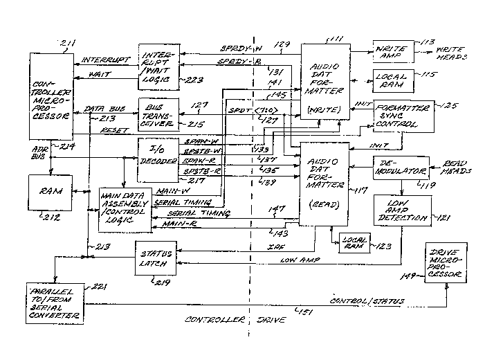
;Referring now to FIG. 3, set forth therein are
components of the drive 11 and controller 13 that are
pertinent to an interface in accordance with the inven-
tion. The drive ll includes a write audio DAT formatter
111 that receives Main Area information and Subarea infor-
mation from the controller, appropriately formats such
information in accordance with the DAT Conference audio
: standard, and provides the formatted information to a
write amplifier 113 which provides recording signals to
the write heads of the drive. A local random access
memory (RAM) is utilized by the write formatter circuit
111 for storage and processing operations.
Generally, the write formatter circuit lll assembles
the data blocks that are to be recorded in the Main Areas
and Subareas of the tape. For example, pursuant to the
ANSI DDS standard, the data blocks for both the Main Areas
and the Subareas are organized substantially identically,
with each block having a Sync area, an ID area, an ID
parity area, and a data area. The contents of the Main
~rea data block data areas is sometimes referred to as
Main data, while the contents of the Subarea data block
data areas i5 sometimes referred to as Sub data. The
information assembled into the data blocks comprises (a)
information provided by the controller and (b) information
generated or calculated by the formatter.
As to the writing of Subarea data blocks, the
controller provides the following information to the write
formatter circuit:
. .
,
~ -:: . :
: .
.. . . . . . ..
: ~ .
' :~ .:
1 (a) the Wl byte for the Sub ID area of each Sub
data block:
(b) the lower order 7 bits of the W2 byte for the
Sub ID of éach Sub data block;
(c) pack data for the data areas of the Sub data
blocks;
(d) pack parity bytes for the pack data items.
As to the writing of Subarea data blocks, the write :~.
: 10 formatter circuit generates or calculates the following
information:
~ '~
(a) the sync bits for 'he Sync area of each Sub
. data block;
(b) the ID parity byte for the Sub ID parity area
of each Sub data block; -::
(c) the Cl ECC error correction parity bytes for
the Sub data block data areas (in accordance
with the DAT Confer nce audio standard);
; 20 (d) the seventh bit of the W2 byte in the Sub ID
area of each Sub data block.
As to the writing of Main Area data blocks, the
; controller provides the following information to the write
formatter:
(a) the Wl byte of the Main ID area of each Main
data block; and
(b) data for the data areas of the Main data blocks
(e.g., user data).
As to writing the Main Area data blocks, the write
formatter generates or calculates the following informa-
tion:
.. 35
.
;.
: ' `'
2~3i~
1 (a) the sync bits for the Sync area of each Main
data block;
(b~ the ID parity byte for the Main ID parity area
o~ each Main data block;
(c) the Cl ECC and C2 ECC error correction parity
bytes for the Main data block data areas (in
accordance with the DAT Conerence audio
standard);
(d) the W2 byte in the Main ID area of each Main
data block.
The drive 11 further includes a read audio DAT
formatter circuit 117 which receives tape data from a
demodulator 119 that is responsive to the outputs of the
read heads of the drive. The read formatter circuit
decomposes the information read from tape in accordance
with the DAT Conference audio standard, so as to provide a
Main Area data output to the controller and to store
Subarea information in predetermined locations in a local
RAM 123 utilized by the read formatter circuit for storage
and processing operations.
A low amplitude detection circuit 121 connected to
` the demodulator 119 provides a low amplitude signal
/LOW-AMP indicative of a playback signal envelope ampli-
~; 25 tude that is below a predetermined level, which indicative
of a bad area on the tape.
Generally, the read formatter circuit disassembles
the Main and Sub data blocks read from tape, checks ID
parity, checks pack parity, checks Cl ECC parity for the
Sub area pack data, checks Cl ECC and C2 ECC parity for
the Main data, and transmits the ECC processed Main data
to the controller, while making other information read
from tape available at predetermined locations in the
local RAM 123, for example.
.
` :
. .
~`' ` ' :
:
'`, ` ': ~ ': `
1 As discussed more fully herein, the write Main data
(designated ADDAT) provided by the controller for the Main
~rea data block data areas is communicated to the write
formatter circuit via a unidirectional serial line, while
the read Main data (designated DADAT) provided by the read
formatter circuit to the controller is communicated via
another unidirectional serial line. Some error detection
information is communicated via dedicated lines, and all
other information transferred between the formatter
circuits and the controller (designated SPDT data) is
communicated via a parallel bus.
In addition to tape data block information, SPDT
data includes control information for the formatter
circuits, such as sample rate, track pitch, and function
(e.g., play, record, high speed). SPDT data also includes
read error processing information as accessed by the
controller from the read formatter circuit.
The parallel SPDT data is transferred between the
write and read formatter circuits 111, 117 and the con-
troller vla a parallel SPDT bus 1~7 that is common to bothformatter circuits. Formatter ready signals SPRDY-W and
SPRDY-R, which indicate that the formatter providing the
signal iq ready to receive or send data on the parallel
SPDT bus 127, are provided by the formatter circuits on
respective lines 129, 131. Address strobe signal~ SPAW-W
and SPAW-R, generated by the controller to transfer
address information to the formatter circuits, are provid-
ed on respective lines 133, 135 to the formatter circuits
111, 117, respectively. Data strobe signals SPSTB-W and
SPSTB-R, generated by the controller to transfer SPDT data
to and from the formatter circuits, are provided on
respective lines 137, 139 connected to the formatter
circuits 111, 117, respectively.
By way of illustrative example, the transfer of SPDT
data can be pursuant to memory maps for the local RAMs of
. . .
. .
.:
.
: - .
~ ~ ~J ~
the formatter circuits, wherein the address locations of
the data identify the nature of the data.
~ain data for and from the data areas of the Main
Area blocks is transfexred between the formatter circuits
111, 117 via respective serial lines 141, 143. In partic-
ular, ADDAT data to be written to tape is serially trans-
ferred from the controller to the write formatter circuit
111 on the serial line 141, while DADAT data read from
tape is transferred from the read formatter circuit 117 to
the controller on thè serial line 143. Depending upon the
tape format specification utilized, the Main Area data
transferred to the write formatter circuit for recording
can be data as to which error correction parity generation
has been performed (e.g., C3 ECC in accordance with the
ANSI DDS standard).
For implementation in accordance with the ANSI DDS
standard, the ADDAT and DADAT data would be logically
organized in groups and Prames that include appropriate
headers in addition to the user data.
Serial timing signals are provided by the respective
formatter circuit~ via respective timing lines 145, 147
which respectively include a plurality of different timing
signals, examples of which will be described in more
; detail urther herein. Generally, such timing signals are
synchxonized to the rotation of the tape head cylinder,
for example by being based on a master signal that con-
trols the rotation of the tape head cylinder, and identify
track boundaries, word boundaries, and bit boundaries.
As to the ADDAT and DADAT serial data, the formatter
circuits 111, 117 generally function as in an audio DAT
application. In particular, the write formatter circuit
lll functions as if it were receiving digital audio data
samples from an analog-to-digital converter; and the read
formatter circuit 117 functions as if it were providing
digital audio data samples to a digital-to-analog
;. ` .. :
.
.., ,, ~ .
.~ , , .
2 ~
1 converter. Stated another way, the ADDAT data to the
write formatter emulates the output of an analog-to-
digital converter ~hat could be utilized in an audio
application, and the DADAT data from the read formatter
circuit emulates the input to a digital-to-analog con-
verter that could be utilized in an audio application.
The read formatter circuit 117 further provides an
interpolation flag signal IPF which indicates that C2 ECC
pari~y check of the data read from tape was unable to
correct detected errors.
A formatter synchronizing control 125 synchronizeq
the operation of the write and read formatter circuits
111, 117 pursuant to a RESET signal provided by the
controller. As discu~sed more fully herein, the syn-
chronizing control 125 synchronizes the opera~ion of the
formatter circuits to allow for read-after-write with a 4
head implementation of the drive.
The drive 11 further includes a drive microprocessor
149 which receives drive commands and provides status
information via drive control/status lines 151. Such
drive commands control the operation of the drive, and the
status information is indicative of the status of the
drive.
The controller 13 include~ a microprocessor 211 for
controlling the operation of the controller, for assembl-
ing the SPDT lnformation transmitted on the parallel bus
127 to the drive, and for processing the SPDT information
accessed ~rom the drive on the parallel bus 127. A RAM
212 is coupled to the microprocessor 211 via a parallel
data bu~ 213 and a parallel addres~ bu~ 214, and is
utilized by the controller microprocessor 211 for storage
and processing operations.
A bus transceiver 215 coupled to the parallel data
bus 213 controls the parallel SPDT bus 127 for transfer of
SPDT information. An in~errupt/wait logic circuit 223 is
.
-
:' ' . ' ' : -
: :
:,
~ ~c3~
1 responsive to the SPRDY signals ancl provides interrupt and
wait signals to the microprocessor 211 for the processing
and transfer of data on the parallel SPDT bus 127, as
discussed in more detail herein.
A main area data assembly/control logic circuit 217
which serializes ADDAT data for transfer to the write
formatter 111 in the drive 11, and further assembles DADAT
data received from the read formatter 117, for example
into groups in accordance with the ANSI D~S standard.
Main Area data and Subarea information as well as
Main data block ID information are transferred concurrent-
ly, although due to processing requirements the Subarea
information being transferred at a given time might not be
associated with the Main Area data being ~ransferred at
that time. Thus, for example, there can be fixed time
relation between (a) the transfer of Main Area data ~via
DADAT or ADDAT) and (b) the transfer or availability of
associated Subarea information and Main data block ID
information (via the SPDT bus). B~ way of illustrative
example, for recording, the Subarea information and Main
data block ID information can be delayed relative to the
associated Main Area data by one or two track intervals;
and for reading, Maln Area data can be delayed relative to
the availability of associated Subarea information by one
or two track intervals. Other read data such as error
counts can also be delayed relative to the availability of
Subarea information. A particular illustrative example of
the timing of the interface signals between the drive 11
and the controller 13 will be discussed further herein.
A status latch 219 is coupled to the data bus 213
and receives the interpolation flag IPF and the low
amplitude signal /LOW-AMP from the drive 11. A parallel/-
serial converter 221 coupled to the data bus 213 is
utilized to transfer control/status information between
. ~
' . ' .:` '. .;, , ~ .~
` . . ~ .:
`
: , , . :-; . .. . :
,
2~5~ ~3~ :
13
1 the controller and the drive on the drive control/status
lines 151.
`~ Drive control information is provided by the con-
troller to control the operation of the drive mechanism,
while drive status information is provided by the drive as
to the status of the drive. Particular examples of drive
control information, drive status information, and for-
mats, and will be discussed further herein.
By way of illustrative example, set forth below is a
specification of signals in accordance with the invention
between the controller and the drive.
DRIVE CONTROL/STATUS
RXD Receive Data From Controller
RXD is used to send commands to the drive. It changes
after the high-to-low transition of TRXCLK. Data transfer
is MSB first. A command transfer can be initiated by the
controller any time /DRDY (discussed below) is asserted.
TXD Transmit Data To Controller
TXD is used to receive drive status. It changes after the
high-to~low transition to RXCLK. Data transfer is MSB
~irst. RXD and TXD data are sent simultaneously and
synchronously.
/TRXCLK ~ransfer Clock From Controller
On or after the low-to-high transition, TXD and RXD are
sampled.
/DRDY Drive Ready To Controller
Asserted when the drive is ready to transfer a byte via
the TXD and RXD lines. Negates after the byte has been
transferred. Asserts again when the drive is ready to
accept the next command.
`~ ' ` ~ ;
~` ~ ' . ; , ' ' : ,
,
.
:~
. , .
: ~ '
3 ~ ~
.
14
'"'
1 /RESET Drive Reset From Controller
Asserted by the controller to initialize the drive to its
starting state. This is a l'hard" reset. It also forces
resynchronization of the write and read formatter cir-
cuits.
.
SPDT DATA TRANSFER TO/FROM WRITE FORMATTER CIRCUIT
,,:
SPDT(7:0) SPDT Data Transfer To/From Controller
Two-way tri-state data bus to both write and read format-
ter circuits. High = 1. Used to transfer ItO. The write
formatter circuit is in the high impedance state when not
enabled by the /SPSTB-W signal (discussed below).
SPRDY-W SPDT Data ReadY To Controller
Indicates that the transfer of SPDT data to the write
formatter circuit possible. In normal write mode, SPRDY-W
is negated when R3CP-W changes, and is asserted beginning
a short interval thereafter, for ex,ample to allow for
processing.
SPRDY-W aan also negated after the end of an /SPSTP-W
pulse (discussed below), for example to allow the write
formatter to access its local RAM if the write formatter
ls relatlvely slower than the controller microprocessor.
/SPAW-W SPDT Address Write From Controller
The low-to-high transition causes the I/O address speci-
fied by SPDT(7:0) to be written into the write formatter
; 30 circuit. This address will be used for the next transfer.
'', '
:'`
~ .
`:`' ' ' '~ ' ', ; ~ ' ' ` .
. ... ~ , ~ , .
... , - : . ~ ~ :
.. . . :
-: . . : : - :
3~'~
1 /SPSTB-W SPDT Data Strobe From Controller
The low-to~high transition causes the data on the SPDT bus
to be transferred to~from the write formatter circuit.
After the SPDT data has been transferred, the write
formatter can increment the selected I/0 address by l,
which would be utilized as the address of the next trans-
fer if no address is specified for such next transfer.
: SPDT DATA TRANSFER TO/FROM READ FORMATTER CIRCUIT
SPDT(7:0~ SPDT Data Transfer To/From_Controller
Two-way tri-state data bus to both write and read format-
ter circuits~ High = 1. Used to transfer I/0. The read
formatter circuit is in the high impedance state when not
enabled by the /SPSTB-R signal (discussed below).
SPRDY-R SPDT Data Ready To Controller
Indicates that the transfer of SPDT data from the read
formatter circuit is possible. In normal read mode,
SPRDY-R i9 negated when R3CP-R changes, and is asserted a
short time thereafter, for example to allow for process-
ing.
SPRDY-R is also negated after the end of an /SPSTB-R pulse
(discussed below), for example to allow the read formatter
to access its local RAM if the read formatter is rela-
tively slower than the controller microprocessor.
' ` ' .
16
l /SPAW-R SPDT Address Write From Controller
;
The low-to-high tran~ition causes the I/O address ~peci-
fied by SPDT(7:0) to be written into the read formatter
circuit. This address will be used for the next /SPSTB-R
transfer. After the SPDT data ha~ been transf~rred, the
read formatter can increment the selected I/O address by
1, which would be utiliz~d as the address of the next
transfer if no address is specified for such next trans-
'` fer.
',,' 10
SERIAL DATA TRANSFER TO WRITE FORMATTER CIRCUIT
~'
R3CP-W Rotation 30 Hz Clock Period To Controller
Hertz cl~ck which is synchronized to the cylinder
ro~ation. The phase is aligned with track write RF
transfers. High = track A (left~, low = track B (right).
The R3CP-W signal is 180 degrees out of phase with the
R3CP-R. R3CP-W changes on the high-to-low transition of
/ADBCK (discussed below). R3CP-W is always present, even
during STOP, UNLOAD, and EJECT modes.
, .
; ADDAT Main Area Write Data From Controller
A continuous serlal bit stream of data to be recorded in
;~ the Main Area of each track. Data i~ sent as 16 bit
i 25 samples synchronized with ADLRCK and /ADBCK. The MSB of
each sample i~ sent first. ADDAT changes on the high-to- -
low transition of /ADBCX.
.
;~ ADLRCK Main Area Write Left/Right Clock To Controller
30 The Main Area write data word sample clock. High = right
channel 16 bit sample, low - left channel 16 bit sample.
Changes polarity on high-to-low transitions of every 16th
/ADBCK. Goes low when R3CP-W goes high.
.
.
, . ~ .
:.. .. ~ . :
: .. ... - . : . : : -
`: : ::: : ' - -
~ ~3~3~ ~
1 /ADBCK Main Area Write Data Bit Clock To Controller
The Main Area write data bit clock. Data on ADDAT is
valid on the low-to-high transition of /ADBCK. R3CP-W,
ADLRCK and ADDAT are changed on the high-to-low transition
of /ADBCK. /ADBCK runs continuously at 32 times ADLRCK.
For a 48 Khz sampling rate, the clock period is 651 nsec.
/NLOAD-W Load Sam~l~ Pulse To Controller
Pulses low for one /ADBCR clock period to indicate the
boundary between successive 16-bit Main Area write data
words. Changes on the low-to-high transition of /ADBCK.
SERIAL DATA TRANSFER TO CONTROLLER
R3CP-R Rotation 30 Hz Clock Period To Controller
30 Hertz clock (during play/record) which is aligned with
track read RF transfers. High = track A (left), low =
track B (right). The R3CP-R signal is 130 degrees out of
phase with the R3CP-W signal. R3CP-R changes on the
high-to-low transition of /DABCK. R3CP-R is always
present, even during STOP, UNLOAD, and EJECT modes.
DADAT Main Area Read Data To Controller
A continuous serial bit stream of data from the recorded
Main Area of each track. Data is received as 16 bit
samples synchronized with DALRCK and DABCK. The MSB of
each sample is sent first. R3CP-R changes on the high-
to-low transition of /DABCK.
DALRCK Main Area Read Left/Right Clock To Controller
The Main Area read data sample clock. High = right
channel 16 bit sample, low = left channel 16 bit sample.
Changes polarity on high-to-low transitions of every 16th
/DABCK.
.
' . ' - : ~
'.~, ' ..
18
1 /DABCK Main Area ~ead Data Bit Clock To Controller
_
The Main Area read data bit clock. Data on DADAT is valid
on the low-to-high transition of /DABCK. R3CP-R, DALRCK
and DADAT are changed on the high-to-low transition of
/DAsCK. /DABCK runs continuously at 32 times DALRCK. For
a 48 Khz sampling rate, the clock period is 651 nsec.
/NLOAD-R Load Sample Pulse To Controller
Pulses low for one /DABCK clock period to indicate the
boundary between successive 16-bit Main Area read data
words. Changes on the low-to-high transition of /DABCK.
IPF Interpolation Fla~ To Controller
Indicates that the current 16 bit PCM sample, as defined
by DALRCK, contains incorrect data (C2 ECC failure). It
is a pulse of nominally 1/2 the length of a DALRCR sample,
centered within the associated DALRCK.
.
/LOW-AMP Low Amplitude To Controller
Asserted whenever the playback signal envelope amplitude
drops below 50~ of the nominal playback envelope ampli-
tude, as determined by a threshold setting.
Referring now to FIG. 4, shown therein is a timing
diagram which sets forth an illustrative example of the
pertinent timing signals discussed above and further
depicts the processing of data being written to tape and
data being read from tape. The timing diagram of FIG. 4
also includes other signals and information that can be
pertinent to a read-after-write procedure which is advan-
tageously implemented in accordance with the invention.
While FIG. 4 depicts the concurrent and phase locked
operation of the write and read formatter circuits for
providing read-after-write, it should be appreciatPd that
write-only and read-only operations can be implemented.
. '.
'` ~.` , : . ' , . . .
.: , . : ,
.
,. . : :
- . ~ ''' '
-:
, , . . : .
:~ . :. -
.
: 19
1 The R3CP-W and R3CP R signals are synchronized with
the rotation of the tape head cylinder, and are phase
locked to each other with a 180 degree phase difference.
A complete cycle of an R3CP signal represents one revolu-
tion of the tape head cylinder.
The ADDAT serial data to be recorded and the DADAT
serial data from tape are transferred to and from the
- drive concurrently, with the frame, track, word and bit
boundaries being identified by the transitions of the R3CP
signals and the other timing signals discussed above. In
particular, during each of the MAIN DATA OUT intervals
that are defined by the positive going transitions of the
R3CP-W signal, Main Area data for a frame is transferred
~o the drive. Similarly, during each of the MAIN DATA OUT
intervals defined by the positive going transitions of the
R3CP-R signal, Main Area data for a frame is transferred
to the controller.
While the frame boundaries are indicated by MAIN
DATA OUT and MAIN DATA IN as coinciding with the positive
transitions of the R3CP-W and R3CP-R signals, the phasing
of the frame boundaries can be different, depending on
implementation and processing requirements. The important
consideration is that frame boundaries be defined by
intervals that each equal one cycle of the R3CP signals.
For example, the frame boundaries of MAIN DATA OUT can
; lead the positive transitions of R3CP-W by a predetermined
number of bit intervals, and the frame boundaries of MAIN
DATA IN can lag the positive transitions of R3CP-R by a
predetermined number of bit intervals.
The interpolation flag signal IPF is also provided
during the MAIN DATA IN intervals during each word, for
example in the middle of the word interval with which the
particular IPF signal is associated, as discussed above in
` the illustrative examples of signal specifications.
: - , . . .
:: . : : . . ::
.: , :.
: - - . : ~ :
~3:~3i~
1 SPDT data, including tape Subarea information and
Main data block ID information, can be transferred on the
SPDT parallel bus during the intervals identified by SUB
DATA orJT and SUB DATA IN, wherein OUT refers to transfers
the write formatter circuit 111, and IN refers to trans-
fers between the read formatter circuit 117 and the
controller. As discussed above, the SPDT data can include
control information for the formatter circuits, which
would require transfer to the formatter circuits. The
reference to SUB DATA in the timing diagram of FIG. 4 is
to indicate that Subarea information is to be provided or
is available via the SPDT parallel bus during the SUB DATA
intervals identified in the timing diagram, with the
direction of transfer being indicated by OUT and IN.
The SUB DATA OUT intervals are defined by the
logical AND of the R3CP-W signal and the SPRDY-W signal
that is not shown but is essentially the same as the
SPRDY-R signal, and the SUB DATA IN intervals are defined
by the high states of the SPRDY-R signal. The SUB DATA
OUT intervals are defined in this manner to provide a
~ingle SU~ DATA OVT interval for each cycle of the R3CP-W
signal, which is appropriate for a tape format in accor-
dance with the ANSI DDS standard that requires that the
subarea~ in both tracks of a frame be identical. However,
it should appreciated that two SUB DATA OUT intervals can
be provided for each R3CP-W cycle if the two tracks of a
frame are to include different Subarea information.
It should be noted that the SUB DATA OUT and SUB
DATA IN references indicate when Subarea information and
any Main Area informa~ion communicated via the SPDT bus
are transferred from the controller (OU~) and to the
controller (IN).
The direction of transfer of SPDT data on the SPDT
parallel bus 127 and the formatter circuit being accessed
at any given time are controlled by the microprocessor and
, - , . , , . .. , .. ,:
, ~ . " , ~ . ...... :
., , , ~ - : :
:. .: , . . . .
.: ~ ,-. . , : , , .. -, .
2~-3:1335~
21
1 the I/O decoder 217. By way of illustrative example, the
locations in memory maps associated with each of the
formatter circuits can be designated as write-only or
read-only, and thus the formatter circuit and address
being accessed can implicitly define direction.
More particularly as to the function of the SPRDY
signals, the interrupt/wait logic circuit 223 can provide
an interrupt pursuant to a SPRDY signal becoming active
after a transition of the associated R3CP signal to
indicate that data can be transferred on the parallel SPDT
bus 127. A wait signal can be provided if the formatter
circuits are slower than the controller microprocessor
211, for example pursuant to a SPRDY signal becoming
inactive prior to the next transition of the associated
R3CP signal. Accordingly, although not shown in FIG. 4,
the SPRD~ signals could have relatively short negative
pulses between the negative pulses at the transitions of
the associated R3CP signals. The interrupt/wait logic
circuit would be configured to provide the appropriate
interrupt or wait signal, for example, as function of the
transitions of the R3CP ~ignals.
RFOUT identifies the intervals during which one of
the write heads i8 in contact with the tape, and RFIN
identifies the intervals during which one of the read
heads is in contact with the tape. In terms of relation
to the R3CP signals, RFOUT intervals start with each
transition of the R3CP-W signal and continue for 90
degrees of thè R3CP-W cycle, while RFIN intervals start 90
degrees after each transition of the R3CP-R signal.
FIG. 4 further illustrates the timing sequence for
writing and reading of a given frame. The Main Area data
for the frame N is transferred to the write formatter
during the first cycle of the R3CP-W signal associated
` with the frame N. During the second R3CP-W cycle associ-
;, 35 ated with the frame N, Subarea information and Main data
-
22
1 block ID information for the frame N are transferred via
the ~PDT parallel bus~ The first track (A) of the frame N
is written to tape during first 90 degrees of the third
R3CP-W cycle associated with the frame N, and the second
track (B) of the frame N is written to tape during the
third 90 degrees of the third R3CP-W frame associated with
; the frame N. Thus, in terms of transferring frame infor-
mation to the write formatter circuit and writing the
frame to tape, three cycles of the R3CP-W signal are
` 10utilized, with the frame information being processed in
pipeline fashion.
As to reading, the first track (A) of the written
frame N is read from tape during the fourth or last 90
degrees of the third R3CP-W associated with the frame N.
The second track (B) is read during the second 90 degrees
of the fourth cycle of the R3CP-W signal associated with
the frame N. The first track Subarea information is
available a short time after the start of the fourth
R3CP-W cycle associated with the frame N, to allow for
processing after reading, and the second track Subarea
information i5 available a short time after the 180 degree
transition o the ourth R3CP-W cycle associated with the
frame N, also to allow for processing.
In the fore~oing read-after-write procedure, a track
is read after another adjacent track has been written, in
other words by the read head positioned 270 degrees from
` the write head that wrote such track, in the direction of
rotation. In this manner, a recorded track is read in its
final form with recorded tracks on either side.
; 30 The Main Area data as read for the frame N is
transferred to the controller during the last 180 degrees
of the fifth cycle of the R3CP-W signal associated with
; the frame N and the first 180 degrees of the sixth cycle
of the R3CP-W signal associated with the frame N.
... ..
~ ~ ~ a
23
1In terms of the R3CP-R signa:L, with the first cycle
of the R3CP-R signal associated with the frame N being
that cycle during which the first track for the frame N is
read from tape as identified by RFIN, the Subarea informa-
tion for the first and second tracks are available during
the last half of the first R3CP-R cycle associated with
the frame, and during the first half of the second R3CP-R
cycle associated with the frame. Main Area data read for
the frame N is available during the third cycle of the
R3CP-R signal associated with the frame N. In other
words, reading a frame from tape and transferring the
frame information to the controller takes place over three
cycles of the R3CP-R signal, with the frame information
being processed in pipeline fashion.
15Further as to reading the frame N, FIG. 4 illus-
trates the availability of certain error data that can be
utilized for determining whether re-write is necessary.
A Main Area ID parity error count IDPCNT, a subcode
odd parity error count SOPCNT, a subcode even parity error
count SEPCNT, and the LOW AMP signal are available for the
first track during the second half of the first R3CP-R
; cycle, and are available or the second track during the
first half of the second R3CP-R cycle. The "odd" and
"even" terms refer to odd and even numbered blocks. The
~oregoing counts are accessed via the SPDT parallel bus,
while the LOW AMP signal is provided on a separate line.
`` The Cl ECC processing error count for the Subareas
of the ~ir~t track is available during the first half of
the second R3CP-R cycle, while the Cl ECC processing error
count for the Subareas of the second track is available
during the second half of the second R3CP-R cycle. The Cl
;` ECC processing error count for the Main Area of the first
track is available for the first track during the second
half of the second R3CP-R cycle, while the Cl ECC process-
ing error count for the Main Area of the second track is
.,
... .
: , : . : ,
,: .
- . :.
. . . .. ' '.: ~ : ' .
24
1 available during the first half of the third R3CP-R cycle.
- The foregoing Cl error counts are accessed by the con-
troller via the SPDT parallel bus.
The controller generates a checksum for the Main
`/ 5 Area informa*ion, which is checked against checksurn
information in the Subarea information for the frame N
during the fourth cycle of R3CP-R.
In terms of re-write after reading, such re-write
can commence as early as the fifth cycle of the R3CP-W
signal associated with the frame (i.e., four frames
later), or as late as the seventh cycle of the R3CP-W
signal (i~e., six frames later), depending upon the nature
of the error detected that calls for a re-write.
Further as to the communication of the drive control
and status information on the control/status lines 151,
; control information transmitted to the drive via the RXD
signal discussed above can include two categories, drive
; modes and drive commands, examples of which are set forth
further herein. Drive modes generally are directed to
drive control operations such as mechanism mode changes
; that require a relatively longer time to complete, and as
to which the controller obtains mode status information to
detect that the requested mode is active. Drive commands
generally are directed to drive operations that can be
completed relatively quickly.
Drive modes and commands can include the following:
i,
DRIVE MODES
,
cassette load
cassette eject
~` tape unload, cylinder stop
~; cylinder run, tape load
skip Device Area of tape
soft stop motion
hard stop motion
i,
. .
. : , . - . :
., ~ ~ ,.............. :
., . ,. .. . - , --:
~3~
1 pause
forward Xl
forward X3
forward X5
S forward X7
forward Xll
forward X12.5
- forward X15
forward X25
forward X50
forward X75
forward X100
forward X150
forward X200
forward X250
forward X300
forward X400
cylinder stop
cylinder run
reverse Xl
reverse X3
reverse X5
reverse X7
reverse X11
` 25 reverse X12.5
reverse X15
reverse X25
reverse X50
reverse X75
reverse X100
reverse X150
reverse X200
.~ reverse X250
rev~rse X300
reverse X400
.,
.
.` ' ~ . ; - ' ' '' . ' ~ :
., .~ ,. . . , :,
~: . . .. . ` .
.
' ., , ~ : : ~ - : ~ : - : .
.. : . . . .
.. : . . ~ .
.:
2 ~
26
DRIVE COMMANDS
. _ _
get drive mode
clear eject request bit
set constant speed servo (record)
set ATF servo (play)
cassette status LED off
cassette status LED on
drive LED off
drive LED on
allow media removal
prevent media removal
get hole status
get cassette status
get error status
get drive status
set 13.6 um track width (read/write)
set 20.4 um tracX width (read only)
drive reset, clear errors
; 20 An illustrative example of the format of an 8-bitcontrol information byte i5 set forth in FIG. 5, wherein
the type of the control information (drive mode or drive
command) is identified by bit 6 or 7 being set to 1. If
both bits 6 and 7 are set to 0, the control information is
a no-operation.
Status information provided by the drive via the TXD
signal discussed above can include information as to
status of the drive modes requested by the controller, and
also the particular status information requested via drive
commands. FIG. 6 sets forth an illustrative example of an
8-bit status information byte that can be utilized to
communicate status information. If bit 7 is 1 and bit 5
is 0, the drive is currently changing to the drive mode
identified in bits (5:0). If bit 7 is 0 and bit 6 is 1,
the drive is in the mode identified by bits (5:0). If
: ' ,
': '
2 ~
27
`
1 both bits 7 and 6 are 1, the drive mode or drive command
last sent by the controller has been rejected, and bits
' (5:0) identify the rejected mode or command.
If both bits 7 and 6 are 0, the status format is as
shown in FIG. 7. In particular, bit 5 comprises an Eject
Requested bit, while bits (4:0) identify a drive status,
cassette status, hole status, or error status codes. The
particular status byte can be presented in response to a
command, as a result of an error condition, or as a result
of operator actuation of a drive Eject button while the
drive is operating puxsuant ~o a "prevent media removal"
command.
In terms of control/status communications for an
implementation wherein control information and s~atus
information are communicated only simultaneously pursuant
; to control by the controller (i.e., full duplex communica-
tion wherein drive control is slaved to the controller), a
drive status or error code can be returned in response to
a drive mode code, with the error code having higher
pxiority. If a drive command is communicated, then the
appropriate status code must be returned.
The cassette status, drive status, and error status
information can include the following:
CASS~TTE STATUS
no cassette
cassette loading
cassette loaded, length unknown
cassette loaded, length = 120 min.
cassette loaded, length = 90 min.
cassette loaded. length = 60 min.
cassette loaded, length = 45 min.
DRIVE STATUS
__
no status availabla
,
,
.: , . . .
. : ~
- - . . . .
.. .
2 ~3 ~ J~
28
1 Beginning of Tape tBOT) lead~r detect
: End of Tape ~EOT) leader detect
adjust threshold complete
S ERROR STATUS
no error
cassette loading error
cassette eject arror
, capstan error
cylinder error
reel error or tape jam
. mechanism error
tape cut . -
adjust threshold error :
no cassette ~ :
dew detected, ~ape, unloaded - ~ :
. :
As to tape cassette hole status, FIG. 8 sets for a
particular example of the format for the code bits of the
status ~yte of FIG. 7. Bit 4 is set to indicate that the
tape is write-protected; and bit 3 is set to indicate that
the tape i9 pre-recorded. Bits (2:0) indicate tape type,
whlch can include the following:
TAPE TYPE
: 25 metal power or equlvalent, 13 um thickness
metal power or equivalent, thin
wide track, 13 um thickness
cleaning cassette
' wide track, thin . :
As to cassette ejection, whether or not cassette
ejection is permitted can be controlled by the controller,
for example to prevent removal of a cassette while record-
ing. After the "allow media removal" command has been
sent to the drive, the drive will eject the cassette
~ . . , . ~
- . ' ~ ' -
: - ~ -. , - - .: .. ' :
2 ~
29
1 immediately after the Eject button is pushed by an opera-
tor. This can also be the default mode after reset. If
the controller sends a command after the cassette has been
ejected, an error status indicating no cassette will be
rPturned by the drive.
After the "prevent media removal" command has been
sent to the drive, the drive will set the Eject Requested
status bit when the Eject button is actuated, and the
cassette will not be ejected. This status remains until
the controller issues a "cassette eject" command, a "clear
Eject Reques~" command, or an "allow media removal"
command, at which time the cassette will be ejected.
Referring now to FIG. 9, set forth therein by wa~ of
; illustrative example is a flow diagram of a process that
can be implemented with the foregoing drive/controller
interface for reading a computer storage DAT tape. At 311
the controller provides a drive mode to the drive via the
control/status lines 151 to set the drive mechanism mode
to forward at the normal speed of Xl. At 312 the control-
ler requests the drive mode status, and at 313 a deter-
mination is made as to whether the requested mode is
active. If no, control transfers to 312. This is to
allow time for the mode change to be completed.
If the determination at 313 is yes, the requested
mode o forward Xl is active, a set ATF servo command is
provided by the controller at 315. At 317 the read
formatter is set to play, for example, pursuant to format-
ter control data provided by the controller on the SPDT
parallel bus.
At 319 the Subarea and Main Area information read
from tape are processed as discussed above. As the tape
is being read, at 321 the controller periodically requests
information as to the drive status, via the control/status
; lines. At 323 a determination is made as to whether the
~ 35 drive status provided in response to a request at 321
`;''
. .
.. ~' ;'., ~.;. . ' : ' ' ' .'
.. . .. . .
: . .
v
1 indicates the end of tape or an error. If no, a determin-
` ation is made at 325 as to whether xeading of the selected
information, certain specified groups, for example, has
been completed. If no, control transfers to 319 for
processing Subarea and Main Area information.
If the determina~ion at 323 is yes, or if the
determination at 325 is yes, the controller requests the
drive to engage the stop mode at 327. At 328 the control-
ler requests the drive mode status, and at 329 a deter-
mination is made as to whether th~ requested mode i5active. If no, control transfers to 328. When the stop
mode is active, the drive has stopped and the read process
is completed.
Other processes for tape operation~ will be readily
apparent to those skilled in the art.
The foregoing has been a disclosure of an interface
for use with a computer DAT drive that includes components
developed ~or audio DAT applications, and which advanta-
geously provides for recognition of frame boundaries,
phase-locked operation of the drive read and write format-
ter circuits, read-after-write capability, full format
capability as to Sub and Main Areas, and precise tape
drive mechanism control.
Although the foregoing has been a description and
illustration of specific embodiments of the invention,
` various modifications and changes thereto can be made by
; ~ persons skilled in the art without departing from the
scope and spirit of the invention as defined by the
following claims.
.'; .
:
.,
~ . . .
., : . . .
,. ~ . .
.' . ' ~.