Note: Descriptions are shown in the official language in which they were submitted.
- 20316~2
TITLE OF THE lNv~NllON
Method of Manufacturing Oxide Superconducting Wire
BACKGROUND OF THE lNv~NllON
Field of the Invention
The present invention relates to a method of
manufacturing an oxide superconducting wire, and more
particularly, it relates to an improvement for increasing
critical current density and elongation workability of an
oxide superconducting wire which is prepared from powder
raw material for a superconductor.
Description of the Background Art
A specific material exhibits diamagnetism under a
superconducting phenomenon such that no voltage potential
difference is developed although a finite stationary
current flows in its interior.
This superconducting phenomenon is applied to an
extremely wide range of fields such as that of electric
power including MHD power generation, power transmission
and power storage and that of transportation including a
magnetic levitation train and an electromagnetically
propelled ship. Further, a supersensitive sensor for a
magnetic field, a high frequency, radiation rays or the
like using the superconducting phenomenon is applied to
the fields of measurement including nuclear magnetic
resonance (NMR), ~-meson remedy and a high energy physical
- 1 - ~
2031692
experimental apparatus, while the superconducting
phenomenon is also expected in the field of electronics,
which is represented by the Josephson device, as a
technique which can not only reduce power consumption but
implement an element of extremely high-speed operation.
Superconductivity was until recently only observed
under a very low temperature. Even Nb3Ge, which has been
referred to as that having the highest critical
temperature Tc of superconductivity among conventional
superconducting materials, has an extremely low critical
temperature of 23.2 K, and this value has been regarded as
the limit critical temperature of superconductivity for a
long period of time.
Therefore, a superconducting material has been
generally cooled to a temperature below the aforementioned
critical temperature with liquid helium which boils at 4.2
K, in order to implement a superconducting phenomenon.
However, such employment of liquid helium leads to
technical and economic burdens due to cooling equipment
including liquefaction equipment, to hinder implementation
of the superconducting technique.
On the other hand, it has been recently reported that
a composite oxide sintered body can exhibit
superconductivity at a high critical temperature, and
development of the superconducting technique is abruptly
2031692
being prompted with a superconductor whose critical
temperature is not very low. It has been reported and
recognized that a YBaCuO material superconducts at 90 K,
and BiSrCaCuO and BiPbSrCaCuO materials superconduct at
110 K, respectively.
In order to manufacture a wire by the aforementioned
composite oxide sintered body, i.e., an oxide
superconductor, the following method has been tried, for
example: First, powder is prepared by repeating a step of
heating an oxide superconductor or raw material therefor
and thereafter pulverizing the same a plurality of times.
This powder is then covered with a sheath of a metal or an
alloy which is unreactive and nonreductional with respect
to the powder at a temperature of not more than 950C.
The sheath thus filled up with the powder is so deformed
that its diameter is reduced. An elongated wire is
obtained in this stage. Then, this wire is heat treated.
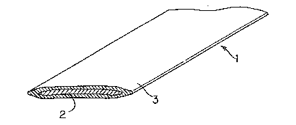
Fig. 1 shows a superconducting wire 1 obtained in the
aforementioned manner. This superconducting wire 1
comprises a superconducting part 2 of an oxide
superconductor, and a sheath 3 formed to enclose the
superconducting part 2. The sheath 3 is made of silver or
a silver alloy, for example.
In the aforementioned method of manufacturing an
oxide superconducting wire, however, the powder of the
- 2031692
oxide superconductor or raw material therefor may generate
gas during heat treatment of the wire obtained by
deformation processing, such that a void 4 is defined in
the superconducting part 2 to inflate the sheath 3, as
shown in Fig. 2. If such inflation is caused in the
superconducting wire 1, its critical current density Jc is
reduced. In order to increase critical current density of
the superconducting wire 1, therefore, it is necessary to
prevent such inflation in the superconducting part 2.
In general, the aforementioned inflation in the
superconducting part 2 is not uniformly caused
longitudinally along the superconducting wire 1, but
ununiformly distributed in a plurality of portions along
the longitudinal direction. If such inflation takes
place, therefore, it is difficult to obtain a
superconducting wire which has small distribution of
critical current density Jc along the longitll~;n~l
direction.
SUMMARY OF THE lNv~NllON
Accordingly, an object of the present invention is to
provide a method of manufacturing an oxide superconducting
wire, which can solve the problem of inflation of a
superconducting part, thereby providing high critical
current density.
Another object of the present invention is to provide
2031692
a method of manufacturing an oxide superconducting wire
with smaller dispersion of critical current density along
the longitudinal direction.
The inventive method of manufacturing an oxide
S superconducting wire comprises:
(1) a step of preparing powder by repeating heat
treatment and pulverization of an oxide superconductor or
raw material therefor a plurality of times:
(2) a step of covering the powder with a sheath of a
metal or an alloy which is unreactive and nonreductional
with respect to the powder at a temperature of not more
than 950C;
(3) a step of deforming the sheath which is filled up
with the powder; and
(4) a step of heat treating a wire obtained by the
deforming step.
In order to solve the aforementioned technical
problem, the present invention further comprises a step of
re-heating the powder between the step (1) of preparing
powder and the step (2) of covering the powder with a
sheath.
After the aforementioned re-heating step, a process
of softly pulverizing the powder to an extent allowing no
adsorption of gas nor fine particles may be introduced
within the scope of the present invention.
2031692
In another aspect of the present invention, the
inventive method comprises a process of heating the powder
under a decompressed atmosphere of not more than 850C in
at least part of the heat treatment included in the step
(1) of preparing powder and/or part of the step (4) of
heat treating the wire, in order to solve the
aforementioned problem.
More preferably, the inventive method may further
include a step of heating the powder under a decompressed
atmosphere of not more than 850C between the step (1) of
preparing powder and the step (2) of covering the powder
with a sheath.
After the aforementioned heating step is carried out
in advance of the step (2), a process of softly
pulverizing the powder to an extent allowing no adsorption
of gas nor fine particles may be introduced within the
scope of the present invention.
The sheath is preferably formed of silver or a silver
alloy.
The oxide superconductor is preferably prepared from
BiPbSrCaCuO, BiSrCaCuO, Tlsacacuo~ TlBiSrCaCuO,
TlPbBaCaCuO or TlPbSrCaCuO oxide superconductor material.
According to the present invention, fine particles or
gas adsorbed by the powder can be desorbed by heating the
powder at least once preferably under decompression in a
-- 6
2031692
stage before final sintering of the powder. The adsorbed
fine particles or gas can be further withdrawn by heating
the powder under decompression at least once before the
same is covered with the sheath, then covering the powder
with the sheath, deforming the sheath and again heating
the same under decompression, for example. Thus, it is
possible to prevent gas generation from the powder during
heat treatment for growing superconductive particles,
thereby preventing the superconducting wire from inflation
etc. caused by such gas generation.
Thus, according to the present invention, the
superconducting wire can be prevented from inflation so
that no cracking etc. is caused in a superconducting part
which is provided in the superconducting wire. Thus, a
cause for reduction of critical current density can be
eliminated, whereby it is possible to obtain an oxide
superconducting wire which can provide high critical
current density, as well as to extremely reduce dispersion
of critical current density along the longitudinal
direction of the superconducting wire.
Thus, the oxide superconducting wire according to the
present invention is particularly effectively applicable
to a magnet coil or a superconducting cable, which is
prepared from an elongated wire.
These and other objects, features, aspects and
2031692
advantages of the present invention will become more
apparent from the following detailed description of the
present invention when taken in conjunction with the
accompanying drawings.
BRIEF DESCRIPTION OF THE DRAWINGS
Fig. 1 is a perspective view showing a part of an
oxide superconducting wire 1 to be obtained according to
the present invention; and
Fig. 2 is a perspective view showing a part of an
undesirably inflated oxide superconducting wire 1.
DESCRIPTION OF THE PREFERRED ENBODINENTS
Example 1
Powder was prepared by mixing Bi2O3, PbO, SrCO3, CaCO3
and CuO so that Bi, Pb, Sr, Ca and Cu were in composition
ratios of 1.8:0.4:2:2.2:3.
This powder was heat treated at 800C for eight
hours, and then the heat-treated substance was pulverized
into powder in an automatic mortar for two hours.
Thereafter the pulverized substance was heat treated at
860C for eight hours, and then the heat-treated substance
was again pulverized into powder similarly to the above.
This powder was divided into halves, and treated as
follows:
The first half was directly filled up in a silver
pipe of 6 mm in outer diameter and 4 mm in inner diameter
2031692
and then subjected to wire drawing and rolling, to prepare
a tape-type wire of 0.2 mm in thickness (wire 1).
The second half was again heated at 800C for 15
minutes, and then filled up in a silver pipe which was
similar to the above, and worked into a wire by a similar
technique (wire 2).
The as-formed wires 1 and 2 were heat treated in the
atmospheric air at 845C for 50 hours. As the result, the
wire 1 was inflated as shown in Fig. 2, while no inflation
was caused in the wire 2, as shown in Fig. 1. The
inflated wire 1 substantially passed no current, while the
wire 2 exhibited critical current density of 12500 A/cm2
in liquid nitrogen (77.3 K). Table 1 shows states of
distribution of critical current density in ranges of 5 m
along longitudinal directions of the wires 1 and 2. As
understood from Table 1, dispersion of critical current
density of the wire 2 was within about 20 %.
Table 1
Wire 1 Wire 2
1 [m]100 A/cm2 11500 A/cm2
Longitudinal 2 50 " 12500 "
Distribution 3 0 " 11000 "
Along Wires 4 120 " 12100 "
" 10800 "
Dispersion 100 % 20 %
- 2031692
Example 2
The wires 1 and 2 obtained in Example 1 were further
rolled to be 0.15 m~ in thickness, and then heat treated
at 840C. Table 2 shows states of distribution of
critical current density of the wires 1 and 2. As
understood from Table 2, the wire 2 exhibited superior
results with respect to dispersion of critical current
density.
Table 2
Wire 1 Wire 2
1 tm]5000 A/cm2 15000 A/cm2
Longitudinal 2 1000 " 14500 "
Distribution 3 0 " 16000 "
Along Wires 4 1500 " 15400 "
2300 " 15100 "
Example 3
Powder was prepared by m;xing Bi2O3, PbO, SrCO3, CaCO3
and CuO so that Bi, Pb, Sr, Ca and Cu were in composition
ratios of 1.8:0.4:2:2.2:3.
This powder was heat treated at 800C for eight
hours, and the heat-treated substance was pulverized into
powder in an automatic mortar for two hours. Thereafter
the pulverized substance was heat treated at 860C for
-- 10 --
2031692
eight hours, and then the heat-treated substance was again
pulverized into powder similarly to the above. This
powder was divided into halves, and treated as follows:
The first half was filled up in a silver pipe of 6 mm
in outer diameter and 4 mm in inner diameter for serving
as a sheath, and then subjected to wire drawing and
rolling, to prepare a tape-type wire of 0.2 mm in
thickness (wire 3).
The second half was again heated under decompression
of 20 Torr at 700C for 30 minutes, and thereafter filled
up in a silver pipe which was similar to the above, and
worked into a wire by a similar technique (wire 4).
The as-formed wires 3 and 4 were heat treated in the
atmospheric air at 845C for 50 hours. As the result, the
wire 3 was inflated as shown in Fig. 2, while no inflation
was caused in the wire 4, as shown in Fig. 1. The
inflated wire 3 substantially passed no current, while the
wire 4 exhibited critical current density of 12500 A/cm2
in li~uid nitrogen (77.3 K). Table 3 shows states of
distribution of critical current density in ranges of 5 m
along longitudinal directions of the wires 3 and 4. As
understood from Table 3, dispersion of critical current
density was within about 20 % in the wire 4.
2031692
Table 3
Wire 3 Wire 4
1 [m] 100 A/cm2 12000 A/cm2
Longitudinal 2 50 " 12300 "
Distribution 3 0 " 15000 "
Along Wires 4 120 " 13200 "
" 14000 "
Dispersion 100 % 20 %
Example 4
The wires 3 and 4 obtained in Example 3 were further
rolled to be 0.15 mm in thickness, and then heat treated
at 840C. Table 4 shows states of distribution of
critical current density of the wires 3 and 4. As
understood from Table 4, the wire 4 exhibited superior
results as to dispersion of critical current density.
Table 4
Wire 3 Wire 4
1 [m] 5000 A/cm2 20000 A/cm2
Longitudinal 2 1000 " 18500 "
Distribution 3 0 " 21200 "
Along Wires 4 1500 " 19400 "
2300 " 18700 "
- 12 -
2031632
Example 5
The wires 3 and 4 obtained in Example 3 by wire
drawing and rolling were heated under decompression of 20
Torr at 700C for 30 minutes, thereafter sintered in the
atmospheric air at 845C for 50 hours, and subjected to
the working and heat treatment mentioned in relation to
Example 4. As the result, no inflation was caused in the
wire 3, which had been inflated in Example 3. As shown in
Table 5, the wire 3 exhibited higher critical density as
compared with Examples 3 and 4, with smaller dispersion.
The wire 4 also exhibited higher critical current density
as compared with Examples 3 and 4, with smaller
dispersion.
Table 5
Wire 3 Wire 4
1 Lm~.1100 A~cm2 28000 A/cm2
Longitudinal 2 8000 " 26000 "
Distribution 3 5600 " 29000 "
Along Wires 4 7000 " 27000 "
10300 " 29000 "
Although the present invention has been described and
illustrated in detail, it is clearly understood that the
same is by way of illustration and example only and is not
- 13 -
2031~92
to be taken by way of limitation, the scope of the present
invention being limited only by the terms of the appended
claims.
- 14 -