Note: Descriptions are shown in the official language in which they were submitted.
2031712
TITLE OF THE INVENTION
DEVICE FOR SUPPRESSING VOLTAOE FLUCTUATION AND
HIGHER HARMONICS
BACKGROUND OF THE INVENTION
Field of the Invention
This invention relates to a device for suppressing
voltage fluctuation and higher harmonics of the power
system that are generated due to power fluctuation of the
load with a large amount of power fluctuation and higher
harmonic current.
Description of the Related Art
Conventionally, when suppressing voltage fluctuations
of a power system generated from a load with irregular
fluctuations of reactive power and large capacity, such as
an arc furnace, it has been the practice to control the
reactive power of a voltage fluctuation suppression device,
which was provided in parallel with the load in order to
compensate for these fluctuations of reactive power, by
detecting the reactive power consumed by the load.
Fig. 4 shows a circuit layout of a conventional
voltage fluctuation suppression device, which is disclosed,
for example, in U.S. Patent No. 4,752,726 (June 21, 1988).
In Fig. 4, to avoid complicating the drawing, the
three-phase system is shown as a single line connection
diagram. In Fig. 4, power is fed to a load 1 from a power
source 2 through a transmission line 3 (asssumed to be of
impedance jXs) and a receiving transformer 4 (assumed to be
2Q~1712
of impedance jXt). A voltage fluctuation suppression
device constituted by a self-commutated converter 10 is
provided in parallel with the load 1. This includes a
control circuit 20 wherein the reactive power is calculated
from the current and voltage detected by a current
transformer 5 and a voltage detection transformer 6, and a
current to compensate for the reactive power is supplied.
As shown in Fig. 5, the self-commutated conveter 10
includes ac reactors 12, gate turn-off thyristors (GTO) 13,
diodes 14, and a dc capacitor 15. The current of the load
1 detected by the current transformer 5 is the line current
of the three-phase circuit and is converted to the
two-phase ac by a three-phase/two-phase conversion circuit
21. This process can be represented by the following
equation, where iR, is and iT are the respective line
currents of the three-phase ac, and id and iq are the
currents of the two-phase ac.
id~ 1/2 1/2 ~iRl ... (1)
0 ~7~ iTJ
In the same way, the circuit voltages VR, vs, vT are
detected by the voltage detection transformer 6, and
converted to the two-phase ac by a three-phase/two-phase
conversion circuit 22. The expression representing this
conversion is the same as equation (1), substituting v for
i.
-1/2 -1/2 ]~vR~ ... (2)
vq- 0 ~7~ ~ VT
2~317:12
The voltage signals vd and vq obtained by this
two-phase conversion are converted by a synchronization
detection circuit 24 into synchronized voltage signals Vd*~
vq* synchronized with the fundamental component. A
reactive power detection circuit 23 detects the so-called
instantaneous real power and instantaneous imaginary power,
as defined in Article No. 58-B60, P. 41 to 48 of Denki
Gakkai-Shi Ronbun (The Journal of the Electrical
Association of Japan) "Generalized Theory of Instantaneous
Reactive Power and its Application". These are found by
calculation by the following expression:
[P~ = [iid iql lVd*l ... (3)
where p is the instantaneous real power and q is the
instantaneous imaginary power. In the two-phase ac, Vd*
and vq* are orthogonal components of magnitude 1 pu, and vd
approximately equals Vd* and vq approximately equals vq*.
p is therefore the instantaneous active power supplied from
the power source 2 to the load 1, and q is the instantaneous
reactive power circulating between the two phases.
Also in the power system, the magnitude of the voltage
fluctuations due to reactive power is dominant, and the
fluctuations due to active power can be neglected. The
self-commutated converter 10 need therefore only compensate
q. The compensation amounts q* can therefore be obtained
by an inverter circuit 25 by inverting q* the sign of q, as
q* = _q ... (4)
2Q~1712
An instantaneous current calculation circuit 26
calculates the respective line current command values iCR*,
iCS* and iCT* to make the self-commutated converter 10 act
as a curernt source. These are found by inverse conversion
of expression (3) and expression (1). Taking the command
values in the two-phase ac as icd* and icq*, these are
given by:
[iicd*] = [vd* -vqd*~ [q*~
i *~ -1/2 ~ 1 ~ cd I ... (6)
iCT*' -1/2 -~7~ cq
Since, for the reasons discussed above, p* = O, we
have:
i *~ ~ 1 0 ~ rv * q*~
iCR*~ 7~ -1/2 ~ I , q ' ... (7)
-iCT*J ~-1/2 -~7~J ~v * q*i
An calculation circuit 27 calculates the differences
between the respective currents iCR, iCS and iCT of the
self-commutated converter 10 detected by the current
transformer 11 and the command values found from the above
equation. An error amplifier 28 uses these differences to
perform constant-current control, tracking the command
values of the converter 10. The outputs of the error
amplifier 28 are input to an gate circuit 29, generating
on/off pulses for PWM control of the converter 10, these
pulses being applied to the gates of GTOs 13 shown in
2~171 2
.
Fig. 5. Since this self-commutated converter 10 is of the
voltage type, the dc capacitor 15 is needed to make the dc
voltage constant. An ac reactor 12 performs the action of
smoothing the pulse-width modulated voltage and converting
it to a current.
While voltage fluctuations are controlled as above, a
higher harmonic filter 7 consisting of a reactor and a
capacitor is provided in order to suppress higher harmonics
generated by the load 1. Such a filter is a so-called
single harmonic tuning type passive filter, so a group of
higher harmonic filters are constituted by providing one or
more higher harmonic filters for the higher harmonics of
each order.
Thus, in a conventional device for suppressing voltage
fluctuation and higher harmonics, higher harmonic filters
were used as higher harmonic suppression means. However,
such a higher harmonic filter cannot suppress all higher
harmonics, it cannot suppress higher harmonics corresponding
to the antiresonance frequency determined by the constant
of the higher harmonic filter and the reactance Xs of
transmission line. In particular in the case of an arc
furnace, when the higher harmonics vary steeply and
irregularly, the higher harmonics cannot be suppressed by
the higher harmonic filter, and may in fact be increased.
The voltage fluctuation and higher harmonic
suppression device as shown in Fig. 4 wherein the higher
harmonic filter 7 and the self-commutated converter 10 are
20~17'~2
connected in parallel to the load 1 has in principle the
capability of suppressing higher harmonics. But, since its
control is performed using an open loop, if there is some
control error, higher harmonics may be increased by the
phenomenon described above, or at any rate sufficient
benefit is not obtained.
Also, if one attempts to suppress all the higher
harmonics generated by the load 1 by means of self-commutated
converter 10, the higher harmonic filter 7 ends up simply
having the function of a static capacitor, and the capacity
of the self-commutated converter 10 itself becomes large,
which is uneconomic.
SUMMARY OF THE INVENTION
Accordingly, one object of this invention is to provide
a voltage fluctuation and higher harmonic suppression device
which exhibits a good suppressing effect in respect of
higher harmonics corresponding to the antiresonance
frequency or higher harmonics which change with time, and
which is economically advantageous.
These and other objects of this invention can be
achieved by providing a device for suppressing voltage
fluctuation and higher harmonics of a power system which
supplies power to a load with larger power fluctuation and
higher harmonic current.
The device includes a self-commutated converter and a
higher harmonic filter, both provided in parallel with the
load. The device further includes a first and a second
2~317~2
-
calculation circuits. The first calculation circuit
receives a load current flowing through the load and a
system voltage of the power system and calculates a reactive
power consumed by the load based on the load current and the
system voltage and generates a fundamental harmonic current
command value to compensate the reactive power.
The second calculating circuit receives a current
flowing from the power system and detects a higher harmonic
current flowing out to the power system and generates a
higher harmonic current command value to suppress the higher
harmonic current.
The device further includes an adder circuit for adding
the fundamental harmonic current command value and the
higher harmonic current command value to generate a current
command value of the self-commutated converter. The device
further includes a control circuit connected to receive the
current command value for controlling the self-commutated
converter based on the current command value. The device
can suppress the voltage fluctuation and higher harmonics of
the power system.
BRIEF DESCRIPTION OF THE DRAWINGS
A more complete appreciation of the invention and many
of the attendant advantages thereof will be readily obtained
as the same becomes better understood by reference to the
following detailed description when considered in connection
with the accompanying drawings, wherein:
Fig. 1 is a circuit diagram showing a schematic layout
2Q3~712
of a device for suppressing voltage fluctuation and higher
harmonics according to this invention;
Fig. 2 is a circuit layout diagram showing an
embodiment of this invention;
Fig. 3 is a circuit layout diagram showing another
embodiment of this invention;
Fig. 4 is a circuit layout diagram showing a
conventional device for suppressing voltage fluctuation and
higher harmonics; and
Fig. 5 is a detailed diagram of the self-commutated
converter shown in Fig. 4.
DETAILED DESCRIPTION OF THE PREFERRED EMBODIMENTS
Referring now to the drawings, wherein like reference
numerals designate identical or corresponding parts
throughout the several views, the embodiments of this
invention will be described below. Fig. 1 is a circuit
diagram showing schematically an example of the layout of a
suppression device for voltage fluctuation and higher
harmonics according to the invention. Apart from the
control circuit, the system layout is the same as that of
Fig. 4. Corresponding parts are therefore given the same
reference numerals and a descrition of them is omitted.
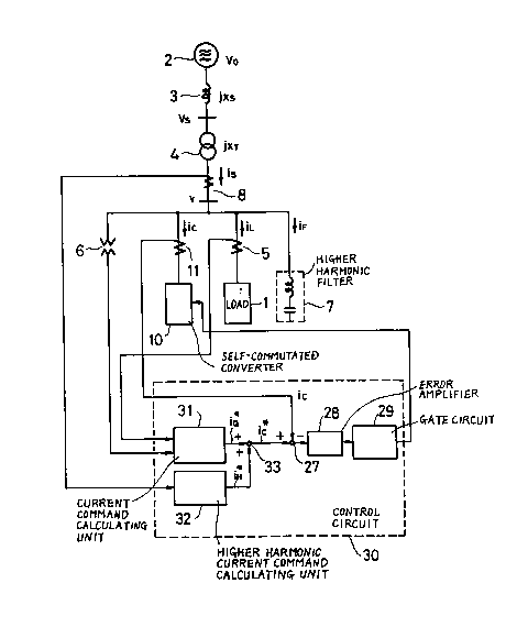
In this invention, as shown in Fig. 1, a control
circuit 30 of the self-commutated converter 10 is equipped
with a current command calculating unit 31 that inputs the
load current iL detected by the current transformer 5 and
the system voltage v detected by the transformer 6 and finds
2Q3171 2
a current command value iQ* for suppressing reactive power
fluctuation of the load 1 or fundamental negative phase
sequence current. The control circuit 30 also includes a
higher harmonic current command calculating unit 32 that
inputs current is flowing in the power system 2 detected
by the current transformer 8 and finds a higher harmonic
current command value iH* for controlling high harmonics
flowing out to the power system 2, and an adder 33 that adds
the current command value iQ* found by the current command
calculating unit 31 and the higher harmonic current command
value iH* found by the higher harmonic current command
calculating units 32. The control circuit 30 is constituted
such that the current ic flowing in the self-commutated
converter 10 is controlled through the error amplifier 28
and the gate circuit 29 in response to the deviation
calculated by the calculation circuit 27 between the sum ic*
of these two current command values added by the adder 33
and the current ic in self-commutated converter 10 detected
by the current transformer 11.
In the above construction, the current command
calculating unit 31 calculates the reactive power consumed
by the load 1 from the load current iL and the system
voltage v, and also calculates the fundamental harmonic
current command value iQ* necessary to compensate for the
reactive power. If required, a signal to compensate for the
fundamental negative phase sequence current of the load 1
can be added to the fundamental harmonic current command
2~317~2
value iQ*. The higher harmonic current command calculating
unit 32 detects the higher harmonic current from the power
source current is, and calculates the higher harmonic
current command value iH* necessary to suppress the higher
harmonic current. These current command values are added
by the adder 33, to obtain the current command value ic* of
self-commutated converter 10.
The self-commutated converter 10 is therefore
controlled by the calculation circuit 27, the error
amplifier 28 and gate circuit 29 in the same way as
conventionally, so that a current flows tracking current
command value ic*.
Hereinafter an embodiment of this invention will be
described with reference to Fig. 2, parts which are the
same as in Fig. 1 and Fig. 4 are given the same reference
numerals and a description of them is omitted. The details
of a control circuit 30A including a current command
calculation unit 31A and the higher harmonic current command
calculation unit 32 will now be described.
In the embodiment shown in Fig. 2, the current command
calculation unit 31A is constructred as follows. The
fundamental harmonic reactive power QL is detected by using
a filter 34 to filter the instantaneous imaginary power q
which is output by the reactive power detection circuit 23.
A coefficient circuit 35 multiplies the fundamental harmonic
reactive power QL by a coefficient (-KQ) to find a reactive
power command value QL*. The reactive power command value
-- 10 --
2~31712
QL* is applied to the instantaneous current calculation
circuit 26, which converts it to a current command value
Q* .
Namely, in the instantaneous current calculation
circuit 26 respective current command values iQR*~ iQS* and
iQT* of the current command value iQ* are calculated as the
following equation (8).
~iQSR* = ~ f 1/2 ~ 1 q 1 ... (8)
~ QT - ~-1/2 - 3/2, vd QL
In the higher harmonic current command calculation
unit 32, a higher harmonic current iH is detected by
applying to a filter 43 the current is of the pcwer system
2 detected by the current transformer 8. The higher
harmonic current iH is then multiplied by a coefficient
(-KH) by a coefficient circuit 44, to find a higher
harmonic current command value iH*.
The current command value ic* of the self-commutated
converter 10 is obtained by combining, using the adder 33,
the current command value iQ* and the higher harmonic
current command value iH* found by the current command
calculating unit 31 and the higher harmonic current command
calculating unit 32.
In the embodiment, the construction of the filters 34
and 43 are well known to those skilled in the art, so the
detailed description of the construction is omitted. The
coefficient (-KQ) of the coefficient circuit 35 can be
20~17 1 2
decided based on the capacity of the self-commutated
converter 10 and the maximum reactive power QLma of the
load 1. The coefficient (-KH) of the coefficient circuit
44 can be decided based on the capacity of the
self-commutated conveter 10 and the maximum value of the
higher harmonics generated by the load 1. But as the
decision of the coefficients (-KQ) and (-KH) is clear to
those skilled in the art, detailed description thereof is
omitted.
The voltage fluctuations produced by the load
fluctuations and the higher harmonics emitted by the power
system 2 are therefore suppressed by controlling the
self-commutated converter 10 by means of the calculation
circuit 27, the error amplifier 28 and the gate circuit 29
in accordance with the deviation between the current
command value ic* and the current ic flowing in the
self-commutated converter 10.
Thus, in this embodiment, the reactive power
fluctuations of the load 1 can be rapidly controlled by
open-loop control, so the voltage fluctuations produced by
the reactive power fluctuations can be suppressed very
effectively. Also, the higher harmonics that flow from the
load 1 to the power system 2 are suppressed by closed loop
control, so higher harmonics of the antiresonance frequency
produced by the constant of the higher harmonic filter 7
and reactance of the transmission line 3 can be suppressed,
and the phenomenon of the higher harmonic filter 7
2~317~2
producing increase in higher harmonics can be eliminated.
A good higher harmonic suppression effect is therefore
obtained.
Next, another embodiment of this invention will be
described with reference to Fig. 3. Parts which are the
same as in Fig. 2 and Fig. 4 are given the same reference
numerals and a description of them is omitted, only the
points of difference will be explained.
In a control circuit 30B according to the embodiment
shown in Fig. 3, as a current command calculating unit 31B,
in addition to the reactive power calculating system in
the current command calculating unit 31A of Fig. 2, there
is provided an negative phase sequence power calculating
system. Specifically, in Fig. 3, the load current iL
detected by the current transformer 5 is converted to
two-phase ac by a three-phase/two-phase conversion circuit
36, as in the circuit 21, and the two-phase ac currents id
and iq are supplied to a negative phase sequence power
detection circuit 37, where the negative phase sequence
power is detected. In this case in the negative phase
sequence power detection circuit 37, a calculation is
performed in the equation (3) whereby vq* is inverted
(multiplied by -1), namely in the following equation (9)
[qPN ~ = [i d _ i dq J ~- vdq * ]
where PN and qN are the outputs of the negative phase
sequence power detection circuit 37. The ~vq* employed in
~317~2
this calculation is obtained by inverting the output vq*
of the synchronous detection circuit 24 by menas of an
inverter circuit 45. The fundamental harmonic positive
phase sequence and negative phase sequence powers
constituting the output of the negative phase sequence
power detection circuit 37 are detected as ac of a
frequency multiple of the fundamental frequency and as dc,
respectively. The fundamental harmonic negative phase
sequence powers PN and QN are therefore obtained by
filtering these outputs PN and qN through filters 38 and
39. Negative phase sequence power command values PN* and
QN* are found by multiplying these fundamental harmonic
negative phase sequence powers PN and QN by a coefficient
(-KN) using coefficient circuits 40 and 41, and are applied
to an instantaneous current calculating circuit 42, where
they are converted into a negative phase sequence current
command value iN*. Namely, in the instantaneous current
calculating circuit 42, respective current command values
iNR*, iNS* and iNT* of the negative phase power command
values iN* are calculated as the following equation (10).
iNS*~ 7~ [-1/2 ~ ] l d q 1 ~ Nl (10)
NT ' -1/2 - 2 Vq*-vd J l QN
The negative phase sequence current command value iN*
is then combined with the current command value iQ*
mentioned above and the higher harmonic current command
value iH* by an adder 33B, and output as the current
- 14 -
20317 12
-
command value ic* of the self-commutated converter 10.
In the embodiment, the construction of the filters 39
and 43 are well known to those skilled in the art, so the
detailed description thereof is omitted. The coefficient
(-KN) of the coefficient circuits 40 and 41 can be decided
based on the capacity of the self-commutated converter 10
and square root of (PN2 + QN2 ) . But as the decision of the
coefficient (-KN) is clear to those skilled in the art,
detailed description thereof is omitted.
In the embodiment, the three-phase/two-phase
conversion circuit 36 is provided separately from the
three-phase/two-phase conversion circuit 21. But the
three-phase/two-phase conversion circuit 36 may be
omitted. In this case, the outputs id and iq of the
three-phase/two-phase conversion circuit 21 are applied to
the inputs of the negative phase sequence power detection
circuit 37. Contrary, the three-phase/two-phase conversion
circuit and the synchronization detection circuit may be
provided for negative phase sequence power detection,
separately from the three-phase/two-phase conversion
circuit 22 and the synchronization detection circuit 24.
Thus, the current command calculating unit 31B has a
powerful suppressing effect not only on fluctuations of
reactive power of the load, but also on fluctuations of
negative phase sequence current, owing to the open-loop
control. Its effect in suppressing higher harmonics is the
same as the embodiment of Fig. 2.
2Q31712
As described above, with this invention, the following
benefits are obtained.
(1) The invention is highly effective against even
steep voltage fluctuations, since the voltage fluctuations
produced by load fluctuation are suppressed by open loop
control.
(2) Fluctuating higher harmonics can also be
suppressed since there is no antiresonance frequency as
there is in the case of the conventional higher harmonic
filter, since higher harmonics are supressed by closed loop
control.
(3) There is an economic advantage in that the
capacity of the self-commutated converter can be reduced
because higher harmonics which do not change with time are
absorbed by a higher harmonic filter, and only the
remaining higher harmonics emitted to the power source are
suppressed by the self-commutated converter.
Obviously, numerous modifications and variations of
the present invention are possible in light of the above
teachings. It is therefore to be understood that within
the scope of the appended claims, the invention may be
practiced otherwise than as specifically described herein.
- 16 -