Note: Descriptions are shown in the official language in which they were submitted.
2~31~99
1 UD089009
EJECTOR MECHANISM
Background of the Invention
This invention is directed to a manually operable
ejector mechanism for removing an edge connected printed
circuit board (PCB) from a connector mounted within an
enclosure.
Electrical connection is commonly made with PCB's by
means of a connector jack which receives and engages metal
runners projecting on an extended portion of the PCB. This
connector normally includes a plurality of conductive
spring-loaded contacts that engage each of the PCB
conductors. The compression force applied to the PCB by
the connector contacts provides resistance to slidably
removing the PCB from the connector.
Enclosures are commonly designed to receive a
plurality of edge mounted PCB's. Each PCB typically has a
front panel assembly mounted thereto. A plurality of PCB's
may be grouped together and mounted to a single panel. The
front panels are normally disposed relative to the
enclosure in the operational ~engaged) position such that
it is difficult to directly grasp the panel and remove the
attached PCB's.
This problem can of course be addressed by mounting a
conventional fixed handle to the front panel. However,
this is not desirable in all installations. It is also
known to provide a pivotally mounted lever to the PCB
assembly where one end of a sub~tantially straight lever
can engage a fixed element of the enclosure to provide a
mechanical advantage to urge the PCB assembly from the
connector. This mechanism provides relatively satisfactory
results when utilized with a single PCB with a front panel.
The use of two or more PCB's mounted to a single front
panel often renders such a lever having a single fulcrum
ineffective. The single force application point provided
~ 2~31~9~
2 UD089009
by such a lever, especially in a multiple PC~ assembly,
often does not supply an optimal removal force.
It is an object of the present invention to provide an
improved ejector mechanism especially suited for removal of
multiple PCB assemblies.
Brief Description of the Drawings
Figure 1 is an exploded isometric view of an
embodiment of an ejector mechanism in accordance with the
present invention.
Figure 2 is a cross-sectional view illustrating a PCB
assembly which incorporates an embodiment of the present
invention engaging a connector in a enclosure.
Figure 3 is similar to Figure 2 but with the
embodiment of the ejector mechanism shown in its operative
position having moved the PCB assembly forward to disengage
the connector.
Detailed Description
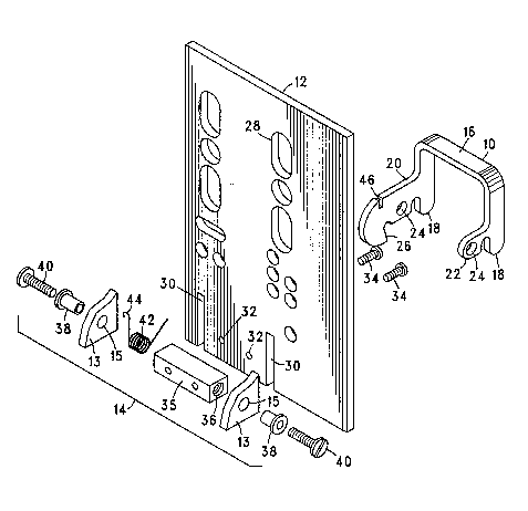
Figure 1 is an exploded view showing an ejector 10
according to the present invention in relationship to a
front panel 12 and two PCB's 13. A mounting assembly 14
attaches ejector 10 and the PCB's 13 to panel 12. Ejector
10 preferably consists of a U-shaped rigid element having a
handle portion 16 and two legs with rounded distal ends 18.
The two leg portions of handle 16 contain lateral
projections 20 and 22, respectively. Each of these
projections have a hole 24 which serves as the pivot point
for the ejector. Preferably, the pivot point is disposed
nearer ends 18 to provide a mechanical advantage.
Projection 20 preferably includes a projecting abutment
surface 26 which enables the ejector to lock the front
panel 12 in an engaged position, i.e. with the PC~'s
engaging the connectors.
' .
.' ' ' ' .
2~3~99
3 UD089009
Front panel 12 which is preferably formed of metal may
include a plurality of holes 28 disposed to accommodate
displays, switches, and other functions associated with
each PCB. Slots 30 are disposed to receive projections 20
and 22. Holes 32 receive screws 34 to mount the assembly
to panel 12.
The mounting mechanism 14 serves to mount the ejector
10 to panel 12 and may ser~e to assist in mounting the
PCB ' s 13 to panel 12 via holes 15. Threaded holes 36 in
opposing ends of mounting block 35 each receive a screw 40
which secures a busing 38 thereto. A spring 42 mounts
about busing 38 in the end of block 35 adjacent ejector
projection 20. A bent end 44 of spring 42 is disposed to
engage a notch 46 in projection 20 in the assembled
position and provides a normal bias causing ejector 10 to
be biased to the position as shown in Figure 2. The other
end of the spring engages panel 12.
In order to maximize the functionality of mounting
block 35, preferably the two PCB ' s 13 each have holes 15 in
the lower front corner and are secured to block 35 between
the bushings 38 and screws 40 thereby securing the printed
circuit board to panel 12.
Figure 2 illustrates a cross-sectional view of ejector
10 mounted to PCB ' s 13 and panel 12. This assembly is
shown engaging electrical connector 54 within an enclosure
48. This enclosure preferably includes a guide 50 which
guides the lower edge of PCB 13. This facilitates
engagement of projecting portion 56 of the PCB with rear
mounted electrical connector 54. This establishes
electrical connections with the PCB in a well-known manner.
However, any mating jack and connector could be used to
establish the electrical connections.
It will be apparent that Figure 2 illustrates only one
PCB board 13 which is mounted adjacent projection 20.
Another PCB 13 is mounted adjacent projection 22 as seen in
Figure 1. Enclosure 48 preferably includes a stop 58
disposed to be engaged by abutment surface 26 when the PCB
,
,
,
.~ .
2~3~99
~ UD089009
assembly is in its operative condition as shown in Figure
2. Spring 42 provides a bias causing ejector 10 to be
biased counterclockwise as seen in Figure 2 and thereby
cause abutment surface 26 to engage stop 5~. This
constitutes a lock mechanism to prevent accidental
disengagement.
Figure 3 shows that ejector 10 has been manually moved
from the operational position as shown in Figure 2 to the
ejected position as shown in Figure 3. Projection 56 of
PCB 13 has been moved forward and no longer engages
connector 54. This action was caused by the translational
force exerted upon panel 12 when handle 16 was rotated
clockwise as shown in Figure 3. This causes distal ends 18
to engage a forward surface 60 of enclosure 48. The
rotation of ejector 10 causes abutment surface 26 to
disengage stop 54 permitting the PCB assembly to slide
forward (to the right as shown in Figure 3). Distal ends
18 are free to pivot through slots 30 in panel 12 and
engage surface 60 simultaneously thereby providing two
spaced apart points for force application. Each of the
force application points apply a force substantially
adjacent each PCB and serves to transfer a substantially
translational force to each PCB.
This should be contrasted with a single lever which
provides only a single point of force application which
would not be substantially in the plane of the PCB's. The
ejector according to the present invention applies separate
forces substantially in the plane of each of the PCB's and
thus tends to minimize the transmission of undesired torque
and maximize the desired in-line force to the PCB's.
In a preferred embodiment according to the present
invention each of a plurality of PCB's mounted to a common
panel would have an adjacent point of force application
applied by means of a corresponding distal end of an
ejector. For example, in a three PCB assembly, the ejector
could be similar to that shown in Figure 1 but include an
additional center leg to form an ~Iml~ which would provide a
:'
.
2~3~9
.,
UD089009
distal end for each of the three PCB's and thereby maximize
the application of force in accordance with the present
invention. Alternatively, the U-shaped ejector as shown in
Figure 1 could be used with more than two PCB's by
disposing each leg adjacent the outside PCB's thereby
relying on the front panel to supply force distribution to
the interior PCB's.
A further aspect of the present invention resides in
the economies of attaching the ejector, the PCB's, and the
front panel utilizing a common mounting assembly 14. This
minimizes the number of parts required and enhances
manufacturability.
Although embodiments of the present invention ha~e
been shown and described herein, the scope of the invention
is defined by the claims which follow.
- .,
.