Note: Descriptions are shown in the official language in which they were submitted.
WO 90/13807 ~ d ~ ~ PCr/US~0/02598
Optical Sensor ~or Detecting Qu;3ntity o~ Protective Goating
2 Statement o~
3 Governmental Interest
4 The United States government has right ;n the present invention pursuant to
Air Force Systems Command Contract No. F33615-86-C~50a,4, entitled "Robotic
6 Paint Stripper Cell (RPSC)". The United States governrr~ent has a nonexclusive,
7 nontran~sferable, irrevocable paid up license to practice or have practice for or on
8 behalf of the United States this invention throughout the world.
9 Field of
l 0 the Invention
11 The present invention relates generally ~o optical sensors. More
12 specifically, the present invention provides an improved optica~ sensor for de~ecting
1 3 the quantity of a protective coating, such as paint, which is deposiled on a surface.
1 4 Background
Protective coatings such as paint serve many purposes, including protection
1 6 from moisture, sunlight, and other environmental conditions. On military aircrafl,
17 protective coatings, including various types of paint, are used to form camou~lage
18 patterns to make the aircraft less visible. New coats of painl are often applied to
I 9 change camouflage patterns or to change unit insignia patterns which aircraft move
20 from one squadron or region of the world to another. Furthermore, new coats of
21 paint are applied periodically to improve the appearance of the aircrafl. Since i~ is
WO 90/13~07 ~ JS90/025~8
~ ~ ~ ?. ~
much easier in field operation to simply put another coat of paint on top of existing
2 paint, il is not uncolrmlon to find that, as years go by, rntlitary aircrnft of~en have as
3 many as 12 con~s of paint. Eventually, the weight of lhis paint is sufficient to effect
4 the op~rationa] characteristics of tile aircraft.
Paint and other protective coatings must be removed fron~ aircraft in order to
6 allow detailed surface inspection, to perform other rework and repair operations,
7 and to keep the weighl of the aircraft within acceptable levels. In the past, pain~
8 removal procedures have employed chemical paint strippers for removing paint.
9 However, as environmenta] awareness has increased, the COSI of disposai of toxic
cllernicals such as phenols has become prohibitive.
1 1 Recenlly, there has been major interest in finding an economical
1 2 environmelltally safe subs~ e for chemical paint stripping. One proposed melhod
] 3 involves plastic media blasting (PMB), which involves blastin~ the surface of an
14 aircraft with small plastic pellets in--a manner similar to sandblasting. PMB is
currently used in manual installasior~s in a number of military and commercial
16 operations. The resulting was~e material is much less toxic t~l~n phenol or other
17 chemical strippers. However, PMB methods require maulipula~ion of very heavy
18 hoses whi]e stnnding on ~t ai-crafl wing covered with a layer of plaslic beads.
19 Such conditions crcate a high potential for loss of footing, Ihus representing a
2 0 hazard to the opera~or.
21 Determining Ihe amount of paint covering a surface is not an ea.sy task.
2 2 The task is compIicated by the fact that many different color.s aud patten~s of paint
2 3 are used on several different types of substrate materials. In many cases ~4hite or
2 4 silver paints are used on aluminum, dark-blue or black decals a.~ placed over paint
in places where the aircraft substrale malenal is black and graphite-epo.Y~
26 compo~ite. In addition, the sensing must be performed as the plastic bends are
WO 90/13807 2 ~ ~ ?. !~ 3
being blasted on the surface, with the air hazy from paint dust, and with the paint
2 pattern continually changing.
3 Sensing the amount of paint on the su:~face of the aircraft is not an easy task
4 even for human ~pcrators. When they see a dark area in a white region it is often
difficult to distinguish dark decal over white paint from a ~egion where white paint
6 has been stripped off a composite surface. Operators often combine prior
7 knowled~e of the surface to reach decisions. For example, if the dark area appears
8 in a region where they have not yet blasted, they will assume it is a decal. On the
9 olher hand, if it occurs in a regjon where ~hey have blasted and saw white earlier,
they wi]l assume the dark area to be a black composite substrate.
11 Ideally, the PMB process should be fully au~omated to remove human
12 operators from the aforementioned hazardous environment. Such an autornated13 system would involve the use of large robotic systems comprising sensors which
14 are capable of obtaining consistent and satisfactory results. A major prob]em
associated with such paint stripping robot systems is the ability to conlrol the1 6 stripping process. Control of the process requires knowledge of how much of ~he
17 paint has been removed and how much of the paint remains on the surface. lt is
18 apparent therefore, that such an automated system requires a sensor which is
] 9 capable of detennining lhe amount of paint remaining on the surface and which can
withstand a harsh b]asting environment.
90/13807 RCr/US90/02S98
Su~y .~ ~J
2 the~'lnvéntion
3 The presenl invention overcomes the difficulties of the prior art by
4 providing an optical sensor which can be used in conjunctiol) with an automatic
5 stripping apparatus that is con~o]Jed by a ro~oLic system. In the sensor of the
6 present invention, a plurality of sensing elements are placed in a prede~ermined
7 geometrical relationship with respect ~o a plurality of nozzles which deliver the paint
8 stripping materia~. F~ctl of lhe sensing elements comprises a lens system which
9 optimizes inspection of the desired ~ie~d of view while minirnizing the effects of
10 light fTom outs;de thc ~Iesired ~ield of view. The sensing elemellts produce optical
1 1 signals which are converted into electrical signals by a plurality of optical detectors.
12 The optical detectors are coupled to the opticDI sensing elements by a plurality of
1 3 optic~l fibers. Each of Ihe deteclors comprises two photosensitive devices, such as
14 photodiodes, to provide elec~rical signal represenlations of the condilion of the
I 5 surface to be stripped. A bandpass filter is placed in front of each of the
I 6 photodiodes. The center wavelengths of the bandpass filters are separated by a
I 7 large enough range ~o ensure effective operation of the sensor.
18 The signal OlJtpUt of the plurality of delectors is analyzed using a
I 9 programmable digital computer which is used to control a robotic positioning
20 system. In the preferred embodiment of the present invention, four sensing
21 elements are aligncd in a linear pattern to obtain inforrnation relating to the blasl
2 2 stream. In addition~ first and sec ~nd c~libration sensing elemen~s are posilioned lo
23 provide refeTence signals for use by the four sensing elements in the blast stream.
24 Reference signals corresponding to protective coating and bare substrate are
25 obtained by positioning the calibration sensors over a pure sample of protective
26 coating, such as paint, and over bare substrate, such as a]uminum. The firsl
27 sensing element is positioned ahead of the row of blast nozzles and the second
WO 90/13807 PCr/US90/0~598
2 ~3 ?; 2 ~
sensing element is positioned behind the row of blast nozzles. Under normal
2 operating circumstances, the first sensing element will see only protective coating
3 and the second calibration sensing element will see only bare substrate.
WO 90/13807 2 ~ , Lt. 9 ~ 6 PCr/US90/02598
Brief Description
2 of the Drawings
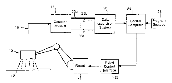
3 FlG. I is a schematic block diagrarn showing the optical sensor of the
4 present invention in conjunctiorl wilh dala processing equipment and a robotic
S posilioning syslem.
6 FIG. 2a is a perspeclive illustration of the s~ripping head showing the
7 placement of nozzles for delivering the stripping ma~erial an~ the placement of the
8 optical sensingelements.
9 FlG. 2b is an illustration of the relative placement of the sensing ~elds and
.
10 the blast fields for the elemcnts sl~wn in FlG. 2a.
1 1 FIG. 3 is an elevational cross sectional view of a sensing element used in
] 2 the present invention.
13 FIG. 4 is an elevational cross sectional side view of one of the detectors
14 used in ~he optical sensor system of the present invention.
FIG. 5 is a process flow chart showing the processing steps implemented
16 by ~he process con~rol algorithm of the present invention.
, ~ ~ , ::
.. , ~ ~ :
~: :
,: :
,...
.
,
.
: . - .
.. . . .
,.. .
. :
~', ' . .
" '
Wo 90/13807 ~;7 2
t:)etailed Descriptiorl oS
2 the Preterred Embodim~nt
3 Referring to F]G. 1, a schematic block diagram is sllown of a stripping
4 system employing the optical sensor system of the present invention. A stripping
5 head assembly 10 is shown positioned over a portion of material or "substrate" 12
6 to be stripped. The dashed lines shown in FIG. I represent the field of view of the
7 optical sensoTs, discussed i~ grea(er de~il below. llle blast pattern of the stripping
8 material is approximately the same as the field of view of the center row of sensors
9 shown in FIG. 1. The position of the stripping head is controlled by a robot 14.
All physic~l nlaterials exhibit a unique reflectance spectra over the optical
1 1 wavelengths spanning ultraviolet through infrared. In particular, the optical
12 refleclanc.e .spectra of paint and aluminum differ in the amount of infrared ligh~
13 absorbed and the amount reflected. Paint ~particularly the polyurethane based
4 paints used on aircraft) absorbs more light and reflect less at longer wavelengths.
15 Carefu] nleasurement of the absorption or reflectance SpeCIra can be used to
1 6 differentiate a protcctive coating, such as paint, ~rom the underlying substrate.
17 'Ihe disadvantage of complete spectral analysis is Ihe time required to
1 8 measure reflectance at a large number of wavelengths, compare Ihe spectral p tttern
I 9 eo patterns Or known materials, and then deterrnine the type of material. The time
20 required can be reduced by measuring at a smaller number of optical ~ aveleng~hs
21 provided the refleclance characteristics of Ihe materials are sufficiently different at
22 the wavelengths selecled. The sensor described here is based Ol~ the measurement
2 3 of reflectane~ at two wavelen~ths.
24 As will be discussed in greater detail be]ow, two electro-optic sensors are
25 used~ one to measure the reflected light in a spectral band centered at a wavelength
26 of 900nm and the other in a band centered at 1700nm. This separation in
27 wavelength has proven to provide an adequate difference to distinguish between
~ PCI/US90/02~98
paint and substrates. The reflected light in each wavelength range sample can be2 determined by optical bandpass filters with center passbands at wavelengths
3 speci~led or by con~binations of high and low pass optical filters. Because Silicon
4 de~ectors operate very well in the near infrared region, they are used for the ]700nm
wavelength. Other types of detectors, such as Lead-Sulfide and Aluminum-
6 Gallium-Arsenide. covld a3s<~ be used for these measurements.
7 The stripping head 10 contains a plurality of sensing elements, discussed in
8 greater detail below, which are used to obtain inforrnation relating to the percentage
9 of pain~ o~ otlle~ p~otective coating remaining on the substrate. The outpul of the
sensing elements is carried bv a fiber optic bundle 16 which is connected to a
1 I detector module 18, comprising a plurality of individual detector elements,12 discussed below in connectioll with FIG. 4, which are operable lo convert the
1 3 optical signals from each of the sensing elements into a voltage signal which can be
14 transferred to a data acquisition system 20. As will be discusscd below, each of the
detector elements comprises two photosensitive devices, such as photodiodes.
16 Therefore, each of the detector elements will produce two outpu~ voltages
17 representing fil~ered optical signals. The respective pairs of output signals are
1 8 illustrated genera]ly by reference numerals 22a~22c.
1 9 The signals received by the data acquisition system 20 are converted, using
techniques known in the art, into data signals which can be used by control
2 I compu~er 2~ e control compu~er l3.se.s ~n algorithm stored in progTam storage 26
2 2 to process the data signals to determine the effectiveness of the stripping process
2 3 and to provide appropriate control signals to robot con~rol interface 28. The robot
24 14 can thus be controlled to move the stripping he~td 10 over 1~e surface 12 in a
2 5 manner to optimize the stripping process.
2 6 Referring to FlG. 2a, a perspective view of the stripping head is shown to
2 7 provide infonmalion relaling to ~he placemen~ o~ tl~e opacal sensinl! elemenls rela~ e
`'
WO 90/13807 9, 2 Q 3 2 ~ ~ fi Pcr/US90/02~98
to the nozzles for delivering stnpping material. As was discussed above, one
2 popular me~llod for s~rippil~g protective coatings, such as paint, is the use of plastic
3 media blasting (Pl-IB), which involves blasting the surface with small plastic yellets
4 in a manner similar lo sandblasting. The present iisclosure does no~ provide details
relating to the operation of the PMB systern, since such systems are well known in
6 the art.
7 In the preferTed embodiment of ~he present invention, PMB rnaterials a}e8 delivered throu~h nozzles 30a, 30b, and 30c, which are aligned in a linear patlern
9 within the stripping head, as shown in F~G. 2a. First and second optica1 calibration
l 0 sensors 32a and 3'b, respectively, are positioned in the stripping head to provide
I ] reference signals w hich can be used lo determine the effectiveness of the s~npping
l 2 process. For purposes of discussion, optica] sensing element 32a will be referred
I 3 to as tlle front calibralion sensing element and element 32b will be referred to as the
1 4 rear calibration sensing element. Light to illuminate the surface I2 is provided by a
l 5 plurality of light sources 34a-34d arranged in a pattem to provide uniform lighting
16 of the surface l2. In the preferred embodiment of the invention, the light sources
I 7 are halogen bulbs which produce in~rared-rich light.
I 8 FIG. 2b is an illustration of the operational field of each of ~he nozzles 30a-
l 9 30c and the optical sensors 32a-32e. - For example, the front calibration field would
2 0 correspond to the optical field of view for optical sensing elemeilt 32a and the rear
2 l calibration field would correspond to the field of view for rear calibration sensing
2 2 element 32b. The left and right center sensor fields correspond ~o the fields of view
2 3 for optical sensing elements 32e and 32d, respectively. Finally, the left and right
24 sensor fields correspond to ~he field of view for sensing elenlents 32f and 32c,
2 5 respectively. The cen~er blast field corresponds to the stripping field for nozzle 30b
26 and the center blast field and left blast field correspond to the stripping area for
27 nozzle 3()a and 30c, respective1y. The information obtained from each sensor
WO 90/13~07 PCr/US90/02S98
,~,r~ /0
element is the average over the field of view for that element. This average signal
2 value can be compared to reference calibration signa~ values for paint and bare
3 substrate, to obtain a quantitative estimate of the percentage of coating remaining on
4 the substrate.
The sensing elements 32a-32f are idenlical to one another, wi~h each
6 element having the components shown in FIG. 3. ~he sensing element, designated
7 generally by reference numeral 32, is contained in a generally tubular housing 40
8 having a protective lens 42 attached on one end thereof. A lens element is adapted
9 to TeC~ e li~h~ Ihrou~h the protective lens and to focus the optical image through an
I O apcrture 46 onto the terminat~on of a fiber optic cable 48 for transmission to the
I I detector elements contained in the detector module 18. The lens system of the
12 preferred embodiment is designed to narrou the ~leld of view of the sensor 10
1 3 approximately the sile of the blast pattern, while gathering a large amount of light
14 renected from the surface 12~ The aperture 46 serves to eliminate light rays coming
15 into the syslem from outside the desired fi~ld of view~ Thç size of the aperture
1 6 determines the amount of light which will be gathered by the sensor~ The distance
1 7 of ~he lens from the fiber bundle affects the amount of lighs which will be gathered
1 8 by the fiber cable. Although more light is gathered as the dis~ance is decreased, the
19 fiber bundle cannot be moved too close to the lens or none of the light will be
2 0 gathered. The system has been optimized to insure maximum transmission of light,
21 within the constraint posed by the distance between the blast nozzles. In the
2 2 preferred embodiment of the invention, the lens assembly has an outer diameter of
2 3 approximately one inch.
24 Refcr~ing again to FIG~ 1, the fiber optic bundle 16 comprises a plurality of
2 5 fiber optic cables 48 of the type shown in nG. 4~ The optical signals transmitted in
26 the fiber optic cables are converted into electrical signals by a plurality of detector
27 elements con~ained in the detector module 18 FIG S is a cross sectional view of a
;~:
.~
:
wo go/1~t~07 ~ q ~3, P~/US90/02598
detector element of the type employed in the presenl invention. The fiber optic
2 cable 48 containin~ ~he signal from the optical sensing element 32 is connected to
3 the housing 50 in an appropria~e manner. The ligh~ signal ernit~ed by the fiber optic
4 cable 48 is focussed by a collimating lens 52 which is operably connected ~o the end
of cable 48. The focussed light beaun is direc~ed toward a beam split~er 54 to direcl
6 a portion of ~lle optical signal toward first and second detectors 56 and 58,
7 respectively. A first optical filter 60 is secured within a mounting bracket 62 to
8 fil~er ~he portion of ~he ligh~ beam de~ec~ed by optical detector 56. Likewise, an
9 op~ical filter o4 is sccure within mounting bracke~ o filter ~he portion of the light
beam detected by optical detec~or 58.
l I In order to ensure effec~ive opera~ion of ~he sensor, there mus~ be a
I 2 compara~ively wide separa~ion between the waveleng~hs of thc first and second
l 3 detcc~ors. In the preferred embodimen~ of ~he invention, sensors capable of
14 opera~ing in the infrared region are employed. ln the preferred embodimen~ of ~he
l 5 inven(i~n, ~he firs~ optica] sensor 56 is a silicon pho~odiode and the second op~ical
16 sensor 58 is a gertrtanium pho~odiode. The silicon and germ tnium pho~odiodes
l 7 have a comparatively large difference in their operating wavelengths, thus
18 improvin~ the distinc~ion between the lespective optical signals for paint and
l 9 substrate. The first optical filter used in the preferred embodiment is an 800
nanomeler hi~hpa~s fi1ter. Tl~e second optical fil~er is a 1600 nanomeler highpass
21 fil~er. ln ord~ for the sensor system to opera~e properly, the outpu~ of the gain
2 2 stages of ~he germanium and silicon pho~odiodes must be adjusted to comparable
23 vo]tages. Since the sensors do not have the same sensi~ivity, the gain of ~he
24 amplifiers con~ained in the two de~ec~ors mus~ be norrnalized.
The material reflec~ing ligh~ in~o the sensor can be identi~led by ~he rela~ive
26 amplitudes of the signals from ~he 900nm and 1700nm detectors. To de~ermine ~he
2 7 rela~ive arnpli~udes, the output voltage of the gain amplifier for the long wavelength
wo 90/l3~ . A ~; ~ Pcr/usgo/02598
/~
sensor is divided by the sum of the output voltages of the gain ampli~lers of both
2 the shPrt and long wavelength detectors. This ratio is independent of the intensity
3 of the illuminating light source and can be used to determine lhe type of material
4 reflecLing ~he light.
SThe sensor must be calibrated to compensate for the spectral ernission of the
6 illuminating light source. This is done by placing tl~e .~ensor.~o that its ~leld of view
7 contains a typical paint sample. An average of several ratios is talcen and stored as a
8 typical paint ratio. The sensor field of view is then set to contain a typical substrate
9 sample. An average of several ratios is again t~ken and stored as a typical substTate
1 0 raLio A ileld of view ~hat contains part paint and part substIate will have a ratio that
1 ] falls somewhE~e be~ween the 811 p~ni ;~nd ~he all substrate ratios. The amount of
2 difference between the two calibra~ion ratios will provide the percentage of painl or
13 aluminum. For example, if the paint ratio was 0.200, the aluminum, ratio was
140.500 and the sampled ratio was 0.350 the sensor would be looking at half paint
1 5 and half aluminum. This effect is achieved because the sensor detects the average
1 6 intensity at each of the wave lengshs in the field of view. To control lhe process in
17 real fime, the first and second calibration sensors are used to calibrate for small
18 variation in the surface due to changes in the paint, substratc or environment. The
] 9 leaùlng sensor will. `see ' a.~l pain~ and the t~ailing sensor will "see" all substrate.
2 0FIG. S is a tlowchart representation of the processing steps implemented by
21the system control software. In steps 100 and 102, the signal levels are deterrnined
22 for each of the germanium and silicon sensors in the detector elements. In step
2 3 104, the value of fhe signal level of the germanium sensor divided by a value equal
2 4 to the sum of the cornbined values of the signal levels for the gennanium and silicon
25 sensors. This value is an intensity independent ratio directly related to the
2 6 difference between the two sensor values. Once all of the ratios are computed, the
27 percenlage of paint and substrate are deterrnined. This is done by using the
90/13807 2 ~ PCr/USs0/02ss8
/~
calibration sensor ratios to provide information relating to the condition of the
2 surface. Thus, as indicaled in steps 106 and 108, calibration signal level ratios are
3 obtained for the front sensor (pure paint) and the rear sensor (pure substrate). For
4 the ideal case, it is assumed that the calibration sensor that is before the blast
5 nozzles will see only paint and the calibration sensor which is behind the blast
6 nozzles will see only substrate. lf the calibration sensor ratios are too far off the
7 calibration values deterrmned from the samp1e panels, then t!-e calibration values
8 from the sample panels are used by the system. Otherwise, the calibration sensors
9 are used to compare the signal values frorn the sensing elements 33c-33f to
10 detennine the relative percent of paint on the substrate. In step 110, the sigllal leve]
I I ratio for the two center blast sensors is deterrnined and, likewise, this signal ratio is
12 calculated for the t~ o outer bias~ s~ns~rs in step 1:12. In stcp 114, the signal ratio
13 for lhe two inner sensors is compared to a predetennined value and in stcp 116 a
14 deterrnination is made as to whether this ratio is equal to the predetermined value.
15 If i~ is detem~ined that the ratio does not equal the predeten~lined value, then the
1 6 robot speçd is changed in step 118 and the control software returns to reference
1 7 mark A to repe tt steps 110- I 16. However, if it is deterrnined that the ratio is equal
1 8 to the presenl value, then the systern prooeeds to step 120 where the ratio for the
l 9 outer sensors is compared to the predetermined value. In step 122 a detennination
20 is made of whether the ratio is equal to the predctennirled value. If the ratio is not
21 equal to the predetermined value, then the robot speed is adjusted in s~ep 124 and
22 the system again rcturns to step 110. If however, it is detem~ined that ~he ratio is
23 equal to the predeIermined value, the system proceeds to step 126 where a
24 determination is made of ~,vhether the stripping process is completed. If the
2 5 stripping is not completed, the systeln return to step 110.
26 Although the method and apparatus of the present invention has been
27 described in connec~ion with the preferred embodiment, it is not intended to be
WO 90/13807 ~ PCI/US90/02598
limited to the specific form set forth herein, but on the contrary, it is intended to
2 cover such modifications, alternalives and equivalents as can reasonably be
3 included wi~in t~e spirit and scope of the clairns.