Note: Descriptions are shown in the official language in which they were submitted.
NE-302- 1 - 2032 746
TITLE OF THE INVENTION
ARRANGEMENT FOR
TRANSLATING LOGICAL PAGE ADDRESSES
TO CORRESPONDING REAL ONES
IN DATA PROCESSING SYSTEM
BACKGROUND OF THE INVENTION
Field of the Invention
The present invention relates to an arrangement
for translating logical (or virtual) page addresses into
corresponding real ones in data processing systems using
virtual memory techniques.
Description of the Prior Art
A so-called supercomputer has found extensive uses
in high speed mathematical or scientific tasks such as in
weather forecast simulation, image data processing for
natural resources, etc. It is known in the art that such
a very powerful mainframe adopts high-level operations
that work on vectors (viz., linear arrays of numbers)
utilizing a virtual memory technique. The virtual memory
is large imaginary main memory made available by loading
smaller pages from a backing store into a main memory as
they are required.
The mechanism used to define the relationship
between the logical (or virtual) address space that the
program thinks it is controlling, and the actual main
memory locations being utilized, is called a "address
translation".
In order to accelerate the page address
translation, it is a common practice to prepare one or
more address translation buffers into which a page
address translation table(s) has previously been
transferred from a main memory.
One known approach to performing high-speed page
address translation, is to translate all the logical
page addresses at a time by preparing a plurality of
2032 74 6
NE-302 - 2 -
address translation buffers the number of which is equal
to the whole number of logical pages. Although this
method is able to attain the address translation at a
high speed and hence a high throughput, it has
encountered the problem in that a bulky hardware
arrangement is undesirably required.
Another known approach is to prepare a plurality of
address translation buffers and then implement address
translation of a plurality of consecutive logical pages
at a time according to a heading number of the
consecutive logical pages to be translated and a
direction (increasing or decreasing direction) of the
consecutive page numbers. This prior art has been
disclosed in Japanese patent application publication No.
63-62012 issued for public inspection on December 1,
1988. This prior art features an effective address
translation without an undesirable increase in hardware,
but has encountered the problem in that it is unable to
implement address translation of a plurality of logical
pages at any given time if a program requires random
logical pages in the case of indirect addressing.
SUMMARY OF THE INVENTION
It is an object of the present invention to provide
an arrangement for translating logical page addresses
into corresponding real ones without undesirable increase
in hardware.
Another object of the present invention is to
provide an arrangement for translating logical page
addresses into corresponding real ones without referring
to the increasing or decreasing direction of consecutive
logical page numbers to be translated.
In brief, the above object is achieved by an
arrangement by which a predetermined number of logical
page addresses are effectively translated into
corresponding real ones. The number of the logical page
NE-302 - 3 - 2 0 3 2 7 4 6
addresses is determined by (M+N) bits and, each of the
logical page addresses includes upper M-bit and lower N-
bit. Logical page address registers, whose number is
equal to 2N, are provided to respectively store the
predetermined number of logical page addresses applied.
Address translation buffers (whose number is also equal
to 2N) each stores 2M real page addresses which are
grouped according to each of the lower N bits. The
address translation buffers receive the upper M-bit of
one of the logical page addresses, and output real
addresses. An address translation controller receives
the outputs of the address translation buffers and also
receives the lower N-bit, and selects the real page
addresses using the lower N-bit. The selected real page
addresses are applied to a plurality of real address
registers. A page number comparator determines whether
or not the upper M-bit of one of the logical page address
coincides with the upper M-bit of each of the remaining
logical page addresses. The page number comparator
outputs the comparison results which allow the real
address(es) stored in the real address registers to be
applied to a main memory.
More specifically an aspect of the present
invention comes in an arrangement which is provided in a
data processing system wherein a logical address space
is equally divided into a plurality of (M+N) pages and is
accessible by a program, the arrangement being provided
for translating a predetermined number of logical page
addresses into corresponding real page addresses, the
number of the logical page addresses being defined by
(M+N) bits, each of the logical page addresses including
upper M-bit and lower N-bit, the arrangement comprising:
a plurality of first means, the number of the first
means being equal to 2N, each of the first means being
arranged to store 2M real page addresses each of which is
- 2032746
NE-302 - 4 -
defined by one of the numbers determined by N-bit, each
of the first means receiving the upper M-bit of a first
logical page address of the predetermined number of
logical page addresses and outputting a real page address
defined thereby; second means, the second means being
coupled to the plurality of the first means and
comparing the upper M-bit of the first logical page
address with the upper M-bit of each of the remaining
logical page addresses of the predetermined number of
the logical page addresses, the second means outputting
first and second logic signals in the event that the
comparison result indicates consistency and inconsistency
respectively; and third means, the third means being
coupled to receive the real page addresses from the
first means and receive the first and second logic
signals, the third means outputting the real page
address corresponding to the logical page address in
connection with which the second means has outputted the
first signal.
BRIEF DESCRIPTION OF THE DRAWINGS
The features and advantages of the present
invention will become more clearly appreciated from the
following description taken in conjunction with the
accompanying drawings in which like elements are denoted
by like reference numerals and in which:
Fig. 1 is a block diagram illustrating an
arrangement, according to the present invention, for
translating logical (viz., virtual) page addresses into
corresponding real (viz., physical) ones;
Fig. 2A shows a storage format of a logical address
register forming part of the Fig. 1 arrangement;
Fig. 2B shows a storage format of a real address
register forming part of the Fig. 1 arrangement;
Fig. 3 is a block diagram showing in detail, an
address translation buffer which forms part of the Fig. 1
2~3274~
NE-302 - 5 -
arrangement;
Fig. 4 is a block diagram showing in detail, a
page number comparator which is included in the Fig. 1
arrangement; and
Fig. 5 is a block diagram showing details of an
address translation controller which forms part of the
Fig. 1 arrangement.
DETAILED DESCRIPTION OF THE
PREFERRED EMBODIMENTS
A preferred embodiment of this invention will be
discussed with reference to Figs. 1 to 5, in which Fig. 1
illustrates the overall arrangement of the embodiment
while Figs. 2-5 show the blocks of Fig. 1 in detail.
It is assumed that logical address space is
equally divided into (M+N) pages each of which is
specified by (M+N) bits. It is further assumed for the
sake of discussion that M = six (bits) and N = two
(bits). It follows in this particular embodiment that
the number of logical (viz., virtual) pages is 256 (= 28)
while the number of real (viz., physical) pages is 32
(25).
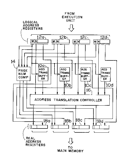
The arrangement shown in Fig. 1 comprises: address
translation buffers 10a, 10b, 10c and 10d the number of
which is 2N (N=2); logical address registers 12a, 12b,
12c and 12d; a page number comparator 14; an address
translation controller 16; and real address registers
18a, 18b, 18c and 18d.
Each of the four registers 10a-lOd is supplied with
a logical address from an execution unit (not shown)
provided outside of the Fig.1 arrangement.
As shown in Fig. 2A, storage format of each of the
logical address registers 10a-lOd comprises a page
portion (M+N = 8 bits) and an in-page address portion 13c
(which is assumed to be 20 bits). The terminology "in-
page address portion" implies in the instant
203274~,
NE-302 - 6 -
specification that a storage portion allocated to the
addresses included in a given page. The page portion is
divided into upper and lower sections 13a, 13b which
occupy 6-bit and 2-bit respectively. The address stored
in the in-page address portion 13c is directly
transferred into the counterpart thereof (viz., l9c) in a
manner which will be referred to later.
Fig. 2B shows storage format of each of the real
address registers 18a-18d. The storage format comprises
an address translation flag l9a (1-bit), a real page
portion l9b (5-bit) and the in-page address portion l9c
(20 bits). In the event that the flag l9a assumes a
logic 0, the content of the corresponding real address
register (18a-18d) is applied to a main memory (not
shown). Contrarily, if the flag l9a assumes a logic 1,
the real address stored in the corresponding register
(18a-18d) is not appliéd to the main memory. It should
be noted that the flag portion of the real address
register 18a always assumes a logic 0, and hence the real
address stored in the register 18a is applied to a main
memory (not shown) without exception.
Fig. 3 shows storage format of each of the address
translation buffers lOa, lOb, lOc and lOd, which are
respectively assigned to N=OO, N=O1, N=10 and N=11.
Further, each of the buffers lOa-lOd is provided with 64
storage sections, denoted by M=OOOOOO, ...., M=111111.
Accordingly, the total number of memory sections of the
buffers lOa-lOd is 256 (= 4 x 64) each of which is
supplied with a real page address from the execution unit
(not shown) and which memorizes same therein. The
numerals 0, 1, 2, 3, 4, ..... , 254, and 255 in Fig. 3
denote the numbers of the memory sections each of which
occupies 5-bit.
Fig. 4 illustrates the page number comparator 14
in detail, which comprises three comparators 14a, 14b and
NE-302 - 7 - 2032746
14c. The upper M-bit (viz., 6-bit) of the logical
address register 12a is applied to all the comparators
14a, 14b and 14c via terminals 17a, 17c and 17e. On the
other hand, the upper 6-bit of the register 12b is
applied to the comparator 14a via a terminal 17b.
Similarly, the upper 6-bit of the register 12c to the
comparator 14b via a terminal 17d while the upper 6-bit
of the register 12d to the comparator 14c by way of a
terminal 17f. The comparator 14a compares the two 6-bit
address data applied thereto on a bit-by-bit basis, and
issues a logic 0 in the event that the two 6-bit address
data applied are coincide. Otherwise, the comparator 14a
produces a logic 1. The other comparators 14b and 14c
each performs the same function.
Fig. 5 shows in detail, the address translation
controller 16 which, in this embodiment includes four
selectors 16a, 16b, 16c and 16d. These selectors 16a-16d
are respectively supplied with the lower page address (2-
bit) of the logical address registers 12a-12d as selector
signals. Further, each of the selectors 16a-16d receives
the outputs of the address translation buffers 10a-lOd.
In the event that the selector 16a receives a bit
sequence N=01 by way of example, the selector 16a outputs
a real page address applied thereto from the address
translation buffer 10b.
The operation of the instant embodiment will now be
described. The registers 12a-12d have already stored
logical addresses applied from the execution unit (not
shown). Merely for the convenience of discussion, it is
assumes that the page addresses (M + N) of the registers
12a-12d are:
Register 12a = 000010(M) + 00(N);
Register 12b = 000010(M) + 01(N);
Register 12c = 000011(M) + 00(N); and
Register 12d = 000010(M) + ll(N).
NE-302 - 8 - 2 ~ 3 2 7 q 6
This means that the page address stored in the register
12c is not continuous with or equal to the other page
addresses in the registers 12a, 12b and 12d. The upper
page bits "000010" in the section 13a of the register 12a
is applied to the address translation buffers 10a, 10b,
10c and 10d. In compliance with the above-mentioned
assumption, the buffers 10a-lOd supply the selectors 16a-
16d of the controller 16 (Fig. 5) with the real page
addresses stored in the memory sections Nos. 8, 9, 10 and
11 (Fig. 3), respectively.
The selectors 16a-16d are also supplied with the
contents of the lower bits (13b) of the registers 12a-
12d, respectively. Since it has been assumed that the
lower bits of the registers 12a-12d is "00", "01", "00"
and "11", the selectors 16a-16d picks up the real page
addresses derived from the memory sections Nos. 8, 9, 8
and 11, and apply them to the real page portions (19b) of
the real address registers 18a-18d, respectively.
As previously referred to, all the comparators 14a,
14b and 14c (Fig. 4) are supplied with the upper M-bit
(viz., 6-bit) of the logical address register 12a. On
the other hand, the upper 6-bit of the register 12b is
applied to the comparator 14a. Similarly, the upper 6-
bit of the register 12c to the comparator 14b while the
upper 6-bit of the register 12d to the comparator 14c.
The comparator 14a compares the two 6-bit address data
applied thereto on a bit-by-bit basis, and applies a
logic 0 to the address translation flag of the register
18b in the event that the two 6-bit address data applied
are coincide. Otherwise, the comparator 14a applies a
logic 1 to the flag of the register 18a. The other
comparators 14b and 14c each performs the same function.
As mentioned above, the flag of the register 18a always
retains a logic 0. A logic 0 in each of the registers
18a-18d allows the real page address thereof plus the
NE-302 - 9 - 2 ~ 3 2 7 4 6
content of the memory portions l9c to be applied to the
main memory. It should be noted that the content of the
memory portion 13c of each of the registers 12a-12d is
directly transferred to the counterpart thereof l9c of
each of the registers 18a-18d.
While the foregoing description described one
embodiment according to the present invention, the
various alternatives and modifications possible without
departing from the scope of the present invention, which
is limited only by the appended claims, will be apparent
to those skilled in the art.