Note: Descriptions are shown in the official language in which they were submitted.
Z~3~3~8
-
SUPER HIGH FREQUENCY OSCILLATOR/RESONATOR
Background of the Invention
Thls invention relates, in general, to resonators and
oscillators, and more particularly to piezoelectric
resonators and oscillators which can be integrated with
other electronic devices.
In the design of radio receivers, particularly paging
receivers, cellular radios, and microwave satellite
communication systems, it is desirable for components which
form the system to take up as little space as possible. It
is desirable for as many components as possible to be
integrated into a single integrated circuit. This
integration also reduces connections needed to make the
radio, greatly improving reliability and reducing
manufacturing cost.
Besides reduced size, higher and higher operating
frequencies have become more common. This has led to the
use of semiconductor materials which can operate in the
gigahertz (GHz) frequency range to be used for the
electronic components. Integrated circuits manufactured in
gallium arsenide can operate at these frequencies. One
problem that is basic to the operation of a high frequency
radio, however, is generation of a high frequency
oscillating electric signal which is used to both transmit
and receive information. Similarly, resonator circuits
which can be used as high frequency filters in the gigahertz
frequency range are needed.
It has been known for some time that certain
crystalline materials have piezoelectric properties.
Specifically, there is what is called a direct piezoelectric
effect, in which electrical charges appear on crystal
surfaces upon the application of an external stress. There
is also a converse piezoelectric effect, in which the
crystal shows strain or deformation when an electrical
charge is applied by external means to faces of the crystal.
A
~3
2 2~33~8
These effects have been used for many years in crystal
oscillators and other devices in which bulk acoustic waves
are transmitted through a crystal, typically between
electrode plates at opposite faces of the crystal.
Usually, quartz crystals are used to make high
frequency oscillators and resonators. These quartz
oscillators are called bulk acoustic wave devices because
acoustic waves are propagated throughout the bulk of the
crystal. However, quartz crystal oscillators cannot be
integrated with other components, and so must be coupled to
other components on PC boards or hybrid substrates. Also,
the technology of quartz crystal oscillators limits their
ability at higher frequencies. Use of bulk waves in this
manner has provided crystal oscillators and filters with
good temperature stability, but with frequencies limited to
about 200 megahertz (MHz) due to excessive capacitance, and
more typically falling below 50 MHz. Consequently, higher
frequencies cannot be obtained without the expense of more
components, such as frequency multipliers. Also, when high
frequencies are derived from multipliers, accuracy and
stability are sacrificed. Because cost, accuracy, and size
of frequency multiplier circuitry is proportional to
multiplication necessary, it is advantageous to use as
little frequency multiplication as possible.
Besides bulk acoustic wave devices, other piezoelectric
devices, also called electroacoustic devices, fall into two
basic categories: surface acoustic wave (SAW) and shallow
bulk acoustic wave (SBAW). As their names imply, each of
the variations refers to the location of the acoustic wave
with respect to a piezoelectric film: at the surface or
just below the surface. Devices using SBAW have become
increasingly popular because they are more stable than SAW
devices and can operate at higher frequencies.
Acoustic waves are generated in a piezoelectric film by
providing an electric field across the film. Since most
piezoelectric films are insulators, it is easy to establish
an electric field across the film. Vertical waves can be
~_ 3 2033318
established by an electric field across opposed surfaces of
a piezoelectric film, while lateral waves can be established
by two electrodes on a single surface. If an oscillating or
pulsing electric field is supplied across the film, an
oscillating acoustic wave will be established. To make an
acoustic wave oscillator/resonator, a standing acoustic wave
must be established in the film. Frequency of the standing
acoustic wave will be a function of device geometry and
physical properties of the piezoelectric material.
Techniques are also known to micromachine silicon
structures to form diaphragms, beams, and cantilever beams
which can then oscillate when an acoustic wave is
established in them. Since silicon is not a piezoelectric
material electroacoustic devices could only be made by
forming a piezoelectric layer on top of a micromachined
silicon structure. These micromachine structures allow
higher frequency operation because of the smaller geometries
used, as the structures can be formed using conventional
semiconductor processing techniques. However, since a
piezoelectric film was deposited on top of a non-
piezoelectric semiconductor structure, even when
micromachining was used the piezoelectric film was supported
by an otherwise quiescent structure. Mechanical coupling
between the piezoelectric film and a non-piezoelectric
material results in damping of the acoustic wave and lowered
quality factor (Q) of acoustic wave filters and oscillators.
Until now, devices which use an unsupported piezoelectric
layer have not been available.
Accordingly, it is an object of the present invention
to provide a method for generating an oscillating current of
very high frequency.
It is a further object of the present invention to
provide a piezoelectric resonator which can be
monolithically integrated with other semiconductor devices.
A further object of the present invention is to provide
a resonator with improved reliability.
4 2033318
-
Another object of the present invention is to provide a
piezoelectric resonator wherein the piezoelectric element is
not supported by a non-piezoelectric material.
Another object of the present invention is to provide
an electroacoustic resonator/oscillator using a
piezoelectric semiconductor material.
A further object of the present invention is to provide
an electroacoustic resonator which uses a Schottky gate to
establish an acoustic wave.
Summary of the Invention
These and other objects and advantages of the present
invention are provided by a method of filtering an
oscillating electric signal wherein a piezoelectric film is
formed on a mechanical support and a portion of the
piezoelectric film forms a beam which extends beyond the
mechanical support so that a cavity is formed underneath the
beam, and the beam is free to vibrate in the cavity at a
resonant frequency when an acoustic wave is propagated in
the piezoelectric layer.
At least one drive electrode is coupled to the
piezoelectric film, and preferably forms a Schottky contact
with the piezoelectric film. A depletion region is formed
under the drive electrode by the Schottky contact. An
unfiltered AC signal is coupled to the drive elec~rode
thereby establishing an acoustic wave when the unfiltered AC
signal comprises a component at the resonant frequency.
Surface charge on the piezoelectric film resulting from
vibration of the beam allows the resonant frequency
component of the unfiltered AC signal to pass through the
depletion region, or alternatively switches a semiconductor
device. Alternatively, the resonant frequency component can
be passed by a tunnel current through the cavity.
20~33~8
_.
Brief Description of the Drawings
FIG. 1 illustrates an enlarged cross-sectional view of
a first embodiment of the present invention comprising a one
port resonator at an early stage of processing;
FIG. 2 illustrates the one port resonator of FIG. 1
further along in processing;
FIG. 3 illustrates a top view of the resonator shown in
FIG. 2;
FIG. 4 illustrates a cross-sectional view of a second
embodiment of the present invention comprising a two port
resonator;
FIG. 5 illustrates a top view of the two port resonator
shown in FIG. 4;
FIG. 6 illustrates a cross-sectional view of a third
embodiment of the present invention comprising a resonator
with gain; and
FIG. 7 illustrates a top view of the resonator of FIG.
6.
Detailed Description of the Drawings
FIG. 1 illustrates a highly simplified cross sectional
view of a first embodiment of a piezoelectric resonator of
the present invention at an early stage of processing. It
should be understood that many variations of this basic
structure are possible and can be easily envisioned which
use the method of the present invention. The piezoelectric
resonator can be manufactured as a discrete component, or as
will be seen, integrated with other electronic devices on an
integrated circuit to achieve either a tuned amplifier or an
oscillator function. A tuned amplifier is provided by
adding a gain structure to the resonator while an oscillator
is achieved by adding gain and appropriate feedback to the
resonator. A first and second embodiment will be described
which are adapted to function as resonators, while a third
embodiment illustrates a resonator with a tunneling gain
~_ 6 2 0~ 3 3 1 8
element. The three embodiments differ very little
structurally, but illustrate various modes of operation of
the present invention.
In the first embodiment, semiconductor layer 11
comprises a semi-insulating or highly resistive layer, and
comprises a III-V compound material such as gallium
arsenide. Gallium arsenide is useful because other high
frequency devices can be manufactured on the same layer and
well-known semiconductor processing techniques can be used
to manufacture the resonator structure. Semiconductor layer
11 can be formed on another semiconductor or semi-insulating
substrate by epitaxial growth techniques.
Semiconductor layer 14 is formed of doped semiconductor
material in the first embodiment. Semiconductor layer 14 is
formed as a continuous layer covering semiconductor layer
11. Piezoelectric layer 13 is formed covering beam support
14. Piezoelectric layer 13 is patterned and etched using
conventional semiconductor techniques. As will be seen, it
is necessary that piezoelectric layer 13, is differentially
etchable with respect to semiconductor layer 14. This is
easily done when semiconductor layer 14 comprises gallium
arsenide (GaAs), and piezoelectric layer 13 comprises
aluminum gallium arsenide (AlGaAs) or similar semiconductor.
Other piezoelectric layers may be used for piezoelectric
layer 13 so long as a suitable material is chosen for beam
support 14.
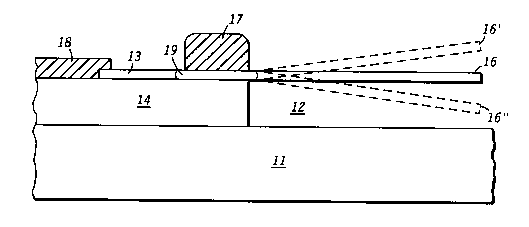
FIG. 2 illustrates the structure of FIG. 1 further
along in processing. After piezoelectric layer 13 has been
patterned and etched, semiconductor layer 14 is selectively
etched to undercut piezoelectric layer 13. This etch leaves
cavity 12 under beam portion 16 of piezoelectric layer 13.
Beam 16 is free to vibrate in cavity 12, as indicated by the
deflected beams 16' and 16'' shown in phantom.
Electrode 17 forms a Schottky contact to piezoelectric
layer 13, and is formed adjacent to beam 16. Electrode 18
forms an ohmic contact to mechanical support 14, and is
formed away from beam 16. In the first embodiment a voltage
7 2~333~8
may be applied to electrode 17 by bias supply 22, shown in
FIG. 3, so that the Schottky contact is biased during
operation. The reverse biased contact results in a semi-
insulating region 19, shown in FIG. 1 below electrode 17,
and establishes an electric field across piezoelectric layer
13. When a Schottky contact is used, semi-insulating region
19 is merely a depletion region of the Schottky contact when
it is reverse biased. With proper design a zero bias
depletion depth of the Schottky contact may eliminate any
need for bias supply 22. This depletion region allows an
oscillating electric field, also called an excitation field,
to be established across piezoelectric layer 13. Electrode
18 may contac~ piezoelectric layer 13 since a depletion
region 19 prevents current flow from electrode 18 to
electrode 17.
Formerly, piezoelectric semiconductors have not been
used as acoustic wave resonators or oscillators because of
the difficulty in establishing the excitation field across
them, but the use of depletion region of a Schottky diode
solves this problem. In addition to a depletion region,
other related techniques can be used, such as proton
implantation underneath contact 17 which converts
semiconducting AlGaAs or GaAs to semi-insulating material.
Only by converting a portion of piezoelectric layer 13 to an
insulator, or by depleting carriers from that portion, can
the excitation field be established.
FIG. 3 illustrates a top view of the resonator shown in
FIG. 2. Beam 16 is preferably about 1 micron by 1 micron,
and extends out over cavity 12. Electrode 17 is formed near
an edge of beam 16 on top of mechanical support 14, which
cannot be seen in FIG. 3. Interconnect 15 couples electrode
17 to an external signal 21 and bias voltage 22. As set out
hereinbefore bias voltage 22 may be supplied by the zero
bias potential of the Schottky contact, and an actual
voltage supply may not be necessary. Several electrodes 17
may be formed coupled to piezoelectric layer 13, although
only one is shown. In the first embodiment, electrode 17 is
8 20333~8
coupled to a DC bias 22 which keeps the Schottky contact
reverse biased during operation. Electrode 17 is also
coupled to an oscillating signal 21 which establishes a
vibration in cantilever beam 16. Oscillating signal 21 may
be a signal picked up by an antenna coupled to the
resonator, for example.
Techniques for forming and placing electrodes 17 to
maximize piezoelectric coupling to beam 16 are well-known,
as are techniques to form electrodes 17 which excite shallow
bulk acoustic waves (SBAWs) instead of surface acoustic
waves (SAWs). SBAWs are preferable to SAWs because such
devices have longer usable lifetimes and are not
significantly effected by contamination or aging of
piezoelectric layer 13.
Instead of a cantilever beam, beam 16 can be formed as
a fully supported beam as shown in a second embodiment
illustrated in FIGS. 4-5. Similar techniques can be used to
form a diaphragm in place of beam 16. All reference numbers
in FIG. 4 and FIG. 5 are the same as analogous structural
elements in FIG 2 and FIG. 3. As illustrated in FIG. 5,
when a full beam is used it is convenient to form electrodes
17 at opposite ends of beam 16, allowing greater flexibility
in layout of electrodes 17. One of the electrodes 17 is
used to excite a SBAW in beam 16, while the other is used to
sense the SBAW and convert its mechanical energy into an
electrical signal. DC bias 22, shown in FIG. 3, has been
omitted from FIG. 4 and depletion regions 19 are formed by
the zero bias potential of the Schottky contacts 17. The
unfiltered AC signal 21 (not shown) is applied to one port
23 while the other port 23 is used to detect a filtered
output. Although fundamental frequency and harmonic
frequencies will be different when different oscillating
structures are used, the basic principle of operation will
be the same for either a cantilever beam (FIGs. 2-3) or a
fully supported beam (FIGs. 4-5). Operation of the present
invention is described for the cantilever beam structure
only.
9 Z(~333~8
The structure shown in FIGs 2-3 serves as a series
resonant structure. Beam 16 has a resonant frequency
determined by its geometry. When unfiltered AC signal 21
comprising a component at the resonant frequency is applied
across semi-insulating region 19, beam 16 vibrates at the
resonant frequency. Unfiltered AC signal 21 may have a low
signal to noise ratio and be, for example, a signal from an
antenna. Unwanted signals which are of a different
frequency than the resonant frequency will have minimal
effect on the oscillation of beam 16. The vibration of beam
16, particularly near the edge of mechanical support 14,
results in an oscillating surface charge forming on top and
bottom surfaces of piezoelectric layer 13, near the
supported edge of beam 16. This surface charge oscillates
at the resonant frequency and effectively passes the signal
at the resonant frequency through depletion region 19
piezoelectrically. Since only components of unfiltered AC
signal 21 which are at the resonant frequency can pass
through depletion region 19, the AC signal is filtered.
Other semiconductor switches can be used in place of
the Schottky contact. For example, a bipolar transistor
having the base driven by piezoelectric layer 13, or a field
effect transistor having a channel adjacent to or driven by
piezoelectric layer 13 could serve to sense the resonant
signal from the resonating surface charge. These devices
are equally useful in the second embodiment shown in FIGS.
4-5. By using transistors as the sense elements, a resonant
gain structure is provided.
A cross-section of a third embodiment shown in FIG. 6
is similar structurally to the embodiment shown in FIG. 2
although the reslstivity and material choices for the
elements shown are different in the two embodiments. In the
third embodiment, layer 31 comprises a conductive material,
and is preferably N-type GaAs or AlGaAs. It is advantageous
for layer 31 to have a low resistivity so that signal
strength is not lost to resistive heating in layer 31.
2~333l8
Layer 31 may be formed on a semi-insulating or
semiconducting substrate by epitaxial growth, if desired.
Isolation layer 42 is formed to electrically isolate
conductive layer 31 from overlying layers. Isolation layer
42 may comprise a semi-insulating material with a wide band
gap, or a region of opposite conductivity type from
conductive layer 31. As will be seen, isolation region 42
primarily serves to isolate beam 36 from conductive layer
31. Many other suitable locations and techniques can be
used to achieve this isolation, such as forming an
insulating layer under piezoelectric layer 33.
Mechanical support layer 34, piezoelectric layer 33,
and beam 36 are formed by selective etch processes similar
to that described in reference to FIG. 2. In this third
embodiment, however, beam 36 must have a low resistivity,
and an ohmic contact 38 must be made to beam 36.
Preferably, ohmic contact 38 is coupled to both
piezoelectric layer 33 and mechanical support 34. Like the
first embodiment, however, an excitation field must be
established across piezoelectric layer 33 to stimulate an
acoustic wave. Schottky contact 37 forms a depletion region
39 which allows the excitation field to be established.
Schottky contact 37 serves as an excitation electrode and
functions similarly to the Schottky contact described in
FIGS 2-3.
FIG. 7 illustrates a top view of the resonator shown in
FIG. 6. This structure is essentially the same as that
shown in FIG. 3, except for an opening 43 in electrode 37.
Both parts of electrode 37 are joined together away from
beam 36, although for ease of illustration the point at
which they join is not shown. Opening 43 serves to couple
beam 36 with electrode 38, so that depletion region 39,
shown in FIG. 6, does not prevent current flow between
electrode 38 and beam 36.
During operation, a vibration is established in
cantilever beam 36 by applying an excitation signal 44
between electrode 37 and electrode 38. Excitation signal 44
20~3318
11
is preferably provided by a positive feedback network so
that beam 36 oscillates constantly at its resonant
frequency. This vibration moves cantilever beam 36 closer
to and farther away from semiconductor layer 31. Cavity 32
forms an insulating barrier to current flow between
cantilever beam 36 and conductive layer 31. While beam 36
oscillates near conductive layer 31, as indicated by beam
36'', shown in phantom, electrons can tunnel from beam 36
into conductive layer 31. The number of electrons which
tunnel through the cavity barrier is a strong function of
distance from beam 36 to conductive layer 31. Tunneling can
occur through a phenomena known as Fowler-Nordheim
tunneling. In order for Fowler-Nordheim tunneling to occur,
cavity 32 should be in the order of 5-100 angstroms deep.
Tunnel current increases by roughly an order of magnitude
for each 0.1 nanometer change in distance between beam 36
and conductive layer 31.
While beam 36 oscillates, an oscillating current will
tunnel through cavity 32. Amplitude of the oscillating
current which tunnels through cavity 32 will thus be a
strong function of the oscillation frequency of beam 36.
Current which flows through cavity 32 into conductive layer
31 is then coupled to external circuitry through electrode
41. For ease of description, electrode 41 is illustrated on
a bottom surface of conductive layer 31, but it should be
understood that more commonly, conductive layer 31 would be
contacted from the top surface.
Frequency of oscillation of cantilever beam 36 is
determined by the dimensions of cantilever beam 36 including
its thickness, width, and length. Since all dimensions can
be controlled by semiconductor process techniques such as
film deposition, photolithography, and etching which are
well-known, dimensions in the order of tens of angstroms up
to several micrometers can be accurately and reproducibly
achieved.
Although very high frequency oscillations can be
achieved because extremely small dimensions can be formed,
12 zo333~8
the third embodiment offers an additional benefit in
achieving extremely high frequency oscillation without use
of frequency multipliers. Because Fowler-Nordheim tunneling
is involved in switching the current, a great deal of
nonlinearity is added to the oscillating current signal.
This nonlinearity is seen in the time domain as a sharp
current pulse which repeats at the resonant frequency. In
the frequency domain, however, this sharp pulse can be seen
as a current output which is rich in high order harmonics of
the resonant frequency. While a resonant frequency of only
1 GHz may be achieved by beam 36, an oscillating signal can
be derived from the output which is 9 GHz or more.
Techniques for deriving the frequency domain signal are
well-known in the art.
By now it should be apparent that all the structures
and materials used to create the piezoelectric
resonator/oscillator of the present invention are compatible
with semiconductor device processing, and particularly to
processing of devices on III-V compound semiconductor
materials such as gallium arsenide substrates. Each of the
resonators described can be made into oscillators by
providing appropriate feedback. Amplifiers, filters, and
the like can easily be manufactured on an integrated circuit
with the piezoelectric oscillator of the present invention,
greatly increasing operating frequency of the circuit, and
reliability while reducing cost.