Note: Descriptions are shown in the official language in which they were submitted.
2033567
-- 1 --
The present invention relates to a control appa-
ratus for a reactive power compensation apparatus for
suppressing voltage fluctuations in a power system.
In such a conventional reactive power compensation
apparatus, in order to improve a transient response of
a control system in terms of stability and speed, gain
Kp (= (l+TpS)/TpS) of the reactive power determining
circuit (PI control circuit) is optimized in accordance
with the value of power source impedance Z. However,
the value of power source impedance Z is not constant
and is greatly changed depending on a condition in which
the power system is used. For example, the value of
power source impedance Z is changed due to, e.g., a
difference in condition between day and night and
between seasons, and variations in condition caused
by additional installation of a power plant. For this
reason, if power source impedance z is reduced under
constant gain Kp, the gain of the control loop is
decreased to cause a decrease in transient response
speed. In contrast to this, if power source impedance
Z is increased, the gain of the control loop is
increased, resulting in an unstable response and
hunting.
The present invention has been made to solve the
above-described problems associated with fluctuations in
power source impedance, and has as its object to provide
a reactive power compensation apparatus which can always
~L
2~i33~67
ensure optimal response characteristics even with fluc-
tuations in power source impedance by estimating a power
source impedance and automatically adjusting the gain
(or transfer function) of a reactive power determining
circuit in accordance with the estimated impedance.
The present invention includes adjusting means,
responsive to an ON/OFF signal from a static capacitor
(or inductor) provided for a power system together with
a reactive power compensation apparatus, for calculating
an estimated power source impedance value from a change
in system voltage and a change in current caused upon
an ON/OFF operation of the static capacitor, and
adjusting a control gain (or transfer function) on
the basis of the estimated value.
According to the present invention, estimated power
source impedance Z (= ~V/~I) can be calculated by
dividing a change ~V in system voltage, caused upon
an ON or OFF operation of the static capacitor, by a
current change ~I at this time. By adjusting the gain
of the control means in inverse proportion to this
estimated value, a highly stable reactive power control
apparatus having a high response speed can be realized.
The present invention may alternatively include
gain adjusting means for receiving an ON/OFF signal
from a static capacitor provided for a power system
together with a reactive power compensation apparatus,
calculating an estimated power source impedance value
203~7
from a change in system voltage, caused upon an ON/OFF
operation of the static capacitor, and the capacitance
of the capacitor, and adjusting a control gain on the
basis of the estimated value.
According to this aspect of the present invention,
estimated power source impedance Z (= ~V/~CI) can be
calculated by dividing a change ~V in system voltage,
caused upon an ON/OFF operation of the static capaci-
tor, by capacitance C of the capacitor, i.e., a change
in system current. By adjusting the gain of the control
means in inverse proportion to this estimated value, a
highly stable reactive power control apparatus having a
high response speed can be realized.
This invention can be more fully understood from
the following detailed description when taken in
conjunction with the accompanying drawings, in which:
Fig. 1 is a block diagram showing an arrangement of
a reactive power compensation apparatus according to an
embodiment of the present invention;
Fig. 2 is a block diagram showing an arrangement of
another reactive power compensation apparatus according
to the present invention; and
Fig. 3 is a block diagram showing still another
embodiment of the present invention.
Embodiments of the present invention will be
described below with reference to the accompanying
drawings.
20~3~7
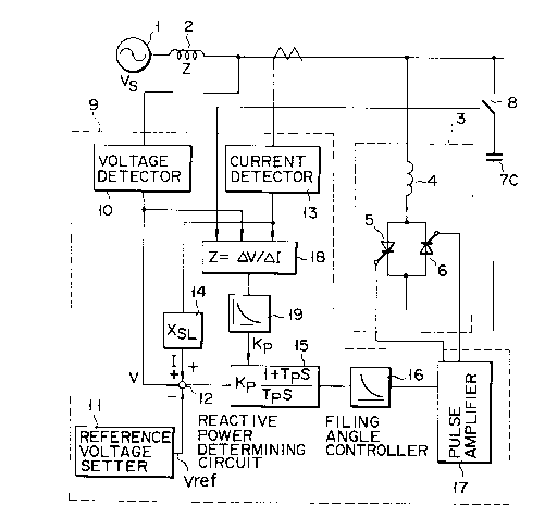
Fig. 1 is a block diagram showing an embodiment of
the present invention.
Referring to Fig. 1, main circuit 3, of the reac-
tive power compensation apparatus, connected to a power
system equivalently represented by AC power source 1
and power source impedance 2 is designed such that an
inverse-parallel circuit consisting of thyristors 5 and
6 is connected in series with reactor 4.
In addition, static capacitor 7C is generally
connected to this power system through switching circuit
8.
Control circuit 9 detects a voltage applied from
the power system as detection value V by using voltage
detector 10. Control circuit 9 then causes difference
detector 12 to detect a difference between detection
value V and reference voltage value Vref set in refer-
ence voltage setter 11. Meanwhile, a current from the
power system is detected by current detector 13 as
detection value I. Detection value I is reduced to
several to a value between 10 and 20% by slope reactance
circuit 14 and is input to difference detector 12.
Difference detector 12 supplies a difference
output, obtained in accordance with two voltage input
signals V and Vref and current input signal I, to
reactive power determining circuit 15 constituted by
an amplifier, a phase compensation circuit, and the
like. Reactive power determining circuit 15 supplies
2Q33 ~67
-- 5
a reactive power signal used for compensation, determined
in accordance with the voltage difference, to firing
angle controller 16 for thyristors 5 and 6, thereby
generating a firing pulse to be applied to thyristors 5
and 6 of main circuit 3, with a phase corresponding to
the reactive power signal. This firing pulse is applied
to the gates of thyristors 5 and 6 through pulse ampli-
fier 17.
In this arrangement, when a voltage drop occurs in
the power system, voltage detector 10 detects system
voltage v, and a difference between voltage v and
reference value Vref is detected by difference detector
12. This difference may be corrected on the basis of
output I from current detector 13. The output signal
from difference detector 12 is amplified by reactive
power determining circuit 15 so as to be formed into a
reactive power signal. Firing angle controller 16 then
outputs a firing pulse with a phase corresponding to
this signal. The firing pulse output is amplified by
pulse amplifier 17 and is used to fire thyristors 5 and
6. Consequently, a delay current flowing in reactor 4
is reduced to suppress a decrease in system voltage.
In contrast to this, if the system voltage is
increased, the phases of firing pulses to be applied to
thyristors 5 and 6 are controlled to increase a current
flowing in reactor 4. With this operation, feedback
control is performed to suppress an increase in system
2~33~57
voltage.
In Fig. 1, upon reception of an ON/OFF switching
signal from capacitor 7C, power source impedance
estimating circuit 18 calculates change ~V in system
voltage V and change ~I in current I, and estimates
power source impedance Z by a calculation of:
z = ~V/~I -- (1)
Gain adjusting circuit 19 adjusts gain Kp of
reactive power determining circuit 15 in inverse
proportion to estimated impedance value Z.
If estimated value Z of the power source impedance
is reduced, since the transient response speed of
control circuit 9 is decreased, gain Kp of reactive
power determining circuit 15 is increased. In contrast
to this, if estimated value Z is increased, since the
transient response speed of control circuit 9 is
increased to cause hunting, gain Kp of reactive power
determining circuit 15 is deceased to stabilize the
system.
Fig. 2 is a block diagram showing another embodiment
of the present invention. Referring to Fig. 3, upon
reception of an ON/OFF switching signal from capacitor
7C, power source impedance estimating circuit 18 esti-
mates power source impedance Z from change ~V in system
voltage V and capacitance C of a static capacitor
according to a calculation of:
z = ~V/~CV ... (2)
2~:33~7
Gain adjusting circuit 19 adjusts gain Kp of
reactive power determining circuit 15 in inverse
proportion to estimated impedance value Z.
If estimated value z of the power source impedance
is reduced, since the transient response speed of
control circuit 9 is decreased, gain Kp of reactive
power determining circuit 15 is increased. In contrast
to this, if estimated value Z is increased, since the
transient response speed of control circuit 9 is
increased to cause hunting, gain Kp of reactive power
determining circuit 15 is decreased to stabilize the
system.
The apparatus shown in Fig. 1 or 2 may be replaced
with a reactive power compensation apparatus (Thyristor
Switched Capacitor: TSC) in which capacitor 7C is turned
on and off by a thyristor switch, and an impedance is
obtained from a system voltage and the capacitance of
the capacitor of the TSC upon turning on or off of the
TSC, thus adjusting the gain in the same manner as in
the above embodiment.
Fig. 3 is a block diagram showing still another
embodiment of the present invention. Referring to
Fig. 3, upon reception of an ON/OFF switching signal
from inductor 7L, power source impedance estimating
circuit 18 estimates power source impedance Z from
change ~V in system voltage V and inductance L of
inductor 7L according to a calculation of:
2033567
Z = ~V-~L/V ... (3)
Gain adjusting circuit 19 adjusts gain Kp of
reactive power determining circuit 15 in inverse
proportion to estimated impedance value Z.
If estimated value Z of the power source impedance
is reduced, since the transient response speed of
control circuit 9 is decreased, gain Kp of reactive
power determining circuit 15 is increased. In contrast
to this, if estimated value Z is increased, since the
transient response speed of control circuit 9 is
increased to cause hunting, gain Kp of reactive power
determining circuit 15 is decreased to stabilize the
system.
Incidentally, power source impedance estimating
circuit 18 can be reduced to practice by a micro-
computer, using a software programmed for aforementioned
equation (1), (2), or (3).
In each embodiment of Figs. 1 to 3, proportional
constant (gain) Kp in the transfer function of reactive
power determining circuit 15 is changed in accordance
with power source impedance z obtained by estimating
circuit 18 (i.e., Kp decreases as z increases). How-
ever, there are alternative methods as follows:
1) time constant Tp in the transfer function of
circuit 15 is changed in response to a change in
impedance Z (Tp increases as Z increases);
2) reactance XsL of slope reactance circuit 14 is
2~33~7
g
changed in response to a change in impedance Z (XsL
increases as Z increases so that detected current
value I decreases);
3) combining above 1) and/or 2) with the embodi-
ment of Fig. 1, etc., so that two more parameters in Kp,Tp, and XsL are changed in response to a change
in impedance z obtained by circuit 18.
Although each control of the above 1), 2), and 3)
can be achieved by a software control using a CPU, these
controls can also be achieved by use of an exclusive
hardware.
As has been described above, according to the
present invention, even if a change in power source
impedance occurs in accordance with a condition in which
the power system is used, since the control system
automatically adjusts its gain, high-speed, stable
control of reactive power can be performed, thus pro-
viding a highly reliable reactive power compensation
apparatus.