Note: Descriptions are shown in the official language in which they were submitted.
2~s~2
l FJ-8209
DIGITAL CROSS CONMECTION APPARATUS
BACKGROUND OF THE INVENTION
1. Field of the Invention : :
The present invention relates to a digital
cross connection apparatus which can be applied to the
cross connection of virtual tributary (VT) signals of ~.
synchronous optical network tSONET) specifications.
: In digital cross connection apparatuses, in
particular broad band digital connection apparatuses,
it is necessary to be able to cross connect VT signals --~
of various VT sizes corresponding to, for example, the
North American 1.5M (Mega bit/second, same below), 3M,
and 6M and CEPT (Conference of European Postal and :~
Telecommunications Administration) 2M signals using a
common hardware construction. Here, the invention will
be explained with reference to primarily VT signals of
the SONET specifications.
~ 2. Description of the Related Art ::
: 20 In a digital cross connection apparatus
handling SONET signals, use is made of VT signals of a : :~
VT format for the frame structure in signal processing ;~
in the apparatus. For example, in the case of cross .
connection of North American 1.5M, 3M, and 6~ signals
use is made, for example, of the VTl.5 size as the
~: cross connection unit and it is possible to
simultaneously cross connect signals of VT3 and VT6
sizes, as these are whole multiples of the VTl.5 size.
CEPT signals, however, have a VT size of`-: ~:
YT2. VT2 is not a whole:multiple of VT1.5, so if it is
: attempted to cross connect VT2 size signals by an
apparatus using VTl.5 as the cross connection unit,
: ~ the efficiency becomes extremely poor. Therefore, :~
cross connection of VT2 had required changing of the
switch units and other hardware so as to handle VT2 :
size cross connection units.
Therefore, in digital cross connection
....... ~ .. .,.. ,. . . . . .. , - :
2 ~ 3 ~
apparatuses handling SONET signals, despite it being
considered necessary to cross connect any signal
input, whether of the CEPT specification or North
American specification, it has not been possible to
make common use of the switch units and other hardware
for these signals, so these signals have not been
handled by the same apparatuses in the past, i.e.,
separate apparatuses have been necessary.
SUMMARY OF THE INVENTION
Therefore, the object of the present invention is
to enable cross connection of any SONET signals, for
example, North American and CEPT SONET signals by
using the same hardware construction.
To achieve the above object, the present
invention provides a digital cross connection
apparatus in which the two or more types of VT signals
are handled in the apparatus after division by common
size units and the thus divided units are used as
cross connection units.
BRIEF DESCRIPTION OF THE DRAWINGS
The above object and features of the present
invention will be more apparent from the following
description of the preferred embodiments with
reference to the accompanying drawings, wherein:
Fig. 1 is a block diagram showing the key
portions of a digital cross connection apparatus to
which the present invention is applied;
; Fig. 2 is a view illustrating the point of the
present invention;
Fig. 3 is a view showing the format of a VT frame
used in the SONET specification;
Fig. 4 is a view showing in further detail the ~`
constitution of Fig. l;
Fig. 5 is a view showing an example of division
of VT signals of VTl.5 size based on the present
invention to obtain divided VT signals;
Fig. 6 is a view showing an example of division
,
.''--'''' .~"
.~.~ ....: .
~ ` 2~ 7~
of VT signals of VT2 size based on the present
invention to obtain divided VT signals;
Fig. 7 is a view showing an example of division
of VT signals of VT3 size based on the present
invention to obtain divided VT signals;
Fig. 8 is a view showing an example of division
of VT signals of VT6 size based on the present
invention to obtain divided VT signals;
Fig. 9 is a view showing the schematic
construction of a divided VT signal serving as a cross
connection unit;
Fig. 10 is a view showing the detailed
construction of a divided VT signal serving as a cross
connection unit;
Fig. 11 is a block diagram showing an example of
a known base construction of an input size interface
unit;
Fig. 12 is a view showing a processing means
according to the present invention which is provided
in an input side interface unit; and
Fig. 13 is a view showing a processing means -
according to the present invention which is provided
in an output side interface unit.
DESCRIPTION OF THE PREFERRED EMBODIMENTS
Embodiments of the present invention will be
described with reference to the drawings.
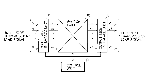
Figure 1 is a block diagram showing the key
portions of a digital cross connection apparatus to
which the present invention is applied. In the figure,
the digital cross conn~ction apparatus includes a
;~ switch unit`10 which pérforms the cross connection, an ;~
input side interface unit 11 which is provided at the
input side of the switch unit 10 and receives a
plurality of input side transmission line signals
composed of two or more types of virtual tributary VT
signals; and an output side~interface unit 12 which is `~
provided at the output side of the switch unit 10 and
` 2~33~72
transmits signals which have been cross connected by
the switch signal as a plurality of output side
transmission line signals. Note that a digital cross
connection apparatus includes a cross connection
control unit 13 compxised of a processor.
The point in the present invention is that the
switch unit 10 is operative to divide the virtual
tributary (VT) sizes of the input side transmission
line signals into whole integers by predetermined
common size units and perform the cross connection
using the resultant divided VT signals as cross
connection units.
In this case, the numbers of bytes of the common
size are selected to be the numbers equal to one of
the common divisors obtained when dividing the number
of bytes of the above VT sizes by whole integers
without reminders.
More particularly, the greatest common divisor
among the common divisors is preferably set as the
number of bytes of the common size.
This will be explained in more detail using
specific examples.
Figure 2 is a view illustrating the point of the
present invention. In the figure, VTl.5, VT3, and VT6
are thxaa types of VT signals based on SONET
specifications, which are mainly of the North American ;
specifications. VT2 is a VT signal based on the SONET
specification, which is mainly of the CEPT
specifications. The VT sizes, in terms of the number ~-
of bytes, are, as illustrated, 108, 144, 216, and 432 `~
bytes. In the present invention, these VT sizes are
divided into whoIe integers by predetermined common
size units and performs the cross connection in the
switch unit 10 using the thus obtained divided VT
signals vt as cross connection units.
Figure 3 is a view showing the format of a VT
frame used in the SONET specification. As shown in the
:' ~ . .
~-` 2~3~72
figure, the VT frame used in the SONET specification
has the format of four VT payload pointer parts V1,
V2, V3, and Y4 and four data parts D of a bytes each.
Here, the VT payload pointer parts Vl, V2, V3, and V4
are each composed of one byte. Further the n~mber of
bytes a of the data parts D is 26 in the case of the
VTl.5 size, 35 in the case of the V2 size, 53 in the
case of the V3 size, and 107 in the case of the VT6
size. Therefore, the total number of bytes is 108 ( 26
x 4 + 4) in the case of the VT1.5 size, 144 (35 x 4 +
4) in tha case of the VT2 sizej 216 (53 x 4 ~ 4) in
the case of the VT3 size, and 432 (107 x 4 + 4) in the ;
case of the VT6 size.
Here, taking note of the VTl.5 size and the VT2 :: :
size, these sizes are not whole multiples of each -
other, so if one of the sizes (VT1.5 or VT2) is used
as the cross connection unit as it is, it becomes
impossible to perform the cross connection commonly
for all these sizes in a common switch unit 10.
According to the present invention, as mentioned
earlier, the most preferable mode is one in which the
greatest common divisor is made the number of bytes of
the common size. In other words, a VT2 size frame is
made up of 4/3 times the number of bytes as a VT1.5
size frame, so the VT2 size is divided by the integer ~;
~;~ 4 and the VTl.5 size is divided by the integer 3 and
36 bytes is used as the unit of cross connection. In
this way, in the digital cross connection apparatus,
common use may be made of the switch unit 10 to cross -
connect the VTl.5 size and the VT2 size.
' Looking at the VT3 size and the VT6 size as well,
these are whole multiples of size of the above cross
connection unit (216 = 36 x 6, 432 = 36 x 12), so it
is similarly possible to perform cross connection
commonly in ~he switch unit 10 using common hardware.
Figure 4 is a view showing in further detail the
constitution of Fig. 1. In the figure, 11#1 to ll#n
'
. ,
7 ~
,.~ ` .
are input side interface units, 10 is the above-
mentioned switch unit, and 12#1 to 12#n are output
side interface units.
The input side interface units 11#1 to ll#n
receive the various types of input side transmission
line signals such as DSl, D';2, DS3, OC-1, and OC-3,
convert these into VT signals for handling in the
cross connection apparatus, divide these into
predetermined cross connection units as mentioned
earlier, use the results as divided VT signals vt, and
transmit them to the switch unit 10. Note that DSl is
a first order group signal, DS2 is a second order
group signal, and OC-1 is an optical carrier (level
1).
- 15 Here, the switch unit 10 is a circuit designed soas to cross connect signals from the input side
interface unit (11) using predetermined cross
connection units. Further, the output side interface
units 12#1 to 12#n function to combine the divided VT
signals which have been cross connected, reconstruct
them, convert them to the original transmission line
signals, and send them to the transmission line as
output side transmission line signals. ~ -~
Below, the operation of the apparatus of this
embodiment will be explained.
The input side interface units 11#1 to ll#n
convert the input transmission line signals to VT
signals of the predetermined VT format and further - ~-
divide the VT signals into whole integers by
predetermined common size. The common size is selected ~ :
so that the VT sizes handled at the input side
interface units 11#1 to ll#n become whole multiples of
each other.
Figure 5 is a view showing an example of division
of VT signals of VTl.5 size based on the present ~-
invention to obtain divided VT signals. In the case of - `~
VT signals of a VTl.5 size, as shown in the figure,
' . '. .:"
",, ~j
`` 2~3~72
VTl.5 frames of 108 bytes are divided into three to
give blocks of 36 bytes each. Additional signals are
attached to each of these (additional bytes) and the
result used as the cross connection unit. This i5 the
divided VT signal vt. The same type of division is
performed for the case of VT2 size, VT3 size, and VT6
size VT signals.
Figure 6 is a view showing an example of division
of VT signals of VT2 size based on the present
invention to obtain divided VT signals. Figure 7 is a
view showing an example of division of VT signals of
VT3 size based on the present invention to obtain
divided VT signals. Figure 8 is a view showing an
example of division of VT signals of VT6 size based on
the present invention to obtain divided VT signals.
Note that in Fig. 6, Fig. 7, and Fig. 8, AD is the
abbreviation for the additional signal of Fig. 5.
Looking at Fig. 6, a VT2 frame made up of 144 ~`
bytes is divided into four and additional bytes are
attached to each block. Similar division is possible
for the VT3 and VT6 sizes using units of 36 bytes as
shown in Fig. 7 and Fig. 8.
Further, since the STS-l signal, a SONET signal
of 50M, is also composed of VT-1.5 x 30 bytes = 4
frames, similar division is possible. STS-l is, as is
well known, a synchronous transport signal-l.
Next, an explanation will be made of the above-
mentioned additional signal.
Figure 9 is a view showing the schematic
construction of a divided VT signal serving as a unit
of cross connection. ~he additional signal is composed
of k (k = l, 2, 3...) bytes as additional bytes and
consists of the frame synchronization information Sf ~:
~` and division number information No. showing the order
of the division in the cross connection apparatus.
More preferably, it includes path identification
information ID showing which one of the plurality of
, ~, ~ ~ . , : :
c, , , ~ j - , i, :
.. -~. , : ,
c ` `~ :
~ ~33~2
cross connection paths ~see the dotted lines in switch
unit 10 in Fig. 4) formed in the switch unit 10 the
divided VT signal vt must pass through. That is, the
frame synchronization information is for frame
synchronization after the cross connection, the
division number information is for showing the order
of the divided VT signals, and the path ID information
is for showing the path route in the switch unit 10.
The common size blocks with these additional
bytes attached are sent from the input side interface
unit 11#1 to ll#n to the switch unit 10. These are
cross connected at the switch unit 10 and sent to the
output side interface units 12#1 to 12#n. The output
side interface units 12~1 to 12#n perform
synchronizations with respect to the input common size
blocks (vt) referring to their additional bytes and -~
reconstruct them to the original VT signals in
accordance with the division numbers No's. They ~;
further convert them into transmission line signals
and output the result. ~
Figure 10 is a view showing the detailed ;
construction of a divided VT signal serving as a cross - ~
connection unit. In the example shown in the figure, j -
the additional signals are composed of 2 bytes, of -
which one byte shows the frame synchronization
information Sf and the other byte shows both ~he path -
ID information and division number information. When
the path ID information becomes "PQ", it shows that ` -~
the divided VT signal is cxoss connected passing
through ~he path between P and Q in the switch unit 10
in Fig. 4. Note that the designation of the path
between P and Q is usually performed by the cross
connection control-unit 13. Further, for example, ~
is written as the division number information, showing
that the divided VT signal is the second divided - -
signal. ~ ~
The portion of the divided VT signal vt remaining ~ ~;
,: ~
~.
?j3~
.
after removal of the additional signal is composed of
the data signals Dl, D2... D36, composed of 36 bytes.
Figure 11 is a block diagram showing an example
of a known base construction of an input size
interface unit. For example, this is the construction
of the unit 11#1 in Fig. 4. The units 11#2 to ll#n
have exactly the same basic construction. Note that
the block of Fig. 11 does nok include the structural
portion of the present invention. Further, the output
side interface units 12#1 to 12#n have the opposite
construction as in Fig. 11 and basically axe the same
as the input side interface in basic construction. -
In Fig. 11, the input side transmission line
signal DSl is first applied to the synchronizing means
(SYNC) 21, where it is synchronized in subordination
to the master clock ~oscillator OSC) in the digital
~- cross connection apparatus. After this, it is applied
to the row/column conversion means (R/C) 22, where the
signal format of the VT signal is converted so as to
facilitate the cross connection in the switch unit 10
mounted at the next stage thereto. Note that the
switch unit 10 usually is of a T-S~T switch
construction, where T means a time switch (T-SW) and S
means a space switch (S-SW).
Figure 12 is a view showing a processing means
according to the present invention which is provided
in an input side interface unit. Figure 13 is a view
showing a processing means according to the present
invention which is provided in an output side
interface unit. However, this shows an example of a
circuit handling a Vl.5 transmission line signal. By
simply changing the division number No., it is
possible to similarly realize a circuit handling VT2,
VT3, ar.d VT6 transmission line signals.
The input side interface unit (11#1) in Fig. 12
has a division means 31 for dividing the input side
transmission line signal (DS1) by an amount
2~ ~3~2
corresponding to the number of the above integers.
The output side interface unit (12) in Fig. 13
has a combining means 41 for combining the plurality
of divided VT signals vt from the switch unit 10 to
reconstruct the VT signal.
In Fig. 12, the division means 31 cooperates with
an additional signal generating means 32 for
generating the additional signals.
In Fig. 13, the combining means 41 cooperates
with a combining controlling means 42 for a combining
control in accordance with the above additional
signal.
In Fig. 13, the combining controlling means 42
further cooperates with a separating means 43 for ` -
separating the additional signals from the
corresponding divided VT signals and inputting the
separated divided VT signals vt' to the combining
means 41. ~-
In Fig. 12, the division means 31 can be realized - -
by the s~ructural elements 311 to 315 shown in the
figure. Reference numeral 311 is a triple-multiplying
circuit which receives timing pulses TP (occurring at
each top of the VT signals in Fig. 5) showing the ~ `~
headers of the frames of the VT signals and multiplies
the frequencies of the same by three. The timing
pulses tp of the triple frequency correspond to the
tops of the blocks ( ~ , ~ , and ~ ) in Fig. 5 At
the timing pulse tp, the switch in the selector (SEL)
312 is successively cyclically switched. This being `
so, the data corresponding to the blocks ~ , ~ , and
` ~ in Fig. 5 is successively cyclically stored in the
memories 313, 314, and 315. -
At the headers of the data successively ` -~
cyclically read out from the memories 313 to 315 are ~ -
given with additional signals. This is done by the
additional signal generating means 32. Specifically,
this means is comprised of an additional signal
..
2 ~ :~ 3 3 7 2
11
generator 321 and OR gate 322. The generator 321
generates at least the frame synchronization
information Sf (Fig. 10) and the division number
information No. (Fig. 10).
The frame synchronization information Sf is
obtained from a pattern generator which produces a
predetermined fixed pulse pattern, e.g., "10101010".
The division number information No. is obtained as the
output of a counter receiving as input the timing
pulse tp, which counter is mounted in the
generator 321.
The path identification inormation (I~) (for
example, PQ in Fig. 10) is in~ormation which naturally
is known by the cross connection control unit 13.
This is used as input for the generator 321.
The above information Sf , No., and ID are attached
to the divided blocks (data parts) at the OR gate 322
to form the divided VT signals vt.
In Fig. 13, the combining means 41 includes a
memory (MEM) 411, a switch 412, and a multiplexer
~MUX) 413. On the other hand, the combining control
means 42 includes the structural elements 421 and 422
shown in the figure. Reference numeral 421 represents
a frame synchronization circuit (SYNC) which monitors
the additional signals in the received divided VT
signals and detects the frame synchronization signals
Sf in the same. By detecting the synchronization
signals Sf, the headers of the frames of the divided VT
signals are recognized.
Using the synchronization signals Sf, the division
number information detection circuit (No.) 422
extracts the bit portion shown by the No. of Fig. 10
and detects the division number ( ~ , ~ , or ~ ).
The division number is input to the switch 412, one
port corresponding to the division number of the
received vt (one of the three ports) is selected, and
the signal from the memory 411 is input through the
~ 2~3~72
12
selected port to the multiplexer 413. A similar
operation is performed for the other division number
signals and the VT signal is reconstructed.
The frame synchronization signal from the frame
synchronization circuit 421 is given to the separation
means 43 as well, where the byte por~ion corresponding
to the additional signal is removed from the divided
VT signals vt and only the data part in the vt is
obtained as vt'. vt' is stored once in the memory ~ ~-
411.
The separation means 43 is comprised mainly of
the gate circuit and passes the signal vt to the
memory 411 side only at every timing where no
additional signal exists, based on the frame
synchronization signal Sf. At other timings, the signal
vt is input to a path identification matching circuit
44. The circuit 44 monitors the ID portion of Fig. 10,
monitoring if the path PQ matches the PQ known from
the cross connection control unit 13, and when not
matching, issues the alarm signal ALM.
As explained above, it is possible to cope with
any SONET signal by just replacing the portions for `;
processing the cross connection units and it is ,
possible to make common use of both the switch unit 10
and other hardware.
Therefore, according to the present invention, it
is possible to cross connect`the North American, CEPT, ~ -
and other specification SONET signals by the same -
hardware.
~
' i ' '"'.. "'`
": :,