Note: Descriptions are shown in the official language in which they were submitted.
2~3~53
COAXIAL TRANSMISSION LINE TO
STRIP LINE COUPLER
Technical Field
This invention relates generally to an electromechanical assembly and
5 more particularly to a connector for coupling a coaxial tr~n~mi~ion line to a strip
tr~nimi~si~n line located on the component side of a printed wiring board.
Back~round of the Invention
In the electronics manufacturing industry, printed wiring boards, also
known as printed circuit boards, are frequently used for mounting large numbers of
10 devices such as hybrid circuits, integrated circuits, individual components and the
like. A printed wiring board normally contains a pattern of conductive traces on the
surfaces of the board; and the board acts as a dielectric material for electrically
coupling the various devices in a desired configuration. Two or more printed wiring
boards can be interconnected through connecting pads, connectors and a backplane.
15 A printed wiring board can comprise either a single dielectric sheet or a plurality of
dielectric sheets l~min~ted together into a more or less rigid l~min~tecl board. The
sheets carry the conductive traces or paths which interconnect the component pads
affixed to the board. Some of the conductive paths connect with connecting pads
which are located on the board at or near an edge of the board for purposes of
20 making connections to circuitry located external to the board. Frequently only one
of the 4 edges is available for such connections. It is desirable to establish such
connection at arbitrary locations throughout the interior of the board.
In data processing systems, the need has arisen to transmit to or receive
from arbitrary locations on a printed wiring board high speed data streams having bit
25 rates which extend into the microwave region, for example, a 2.488 GHz clock
signal and data connections at the electro-optic interfaces of light wave systems. In
these instances the conductive traces are designed to perform as controlled
impedance transmission lines. A controlled impedance transmission line retains the
desired characteristic impedance (for example, 50 ohms) at the interconnection to
30 frequencies extending into the microwave region. Examples of controlled
impedance transmission lines are a strip tr:~nsmi~sion line, a microstrip transmission
line and a coplanar waveguide transmission line.
In one type of assembly, the printed wiring board can include, as the
conductive path, a microstrip transmission line affixed to one side of a dielectric
35 sheet and a relatively wide flat conductor affixed to the opposite side of the dielectric
sheet. A second dielectric sheet is positioned against over the side of the first
203~95~
- 2 -
dielectric sheet having the relatively wide flat con-luctor and a connector for a
coaxial tr~ncmicsion line is coupled to the exposed side of the second dielectric
sheet. It is to be noted that the exposed side of the second dielectric sheet is not
required to support any conductive paths. The coaxial connector is coupled to the
5 conductive paths which can be a trace or strip tr~ncmicsion line located on the far
side of the board assemblage by means of an opening in the board through which
conductive wires can pass. One wire extends through the opening in the dielectric
sheets from the center lead of the coaxial connector to a conductive trace on the far
side of the first dielectric sheet. A second connection is made from the body of the
10 coaxial connector to a conductive pad also located on the far side of the first
dielectric sheet, for coupling the body of the connector to the relatively wide flat
conductor which defines the ground plane located between the two dielectric sheets.
The conductors which pass through the dielectric sheets to connect the
coaxial connector to the strip transmission line and ground plane cause an abrupt
15 change in the physical characteristics of the line which, in turn, cause an abrupt
change in the characteristic impedance of the line. The line, therefore, losses its
controlled impedance performance. This change introduces objectionable electrical
perforrnance and losses to the signal being propagated between the strip transmission
line and the coaxial tr~ncmission line. An improved coaxial trancmission line to20 strip trans-m--ission line coupler is required to reduce this deleterious condition.
Summary of the Invention
In accordance with the principles of the present invention, a coupler for
coupling a coaxial transmission line to a strip tr~ncmission line comprises a length of
coaxial transmission line having an inner conductor having a longitudinal axis, an
25 annular ring of dielectric material disposed around the inner conductor and aconcentric outer conductor. The coaxial transmission line, at one end, is coupled to
a coaxial tr~ncmission line connector. The other end of the transmission line, is
adapted to be mounted to the side of a printed wiring board which supports the strip
tr~nsmicsion line. The very end of the inner conductor, which extends beyond the30 annular ring of dielectric material, is electrically coupled to the strip signal
tr"ncmiccion line on the printed wiring board and the outer conductor is coupledelectrically to the ground plane, which is coupled to the printed wiring board.
2(~33953
- 2a -
In accordance with one aspect of the invention there is provided a
coupler for coupling a coaxial transmission line to a controlled impedance striptransmission line of a type in which a sheet of dielectric material supports a strip
signal conductor on one side and a ground plane on the other, comprising an inner
5 conductor having a longitudinal axis, a first end section and a second end section,
the longitudinal axis of said first end section forming an obtuse angle with thelongitudinal axis of the inner conductor, an annular ring of dielectric materialdisposed around said inner conductor, and an outer conducting member disposed
around said dielectric material, said coupler adapted to be coupled to the strip10 signal conductor side of said sheet of dielectric material intermediate the edges of
said sheet of dielectric material, said first end section of said inner conductor
projects beyond said annular ring of dielectric material and is adapted to be
tangentially aligned with and coupled to said strip signal conductor on said sheet of
dielectric material intermediate the edges of said sheet of dielectric material when
15 said coupler is coupled to the strip signal conductor side of said sheet of dielectric
material, and said outer conducting member is adapted to be coupled to said
ground plane on the sheet of dielectric material.
Detailed Description
In the Drawing:
2~339~3
-
- 3 -
FIG. 1 is a side sectional view representative of a prior art strip
.
tr~n~mi~lon lme-to-coaxlal transltlon;
FM. 2 is a side sectional view of a strip transmission line-to-coaxial
transition in accordance with the principles of the invention;
FIG. 3 is an exploded view of a strip tr~n~mission line-to-coaxial
transition connector in accordance with the principles of the invention;
FIG. 4 is an expanded side view of a coaxial transmission line of the
strip transmission line-to-coaxial transition connector; and,
FIG. 5 is a plot of a portion of a cosine curve which is representative of
10 the shape of the coaxial tr~n~mi~sion line located within the coaxial tr~nsmi~sion
line-to-strip transition coupler.
Referring to FIG. 1, there is illustrated a side sectional view of a printed
circuit or printed wiring board coupled to a coaxial connector for establishing a
propagation path between a strip transmission line and a coaxial cable. A coaxial
15 cable is capable of propagating signals which can extend into the microwave region.
It is to be noted that there is no difference between a strip tr~n~mi~ion line-to-
coaxial transmission line transition and a coaxial tr~n~mi~ion line-to-strip
tran~mi~ion transition, the two being the same.
A printed circuit or printed wiring board 10 can comprise a ground plane
20 12 positioned between a bottom dielectric layer 14 and a top dielectric layer 16.
Strip transmission lines 18, for establishing conductive paths between components,
are mounted on or are a part of the board at discrete locations on the outer surface 20
of the bottom dielectric layer 14.
At a predetermined location on the board 10 a cutout 21 is provided for
25 a coaxial connector 22. The cutout 21 is positioned to be in close proximity to the
portion of the strip transmission line 18 that is to be coupled to a coaxial connector.
The ground plane 12 is coupled to a conductive trace 24 which provide~ a conductive
path from the ground plane 12, to the bottom surface of dielectric layer 14, and the
top surface of dielectric layer surface 16. Conductive trace 24 provides an electrical
30 connection between the ground plane 12 and the housing 28 of the connector 22.
A coaxial connector 22 is positioned on top of the top dielectric layer 16
and resides over the cutout 21 such that the center conductor 27 of the coaxial
connector extends through the cutout 21. In FIG. 1, the coaxial connector 22 can be
a flange mount back receptacle of the type manufactured by M/A-Com Omni
35 Spectra, Inc. of Merrimack, N.H. The coaxial connector contains a flange 28 which
can have four mounting cutouts 30 taped to accept a round head machine screw 34 of
2Q~3~ 3
- 4 -
an applupliate size. The four cutouts 30 in the flange 28 are aligned with four
cutouts 32 located in the board 10. Four machine screws 34, which are positionedwithin the cutouts 32 are threaded into cutouts 30 in flange 28 to rigidly secure the
coaxial connector 22 to the board 10. It is to be noted that the cutouts 32 are
S positioned to avoid interfering with the strip transmission lines 18 located on the
lower surface of the dielectric layer 14 while the ground plane 12 is designed to pass
through the opening 32 to contact the flange 28 both directly and via the mounting
screws 34. It is also to be noted that the coaxial connector is mounted to the side of
the board 10 which does not support the strip tr:~nsmission lines 18.
The center conductor 27 of the connector 22 projects through the
opening 21 and extends beyond the bottom surface of layer 14. To establish a
conductive path, the end of center conductor 27, is bent over to contact the
applopliate strip transmission line 18, and a permanent connection can be made
between the conductor 27 and the conductive trace 18 with solder.
The drastic changes in geometry from the coaxial geometry of connector
22 to the strip transmission line 18 with its ground plane 12 introduces
discontinuities which have a deleterious effect on the propagation of high frequency
energy.
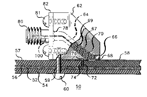
Referring to FIG. 2, there is illustrated a cutaway side view of structure
20 in accordance with the principles of the invention for materially reducing the adverse
effects associated with coupling a strip transmission line to a coaxial transmission
line conductor via a prior art coaxial connector.
As noted above in FIG. 1, a wiring board 50 is comprised of a ground
plane 52 positioned between a bottom dielectric layer 54 and a top dielectric layer
25 56. Conductive traces 58 such as a microstrip, a transmission line, a coplanar
waveguide transmission line pattern or a strip transmission line for establishing
controlled impedance conductive paths between components are supported on the
outer top surface 57 of the top dielectric layer 56.
At predetermined locations on the board 50, clearance cutouts 59 are
30 provided for machine screws 60. The clearance cutouts 59 are positioned to avoid
interfering with the strip transmission lines 58 on the top surface 57 of the top
dielectric layer 56. The ground plane 52 can be recessed from cutouts 59 to prevent
the ground plane from contacting mounting screws 60 or the ground plane can cometo the edge of cutouts 59 to permit the ground plane to contact member 62 via
35 mounting screws 60.
20339~3
- 5 -
Mounting member 62, which can be made of either a conductive
m~t~ri~l, or of a non-conductive m:~teri~l, iS secured rigidly to the top surface of the
top dielectric layer 56 by means of machine screws 60 which pass through clearance
cutouts 58 and thread into member 62. If desired, screws 60 can be replaced by
S mounting pins which can be soldered to the conductive path on the bottom of
dielectric layer 54. Member 62 provides support for coaxial transmission line 64 and
coaxial connector 80. Coaxial tr~n~mi~sion line 64 can be semirigid or flexible and
can be urged to assume a shape which can be characterized as resembling the trace of
a portion of a cosine wave, for example, the trace of the portion of a cosine wave
10 which extends from 0 to 180 as illustrated in FIG. 5.
The outer conducting member 70 and the dielectric insulation 67 at the
bottom end portion 66 of the coaxial tr~n~mi~sion line 64 is removed to expose an
end 68 of the center conductor 69. The lower end 68 of the center conductor 69
projects slightly beyond the end of the dielectric insulation 67 and, when positioned
15 on the printed wiring board, extends over the top surface of the strip tr~nsmi~sion
line 58. Positive contact between the end 68 of the center conductor 69 and the strip
tr~n~mi~sion line 58 can be provided by soldering the two together.
A cutout 72 in the top dielectric layer 56 provides a passage for a
conductor 74 to connect the ground plane 52 to a conductive pad 76 located on the
20 surface 57 of the top dielectric layer 56. Conductive pad 76 can be positioned to
make contact with the outer conducting member 70. If desired, the outer conducting
member 70 can be soldered to conductive pad 76 to provide positive electrical
contact. In those instances where member 62 is composed of a conductive materialsuch as brass, bronze, aluminum, copper or the like, it may be desired to position the
25 conductive pad 76 to be between the member 62 and the top dielectric layer 56, and
soldering may not be required. It is also noted that, where the member 62 is
conductive, it may be desirable to allow member 62 to become the conducting
member 70 and thus the outer conducting member 70 of the coaxial tr~nsmission
line 64 can be eliminated. Obviously, if member 62 is made of a material which is
30 not conducting, and its surface is not treated by plating or the like to be conducting,
then a separate outer conducting member 70 of the coaxial tr~nsmission line is
required.
The upper terminal end 78 of the coaxial tr~n~mission line 64 can be
coupled to a standard bulkhead connector 80 such as model 9954-0081-6220
35 manufactured by Dynawave Incorporated of Georgetown, Mass. Connector 80 can
be secured to a side surface of mounting member 62 by means of machine screws 81.
-6- 2~33953
It is to be noted that the center conductor 100 of connector 80 is a metal tube which
has an inside diameter which fits over the center conductor 69 of the coaxial
tr~nsmission line 64. The outer conductor of the coaxial tr~nsmission line can be
positioned between the mounting member 62 and the flange 82 of the blllkhe~d
S connector to provide a positive electrical connection between the body of the
blllkht a-l connector and the outer conducting member of the coaxial transmission
line.
Referring to FIG. 3, there is illustrated an exploded view of the strip
tr~nsmission line-to-coaxial transmission line connector. In this illustration, the
10 member 62 is composed of brass and the coaxial tr~nsmission line 96 is semirigid, it
being understood, however, that the member 62 can be comprised of other materialand that the coaxial transmission line 96 can be flexible and, where the member 62 is
conductive, the outer conductor of the coaxial transmission line can be elimin~ted.
It is also to be understood that conductive trace or line 91 can be in the
15 form of a microstrip transmission line, a coplanar waveguide type of transmission
line or a strip tr~nsmission line geometry. In this embodiment, the mounting
member 62 can be formed of two members, a lower member 90 and an upper
member 92. The lower member 90 supports a slot 94 which accommodates, in this
embodiment, a semirigid coaxial transmission line 96 bent into a partial cosine type
20 of shape as illustrated in FIG. 5. The coaxial tr~nsmission line 96, which is more
clearly illustrated in FIG. 4, fits into slot 94. The upper member 92 fits on top of the
lower member and contains a slot 97 which is sized to accept the upper portion of
the coaxial tr~nsmission line. Machine screws 98, which pass through the upper
member and are threaded into the lower member, lock the lower member to the
25 upper member and hold the coaxial transmission line captive. The center sleeve
conductor 100 of the bulkhead connector 101 is slidably coupled to the projecting
center end 102 of the coaxial transmission line 96 and the connector is then coupled
to the upper and lower members 90 and 92 by means of machine screws. Machine
screws, which can pass through clearance openings in a printed wiring board are
30 threaded into the assembled member 62 to lock it to a printed wiring board.
It is to be noted that the connector here disclosed is mounted on the side
of a printed wiring board which supports the strip transmission lines. This is exactly
the opposite of the prior art connectors which are not mounted on the side of the
printed wiring board which supports the strip transmission lines. In this invention,
35 prior to assembly, a portion of the lower end of the outer conductor and a portion of
the dielectric insulator of the coaxial transmission line is removed to expose the
2QCJ39~93
- 7 -
center conductor (104), see FIG. 4. The coaxial tr~n~mi~ion line 96 is positioned
within the groove 94 of the lower member 90, and member 90 is mounted onto the
printed wiring board by means of the mounting screws. The exposed end of the
center conductor, which extends slightly past the end of the outer conductor, lies on
5 top of the associated strip tr~nsmi~sion line and can be soldered to the striptr~n~mission line to provide a positive electrical path. The outer conductor of the
coaxial transmission line 96 can be soldered to a pad located on the top surface of
the printed wiring board and coupled to the ground plane. The impedance of the
strip tr~n~mi~ion line can be designed to match that of the coaxial tr~n~mission line,
10 typically 50 ohms, to provide optimum transmission conditions. Next the uppermember 92 of mounting member 62 is assembled over the lower member 90 to lock
the coaxial transmission line in position, and, to provide a protective cover over the
connections. Both the upper and lower member provide mounting holes for the
bulkhead connector. The center conductor 100 of the bulkhead connector is then
15 slidably coupled to the protruding center conductor 102 of the coaxial tr~n~mi~sion
line 96 and the connector 101 is secured to the member 62 by means of machine
screws.
In the embodiment disclosed above, the coaxial transmission line-to-
strip line coupler is illustrated with a printed wiring board having a strip
20 transmission line on one side of a dielectric board and a ground plane on the obverse
side of the dielectric board. In those instances where the conductive paths or traces
on the printed wiring board are of a coplanar waveguide type of transmission line,
the strip signal conductor and the ground plane conductor are both on a common
surface of the dielectric sheet and are separated by a fixed gap. The conductive25 traces, both of which are on the same side of the dielectric board are routed to
contact its ~p~ liate part of the coupler. Thus, the conductive trace coupled to the
signal is positioned to contact the center conductor 68 of the coupler and, the
conductive trace coupled to ground is positioned to contact the outer conductingmember 70 or the member 62, whichever is ~plopliate.