Note: Descriptions are shown in the official language in which they were submitted.
2 0 3 ~ 1 5 3 FJ,FEC-8267
DIELECTRIC FILTER WITH ATTENUATION POLES
1. Field of the Invention
The present invention relates to a dielectric
filter which is provided with attenuation poles to
improve its passband characteristics.
2. Description of the Related Art
A ~/4 resonance coaxial type filter comprising
a plurality of coaxial resonance conductors which are
successively coupled with each other, is used as a
microwave bandpass filter.
This type of dielectric filter has
shortcomings in that the manufacturing process therefor
is complex and an improvement in frequency accuracy is
not easy because the frequency accuracy is dominantly
determined by dimensional accuracy of a dielectric
block, such as ceramics.
A so-called tri-plate type dielectric filter
has been proposed to overcome the above shortcomings.
In the tri-plate type dielectric filter, a plurality of
resonance conductors are combined into a conductor
pattern having a plurality of resonance elements. The
conductor pattern is interposed between two dielectric
plates, outside which metallization is applied.
Also, a dielectric filter, wherein a conductor
pattern having a plurality of resonance elements is
formed on one surface of a dielectric block and the
other surfaces of the dielectric block are metallized,
has been proposed. This filter corresponds to one of
two fragments formed by cutting the tri-plate type
dielectric filter along its plane of symmetry.
It is known to form attenuation poles in the
frequency characteristic curve of a filter having
successively coupled resonance elements, in order to
sharpen the curve or to eliminate specific frequency
components such as a leakage of a local oscillation
frequency.
2034 1 53
-- 2
The poles are formed by providing a bypass in
which phase and amplitude of a signal are varied, so that
the junction phase difference for the specific frequency
becomes 180 and attenuation factors for the specific
frequency are identical.
For the former tri-plate type dielectric filter,
forming of the attenuation poles is not known. For the
latter type filter, attenuation poles can be formed by
coupling two resonance elements through a coaxial cable
having a specific length.
This construction makes the filter size large
because a pattern for connecting the cables is required,
and this makes the size of a casing for the filter large
because space for the cable is required, as described in
Japanese Unexamined Patent Publication (Kokai) No. 58-
166803.
A dielectric filter with attenuation poles,
wherein the above shortcomings are overcome, is disclosed
in the above publication. The filter comprises two
dielectric filter plates fixed to each other back to back.
Two holes are provided for coupling between the resonance
elements on the different dielectric filter plates. One of
the two holes provides part of a main transmission path and
the other hole provides the bypass.
This structure makes the dielectric filter unit
compact, but the range where phase shift and bypass
attenuation factor can be varied is so narrow that the
position and height of the poles cannot be freely designed,
and adjustment of the poles after assembly is not easy.
SUMMARY OF THE INVENTION
It is a feature of one embodiment of the present
invention to provide a compact dielectric filter with
attenuation poles, wherein the position and intensity of
the attenuation poles can be freely designed and easily
adjusted after assembly.
203 4 1 53
-- 3
In accordance with an embodiment of the present
invention there is provided a dielectric filter with
attenuation poles comprising: first dielectric means having
surfaces; a conductor coating partially covering the
surfaces of said first dielectric means; a first conductor
pattern on a portion of said first dielectric means which
is not covered by said conductor coating, said first
conductor pattern having a plurality of projecting portions
which provide a plurality of resonance elements, said first
conductor pattern cooperating with said first dielectric
means and said conductor coating to form a dielectric
resonator having a plurality of stages; second dielectric
means; and a second conductor pattern formed on said second
dielectric means and coupled with at least two of said
plurality of resonance elements.
In accordance with another embodiment of the
present invention there is provided a dielectric filter
comprising: a first volume of dielectric material having a
plurality of surfaces, at least one of said plurality of
surfaces being an indented surface; a first conductor
pattern adjacent at least one of said plurality of
surfaces, said first conductor pattern including resonance
portions; a conductor coating on at least portions of the
plurality of surfaces of said first dielectric volume, said
first conductor pattern, said first volume of dielectric
material and said conductor coating forming a dielectric
resonator; a second volume of dielectric material in said
indented surface of said first volume of dielectric
material; and a second conductor pattern on said second
volume of dielectric material and coupled to at least two
of said plurality of resonance portions of said first
conductor pattern.
In accordance with yet another embodiment of the
_ 4 _ 20341~3
present invention there is provided a bandpass filter,
comprising: a dielectric filter having first and second
resonance elements, said dielectric filter including a
first volume of dielectric material having an indented
surface; a second volume of dielectric material in said
indented surface of said first volume of dielectric
material, said second volume of dielectric having a
surface; and a conductor pattern on said surface of said
second volume of dielectric material, said conductor
pattern being coupled to said first and second resonance
elements of said dielectric filter.
BRIEF DESCRIPTION OF THE DRAWINGS
Figure 1 is a partially cutaway perspective view
of a tri-plate type dielectric filter;
Figure 2 is a perspective view of a dielectric
filter with attenuation poles derived from the dielectric
filter shown in Fig. 1, according to the first embodiment
of the present invention;
Figure 3 is a perspective view of one of the
dielectric blocks of the dielectric filter shown in Fig. 2;
Figure 4 is a cross-sectional view of dielectric
blocks for explaining additional merits of the dielectric
filter shown in Fig. 2;
Figure 5 is a perspective view of another prior
dielectric filter;
Figure 6 is a perspective view of a dielectric
filter with attenuation poles derived from the dielectric
filter shown in Fig. 5, according to the second embodiment
of the present invention;
Figure 7 is a perspective view of a dielectric
block of the dielectric filter shown in Fig. 6; and
Figures 8A to 8G are plane views of various
bypass patterns, according to the present invention.
DESCRIPTION OF THE PREFERRED EMBODIMENT
Figure 1 shows a structure of the aforementioned
2034 1 53
-- 5
tri-plate type dielectric filter. A conductor pattern 3
has four resonance elements 4, to 44, and the conductor
pattern 3 is interposed between two dielectric blocks 1.
Conductor metallization 2 (denoted by hatching) is applied
on the outer surfaces of the dielectric blocks 1.
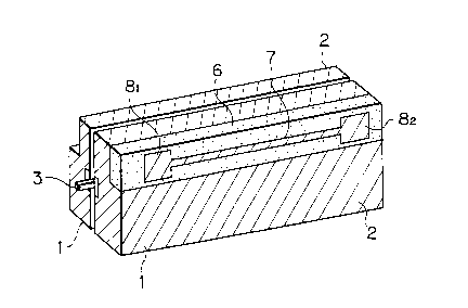
Figure 2 shows a tri-plate type dielectric filter
with attenuation poles which is derived from the dielectric
filter shown in Fig. 1, according to the first embodiment
of the present invention. A conductor pattern 3 has four
resonance elements 4, to 44 (not shown; cf. Fig. 1) between
two dielectric blocks 1. The dielectric blocks 1 are cut
out along upper edges, and one of the cut out spaces is
filled with another dielectric block 6. A conductor
pattern 7 to provide a bypass is formed on the dielectric
block 6. The conductor pattern 7 has two pads 81 and 82 on
both of its ends. The pads 81 and 8z are capacitively
coupled with the resonance elements 4, and 44 (cf. Fig. 1),
respectively.
Figure 3 shows one of the dielectric blocks 1,
which engages with the dielectric block 6. Conductor
metallization is also applied on the surface of the cut out
portion, except for circular portions 9 between resonance
elements 4, and 44 and pads 81 and 82 which are coupled with
each other. The circular portions 9 enable capacitive
coupling between the resonance elements 4, and 42 and pads
81 and 82, respectively to provide the bypass.
Figure 4 is a cross-sectional view of the
dielectric filter shown in Fig. 2, except the dielectric
block 6, to explain additional merit derived from its
shape.
As the dielectric blocks 1 are cut out in an
upper portion, the distances between the upper portions of
the resonance elements 4, to 44 and conductor coatings 2
become short, so that load capacities are formed therein.
The load capacities lower resonance frequencies of the
2034 1 53
- 5a -
resonance elements. As a result, the height of the filter
(I1 + l2) can be lowered.
Additionally, as a difference in thickness is
formed, coaxial impedance is divided into Z1 and Z2l SO that
an effect in which harmonic frequencies are shifted, is
obtained.
Figure 5 shows a structure of the aforementioned
second type of dielectric filter wherein a conductor
pattern 3 is formed on one surface of a dielectric block l
and the other surfaces are metallized (2). The conductor
pattern 3 has four resonance elements 41 to 44 and three
strips 51 to 53 which reach the upper surface. The strips
51 to 53 are provided to vary coupling intensity between
neighbouring resonance elements.
Figure 6 shows a dielectric filter derived from
the dielectric filter shown in Fig. 5, according to the
second embodiment of the present invention.
A dielectric block l is cut out along upper
edges, and the cut out space is filled with another
dielectric block 6. A conductor pattern 7 is formed on the
dielectric block 6 to provide a bypass. The conductor
pattern 7 has two pads 81 and 82 on both of its ends. The
pads 81 and 82 are capacitively coupled with the resonance
elements 41 and 44, respectively.
Figure 7 shows the dielectric block l shown in
Fig. 6. A folded or stepped pattern 3 is formed on a
folded surface of the dielectric block l, and conductor
metallization is applied on the other surfaces of the
dielectric block l.
Though in the example shown in Fig. 6, a cut out
portion is formed on the pattern side, the cut out portion
may be formed on the opposite side. In this case two holes
to enable capacitive coupling must be formed, as shown in
Fig. 3.
Figures 8A to 8G show various bypass patterns for
2034153
use in the dielectric filter with attenuation poles
shown in Figs. 2 and 6.
A bypass pattern shown in Fig. 8B comprises a
capacitively coupled portion 10. Intensity of the
coupling in portion 10 mainly affects the bypass
attenuation factor. Therefore, the bypass attenuation
factor can be designed by adequately determining a shape
of the portion 10, and can be adjusted by altering the
shape after assembly.
A bypass pattern shown in Fig. 8C comprises a
plurality of capacitively coupled portions 12, 14, 16,
and 18.
A bypass pattern shown in Fig. 8D comprises a bent
portion 20. As the length of the bent portion 20 mainly
affects the quantity of phase shift in the bypass, the
quantity of the phase shift can be designed by
adequately determining the length of the bent portion
20.
A bypass pattern shown in Fig. 8E comprises two
open stubs 22, 24 separated from each other by ~g/4. As
the effective length of the bypass depends on the length
of the open stubs 22, 24, the amount of the phase shift
can be designed by adequately determining the length of
the open stubs 22, 24, and can be adjusted by altering
the length of the open stubs 22, 24 after assembly.
In Fig. 8F, a dielectric plate 26 is put on the
bypass pattern, in order to increase an effective
dielectric constant around the bypass pattern. The
quantity of the phase shift can be altered by altering
an area of the dielectric plate 26.
In Fig. 8G, a tapered dielectric plate 28 is put on
the bypass pattern. The effective dielectric constant
around the bypass pattern can be altered by moving the
dielectric plate 28 up or down.