Note: Descriptions are shown in the official language in which they were submitted.
- 1 2~3~9
A system for Controlling
an Internally-Installed Cache Memory
1'he present invention relates to a system for
controlling an internally-installed cache memory to
s mclintain consistency between a main memory and a~.
internally-installed cache in a data processin~
apparatus and for internally-installing the cache into
wl)ich the data in the main memory is copied.
To laeet recent demand for a high-speed data-
processing apparatus, the data access to the mainmemory must be speeded up. Therefore, a cache memory
for co~ying data from the main memory is provided in
tl1e data processing apparatus and the cache is made
1arger.
To raise the performance of the apparatus,
increased use has been made of a multi-processor
sl-ructllre with a plurality of micro-processors (MPUs)
instead of a single micro-processor, and of a system
in which a DMA controller is used to speed up
translaission speed between memories.
Wl~ere a system with such a structure has a cache
memory installed in an MPU/CpU, it is nonsense that
data of the main memory in which the content has
a1ready been changed because another processor has
written data in the main memory is maintained in the
203~7Q9
internally-installed cache memory. Thus, it is
necessary to maintain consistency between the
internally-installed cache memory and the main memory.
To ~aintain consistency between the internally-
installed cache memory and the main memory, a functioncalled an address monitor is conventionally used.
This address monitor observes the system bus to which
the main memory is connected. When the other bus
master produces a write signal for the main memory,
the address monitor reads the address on the system
bus and compares it with the content in the tag
portion of the internally-installed cache memory.
When the address accords with the content in the tag
portion, the corresponding data in the internally-
installed cache memory is invalidated. Thus,consistency is maintained between the main ~emor~ and
tlle internally-installed cache rnemory.
As an ordinary program is written using a logic
address, it is necessary to translate the logic
acldress to a physical address so that the program can
~ operated on an actual hardware. This operation is
called an address translation.
The offset portion of the logical address
sllbjected to this address translation is not changed
iil the physical address and the portion other than the
2~3~709
- 3 -
orfset portion is not the same as that of the physical
a~dress when the logical address is translated to the
physical. address according to the address translation
table.
As the internally-installed cache is small in the
c)nvel1tional data processing apparatus, only the
offset portion of the logical address is used as a set
address, thereby forming an N-way set associative
cache. In this case, the offset portions of the
logical address and the physical address are the same,
even if they are subjected to address translation.
lherefore, the physical address output on the system
bus is directly used to determine a set address of the
clche co be subjected to a comparison and to access
the set address of the cache in which the content
corresponding to the physical address is stored.
Where, in accordance with a request for a larger
cache memory, the cache is made larger, the offset
r)ortion is insufficient for the set address. A bi.t
~ositl.on for which the logical address may be
different from the physical address is used.
Wl~en the physical address of the system bus is
used as the set address of the cache, there is no
problem when the logical address is the same as tle
physi.cal address. When the logical address is
203~7~9
-- 4
dif~erent from the physical address, the conventional
control invalidates a different content of the cache
memory and the portion of the cache memory which
shoul.d be invalidated remains valid.
Views showing the state of the cache, shown in
Ligures lA, lB and lC. are explained. In the
following explanation, LA represents a logical address
and PA represents a physical address. LA(a:b)
represents a bit series from the a--th bit to the b-th
hi.t of the logical address. PA(a:b) represents a bit
series from the a-th bit to the b-th bit of the
phys~cal address. In this example, both the logical
address and the physical address comprise 32 bits.
rl'he highest bit is the 31st bit and the lowest bit is
0th bit.
Tlle address translation table shown in Figure 1A
is provided and correspondence between the address and
the data is as shown in Figure 1B. The data is
rcgi.stered in the cache as shown in Figure 1C in which
the tag portion and the cache memory portion are
shown.
When PA(31:0) = H'00003000 is provided on a
systeM bus as an address to be address-monitored, and
~A~14:4) = H'300 is a set address, PA(31:12~ = H'0003
on the system bu~ is compared with H'0002 stored i.n
293~7~9
-- 5 --
the set address H'300 in the tag portion and as they
do not coincide, the data stored in the set address
ll'300 is not subjected to any operation. PA(31:0) =
ll'00003000, which should be originally invalidated,
remains.
When the portion of the logical address other
than the offset portion is used as the set address of
the cache, the physical address cannot determine the
set address to be subjected to the address comparison.
Tllerefore, where the portion of the logical
address other than the offset portion is used as the
set address of the cache of the set associative
structure, the conventional method cannot maintain
consistency between the main memory and the
internally-installed cache.
Summary of the Invention
An object of the present invention is to maintain
consistency between a main memory and an internally-
il~sta]1ed cache even when the portion of the logical
address other than the offset portion is used as tl1e
set address of the cache.
A feature of the present invention resides in a
cache memory control system in a computer system
comprtsing a main memory apparhtus, a plurality of
data processing apparatuses with respective CPUs and a
CA 02034709 1997-11-06
system bus connecting them. The cache memory control system
comprises a cache memory portion and a tag portion. They are
provided in sald CPU and have an N-way set associative
structure. The cache uses A blts of an offset portlon which
is not sub~ected to the address translation of the loglcal
address and a B-blt portion other than the offset portion.
The B-bit portion is subiected to an address translation. The
cache also uses an address monltor portlon having a tag
portion corresponding to the tag portion of the CPU uslng only
A bits of the offset portion of the set address which are used
as the set address ln said CPU and having 2B x N-way set
associative structure and means for making the tag portion of
the CPU correspond to the tag portion of the address monltor
portion. Thus, it manages the N address stored in said tag
portion and transmits the result of the address observation to
the CPU and invalidates the corresponding recording portion of
the tag in the CPU.
In accordance with the present invention there is
provided a cache memory control system for use in a computer
system including a main memory apparatus; a plurality of data
processing apparatuses with respective CPUs, said respective
CPUs receiving data on a data bus and logical addresses on an
address bus, and said respective CPUs performing address
translation of the logical addresses which are received so as
to translate the logical address to a physical address; and a
system bus connecting said data processing apparatuses and
said main memory; said cache memory control system comprising:
a cache memory portion and a tag portion, which are provided
28151-26
CA 02034709 1997-11-06
- 6a -
ln each of the said respectlve CPUs, said tag portlon
recelvlng a logical address havlng A blts ln an offset portion
and B blts ln a portion other than sald offset portlon, said
cache memory portlon having A bits of sald offset portlon of
said loglcal address, and sald B blts of sald portlon other
than said A bits of sald offset portion; said A blts not being
subjected to an address translatlon of sald loglcal address,
and sald B blts belng subjected to an address translatlon
whereln, when the cache memory portlon and tag portlon ls
accessed by the logical address, the cache memory portion and
tag portlon ls accessed by sald A blts of the offset portlon
of the loglcal address, and said B bits in other portion than
the offset portion of sald loglcal address; and an address
monltor portlon havlng a tag portlon, said address monltor
portlon storlng physlcal address lnformatlon stored ln sald
tag portlon provided ln the CPU at a reglon correspondlng to
sald B bits of the logical address and uslng only sald A blts
of the offset portlon of a set address which is used as the
set address ln said CPU and havlng a 2B x N-way set
assoclatlve structure, and sald address monitor portion having
means for causlng an address stored in said tag portlon
provlded ln said CPU correspond to the correspondlng address
stored ln sald tag portlon of sald address monltor portion,
whereln, when the cache memory portlon and the tag portion are
accessed by the physlcal address, the address monltor portlon
ls accessed by the A blts of the physlcal address transmltted
through an external bus, a part of the physlcal address ls
compared wlth the physlcal address lnformatlon stored in the
28151-26
CA 02034709 1997-11-06
- 6b -
address monitor portlon by using the A blts of the physlcal
address, a posltlon lnformatlon of the region at which the
part of the physical address accords with the physical address
lnformation stored ln the address monitor portlon ln which
each physlcal address informatlon ls stored ln each of 2B x N
reglons and ls selected by uslng sald A blts as a set address
ls encoded to provlde the B blts, thereby lnvalldatlng the
cache memory portlon and lts tag portlon by uslng sald logical
address which is composed of said A bits and said B bits, so
that, when another CPU updates the contents of the physlcal
address, the correspondlng contents of sald cache memory
portlon ls lnvalidated.
In accordance with the present inventlon there is
also provlded a cache memory control system lnternally
lnstalled ln a CPU, comprlslng: a flrst memory to be accessed
by an address havlng A blts concatenated wlth B blts; a second
memory to be accessed by an address havlng A blts and said
second memory comprlslng 2B reglons ln an address deslgnated
by A blts; means for writing informatlon lnto said address of
sald flrst memory designated by said A bits concatenated with
B blts and for wrlting said informatlon into one of 2B regions
corresponding to a binary code of B bits ln said address
deslgnated by sald A blts in sald second memory durlng a
reglstratlon operatlon; comparlson means for, when external
lnformation including said A bits and said information is
provided, and said second memory ls accessed by uslng A blts
of sald external lnformation, readlng the content of sald
address deslgnated by A blts and comparlng the content of
28151-26
CA 02034709 l997-ll-06
- 6C -
respective 2B regions which are read out with said information
of said external information, and detecting a region ln whlch
- the read-out information accords with said information of said
external information; converting means for convertlng through
an encodlng operation a position information of one of the
regions 2B at which the read out information accords with said
information of said external information; and invalidating
means for comblnlng sald B blts wlth sald A bits to provlde A
bits concatenated with B bits, thereby accessing said first
memory and invalidating the content of the accessed address of
said first memory by using said A bits concatenated wlth B
bits.
In accordance with the present invention there is
also provided a cache memory control system, comprising a
memory to be accessed by a physical address on an external
address bus, said physical address being composed of A bits
concatenated with B bits, said A bits comprising an offset
portion of said physical address on the external address bus;
an address monitor portion to be accessed by said A bits;
comparing means for reading a physical address from said
address monitor portion by using said A bits of said offset
portion of said physical address on said external address bus,
for comparing the physical address read from the address
monitor portlon wlth the physical address carried on the
external address bus, to select a position information
corresponding to one of 2B reglons; conversion means for
encodlng the position information obtained as a result of the
comparisons to produce converted information comprising B
28151-26
CA 02034709 1997-11-06
- 6d -
blts; and lnvalldatlon control means for formlng sald A blts
concatenated wlth B blts by using B bits from the converted
lnformatlon produced by the converslon means and A bits of an
offset portion of physlcal address carrled by the external
address bus, said lnvalldatlon control means supplylng an
address havlng A blts concatenated wlth B blts to a tag
portion of a cache, and sald lnvalidatlon control means
causing a valid lnformation stored in the memory to become
lnactive ln order to invalidate the content of said memory
correspondlng to the address provlded by A bits concatenated
with B bits which are supplied by said invalidation control
means.
In accordance with the present invention there is
also provided a memory control system comprlslng: a flrst
memory to be accessed by a loglcal address including A bits
concatenated with B bits; a second memory whlch is accessed by
another address, said another address being composed of A
bits, and wherein sald second memory comprlses 2B reglons ln
sald another address deslgnated by A blts; means for wrlting a
part of a physical address into an address of said flrst
memory deslgnated by A blts concatenated with B bits and
wrltlng the same physical address as written in the first
memory ln at least one of sald 2B reglons in said address
designated by A blts ln the second memory during a
reglstratlon operatlon; comparlson means for, when external
lnformatlon lncluding sald A blts and blts representing the
physical address is provlded to the second memory, accesslng
the second memory by uslng A blts of the external information,
28151-26
CA 02034709 1997-11-06
- 6e -
readlng the content of sald address deslgnated by A blts and
comparlng the content of the respectlve 2B reglons wlth sald
part of the physlcal address of sald external lnformatlon, and
detectlng the reglon ln whlch the part of the physlcal address
stored ln the reglon accords wlth the part of the physlcal
address of the external lnformatlon durlng an address monltor
operatlon; and lnvalldatlng means for produclng B blts by
encodlng the result of sald comparing means, comblnlng the B
blts wlth the A blts to provlde A blts concatenated wlth B
blts, thereby accesslng sald flrst memory and lnvalldatlng
lnformatlon stored ln sald flrst memory by uslng A blts
concatenated wlth B blts when an external CPU changes the
content ln a maln memory whlch corresponds to the physlcal
address.
In accordance wlth the present lnventlon there is
also provlded a memory control system comprlslng~ a flrst
memory to be accessed by A blts concatenated wlth B blts, and
whereln sald flrst memory has lnformatlon wrltten thereln; and
an address monltor means comprlslng: a second memory for
storlng sald lnformatlon ln one of 2B reglons of an address of
sald second memory, sald reglon belng determlned by
lnformatlon correspondlng to sald B blts and sald address
belng accessed by sald A blts and means for reproduclng sald B
blts based on reglon ln whlch external lnformatlon colncldes
wlth sald lnformatlon ln sald second memory, thereby produclng
A blts concatenated wlth B blts ln sald flrst memory.
28151-26
CA 02034709 1997-11-06
- 6f -
Brlef DescriPtlon of the Drawlnas
Figures lA to lC show vlews of a state explanatlon
of the cache to explaln the problem to be solved by the
present lnventlon,
Flgures 2A and 2B show examples of a structure of the
present lnventlon,
28151-26
203~7a9
-- 7
l~'igures 3A and 3B show explanatory views of the
correspondence between a CPU and an address monitor
portion in the preferred embodiment of the present
invention,
Figure 4 shows an example of a data registration
to a cache according to the preferred embodiment of
the present invention,
Figure 5 shows an example of an address monitor
according to the preferred embodiment of the present
i nvention,
Figures 6A to 6D show circuit diagrams of the
blocks shown in Figures 4 and 5,
Fig~re 7 shows a block diagram for explaining the
relation between a TLB and cache according to the
prefer-red embodiment of the present invention, and
Figure 8 designates a timing chart of a read
operation in the block diagram in Figure 7.
Description of the Preferred Embodiment
Figures 2A and 2B show the preferred embodiment
of the present invention.
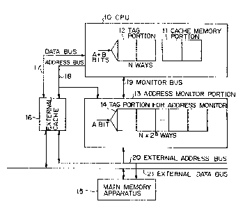
In Figure 2A, CPU 10 performs an arithmetic
o~eration and a memory manaqement, for example. The
cPu 1 n contains a cache memory portion 11 and a tag
portion 12 of the cache memory portion 11. An address
monitor portion 13 is provided to the internally-
~3~a9
-- 8 --
installed cache and a tag portion 14 to the addressmol1i.tor portion 13 corresponding to the tag portion 12
of the CPU 10. A main memory apparatus 15 stores a
program or data processed by the CPU 10. An external
cache l6 is provided to decrease the load of the
system bus. It has a larger capacity than the cache
i.nstalled in the CPU 10. A data bus 17 and an address
hlls 1~ are connected to the CPU 10. A monitor bus 19
is connected between the CPU 10 and the address
monitor portion 13. The data bus 17 and the address
bus 18 are connected to an external data bus 21 and an
external address bus 20, respectively, through the
external cache 16,
The present system comprises a plurality of data
proces~ing apparatuses, a main memory apparatus 15,
and a system bus comprising an external address bus 20
and an external data bus 21 which connect a plurality
o~ data processing apparatuses and the main memory
apparatus 15.
Al: I,east one of the data processing apparatuses
comprises the CPU 10, the address monitor portion 13
and the external cache 16. The data bus 17 connects
the CPU 10 and the external cache 16, and the address
h~ls 18 connects the CPU 10 to the external cache 16
and the address monitor portion 13. The external
2~3~70~
g
address bus 20 connects the main memory apparatus 15
to the address monitor portion 13 and the external
cache 16. The external data bus 21 connects the main
memory apparatus 15 to the external cache 16.
In this embodiment, the CPU 10 and the address
monitor portion 13 are formed of different chips. The
CPU 10 performs an address translation from logical
address I.A to physical address PA by using the portion
o~-her than the offset portion as an ob~ect of the
address translation, as shown in Figure lB.
The cache memory portion 11 and the tag portion
1 ;~ in the CPU 10 use A bits in the offset portion of
the ]ogical address and B bits in the portion other
than the of fset portion as shown in Figure 1 B. The
cache is accessed by using a set address of (A+B)bits,
therehy forming an N-way set associative structuIe.
The tag portion 12 has an address information
recording portion for updating the address of the data
stored in the cache memory porti on 1 1 in the mai n
memory apparatus 1 5 and a recording portion
desiqnating that the data of the cache memory portion
11 is effective.
The address monitor portion 13 is used for
maintaining the consistency of the content of the
cache memory portion 11 in the CPU 10 and the main
2~347~
- 10 -
memory apparatus 15. The address monitor portion 13
contains the address monitor tag portion 14, which
uses only A bits of the offset portion of the set
address used in the CPU 10 for accessing the tag
portion 12 of the cache as the set address of the
address monitor tag portion 14 and has 2B x N-way set
associative structures. That is, 2B x N regions (WAY0
to WAY15) exist in the address monitor tag portion 14,
which is accessed by the set address (equal to A bits
of the offset portion). When a set address is
provided to the address monitor tag portion 14, a
physical address is read out from a particular one
~for example, W~Y2) of 16 regions. This particular
region is designated by B~log N when the physical
address is written in the address monitor 13. In this
embodiment, as the number N of the way is 2, and B
comprises 3 bits, for example, B~log N=4 bits and one
of 16 ways is selected as described in detail later by
referring to Figures 4 and 5.
In this data processing apparatus, the tag
portion 12 of the CPU 10 is made to correspond to the
address monitor tag portion 14 of the address monitor
portion 13. The chip of the address monitor portion
13 performs an address monitor function, thereby
sending the result of the monitoring function to the
~03~70~
CPU 10, and then invalidating the corresponding
recording portion of the tag portion 12 in the CPU 10.
In the present embodiment, when the address
monitoring is performed as shown in Figure 2A, the
pl-ysi.cal address of the external address bus 20 is
compared with the content of 2B x N ways of the
address monitor tag portion 14 for a set address of A
bits. The result of the comparison of the respective
ways (~B x N ways) is converted to B bits of the set
address of tag portion 12 in the CP~ 10, a way signal
and an invalidation enable signal designating whether
the invalidation is performed and then is transmitted
to the C~U 10.
The CPU 10 combines B bits with A bits of the
offset portion of the physical address on the external
address bus 20 which i.s transmitted through the
monitor bus 19 and determines the corresponding
address set of the tag portion 12 in the CPU 10 and
invalidates a valid bit of the corresponding portion
L,ased on the way signal output from the address
monitor portion 13, thereby maintaining consistency
between the main memory apparatus 15 and the
interna3ly-installed cache in the CPU 10.
~'igures 3A and 3B show the correspondence
relation between the CPU and the address monitor
203~7~9
portion in the preferred embodiment of the present
invention, Figure 4 shows an example of the data
registration into the cache in the preferred
embodiment of the present invention, Figure 5 shows an
example of the address monitor in the preferred
embodiment of the present invention, Figures 6A to 6D
show circuit diagrams of blocks shown in Figures 4 and
5, Fi~ure 6 shows a block diagram for explaining the
relation between TLB and cache in the preferred
embodiment of the present invention, and Figure 7
shows a read operation timing chart for the block
diagram shown in Figure 5.
The preferred embodiment explained hereinafter
has the following structure. These conditions can be
changed in accordance with the system structure when
the present invention is practiced.
1 The logical address LA comprises 32 bits and the
offset portion comprises 12 bits of LA(11:0).
2 The block of the internally-installed cache
memory in CPU comprises 16 bytes.
~ I'he structure of the internally-installed cache
in the CPU comprises a 2-way set associative
structure.
9 The internally-installed cache memory in the CPU
comprises 32 Kbytes.
~3~7~9
The tag portion of the address monitor portion
comprises a 16-way set associative structure of the
set address of LA(11:4).
According to the above condition 4, LA(14:4) is
used as the set address of t~e cache installed in the
CP~ . .
Firstly, the case in which data is registered in
the cache is explained by referring to Figures 2A, 2B
and 4.
The logical address designated by the program is
subjected to an address translation and is translated
to the physical address, which is output to aadress
bus 18. The CPU 10 receives 16 bytes of data to be
registered from the ext~rnal cache 16 through the data
bus 17.
~ hen, the CPU 10 registers a physical address
PA(31;12) (for example, 00003) corresponding to the
data registered in the set address (for example, 200~
corresponding to the logical address ~A(14:4) and in
the way (for example, WAYO) designated by the CPU-way
selectin~ circuit 30 with regard to the tag portion 12
in the CPU 10, thereby invalidating the vaiid bit~ In
this example, 16 bytes of data are registered in the
set portion in the cache memory porti on 11 in the same
way as in the tag portion 12. However, this is not
~34709
- 14 -
directly related to the present invention so its
detailed explanation is omitted.
At the same time, the above-recited physical
address PA(31:12) is registered in the way given by
CPU way number + logical address LA(14:12) and in the
set address given by the logical address LA(11:4) for
the address monitor tag portion 14 of the address
monitor portion 13.
Figure 3A shows a correspondence table between a
signal transmitted from the CPU 10 to the address
monitor unit 13 and the way of the address monitor tag
portion 14. The address monitor portion way selecting
circuit 31 controls the selection of a way in
accordance with this table.
For example, as shown in Figure 4, suppose that,
as a result of the address translation, the logical
address is H'00002000 and the physical address is
H'00003000. The set address A+B applied to the cache
comprises LA~14:4) and can be expressed as 200 in
hexadecimal numbers. In this instance, where 200 is
used as the set address of the cache in CPU 10, and
the CPU way selecting circuit 30 designates WAY0,
00003 of PA(31:12), namely, H'000003000 of the
physical address is stored at the address 200 of the
tag portion 12 and the validity indicating bit is made
- 15 - ~0~7~9
va]id.
Simultaneously, the way selection signal ~WAY=0)
provided by the CPU way selecting circuit 30 and the
logical address LA(14:12) = B'010 (which corresponds
to B of A+B in Figure 2A) are input to the address
monitor portion way selecting circuit 31 and WAY2 is
selected as a way of address monitor tag portion 14
based on the third line of the correspondence table
shown in Figure 2A.
00003 is registered at the place designated by
logical address LA(11:4), i.e. 00 of LA 200 in Figure
4, i.e., 0 address and WAY 2, and the valid bit is
simultaneously made valid. One of 16 ways is selected
the number of ways being determined by LA(14:12),
i.q., three bits. The number of ways can be generally
expressed as 2B. In this manner, the same physical
address is registered in the tag portion 12 of the CPU
10 and in the tag portion 14 in the address monitor
portion 13.
Next, an operation of the address monitor for
pel-forminq an invalidation operation of the cacl1e
memory is explained by referring to Figure 5. The
invaLidation of the cache is performed by detecting
that PA(31:12~ of the physical address produced on the
address bus when the other CPU rewrites the main
2 ~ 0 9
- l6 -
men,ory apparatus is stored in the address monitor
portion; by decoding the way number of the address
monitor portion when the physical address l31:12)
exists in the address monitor portion, thereby
providing B bits and combining them with the A bits to
provide A+B bits; and by invalidating the content of
the cache memory address designated by the A+B bits.
First, an external address EA (31:0) -
~I'000030000, i.e., the physical address PA to be
monitored, is latched in the external address buffer
40 of the address monitor portion 13 and the set to ~e
monitored is determined by using (11:4) of EA, i.e.,
0() of 3000 of the external address EA, which is the
offset portion and is thus equal to the logical
address (11:4). Thus, the logical address ~ 4) is
used to access the address monitor portion 14, and
the 0 address of the address monitor portion 14 is
accessed. Then, as shown in Figure 4, the 0 address
o~ the address monitor portion 14 outputs 0003 in
W/~Y2, which is written in the address portion 00 in
the address monitor portion 14. 0003 is physical
address (31:12) and is equal to external address
~(31:12). The physical address of respective ways
WAY0 - WAY15 registered in address monitor tag portion
25 14 are respectively compared with ~31:12) of the
- 17 - 203~709
external address EA by the address comparison portion
41.
As a result, if the physical address accords with
(31:12) of the e~ternal address EA, the circuit 42 for
signal. translation and invalidation control converts
the l~IT signal of the WAY2 to the CPU WAY0 and the
address monitor logical address LA(14:12)~ namely B
bits, which should be used for the invalidation, in
accordance with the third line of the correspondence
relati.on table shown in Figure 3B, and transmits the
CPU way and the address monitor logical address to the
C~U 10. Only HIT2 of CMP2 selected from among CMP0 to
CMP15 becomes 1 and the other HIT signals become 0.
I'hen the signal of HIT2 is decoded to provide the B
bi.ts (B'110). As the A bits of LA(14:11) already
exist, the B bits are connected to the upper side of
L~(14:11), thereby providing LA(14;4) to tag portion
12 through selector 9. The circuit 42 also outputs
to the CPU 10 the invalidation enable signal 53
(obtained by the logical OR of HIT signals)
desiyll,îtinq whether the cache should be invalidated or
not.
The CPU 10 combines the above output (B bits~
from the circuit 42 with the external address
r~A(ll.4~l namely, address monitor logical access
~ 4), to provide the set address and access the
2!a3~709
- 18 -
tag portion 12 by using the set address. The address
monitor tag portion 14 has a valid bit, so the address
which is hit in the address monitor portion 13 should
always be hit in the CPU 10. Therefore, the valid bit
to be accessed by the tag portion 12 of the CPU 10 is
invalidated.
Comparison with the corresponding portion of the
address monitor portion 13, namely, external address
EA, is performed simultaneously. Then, the valid bit
of the portion which accords with the external address
RA is invalidated. The external cache 16 shown in
Figure 2A performs an address monitor function for
itself.
If the address 3000 is in the external address
bus 20 and the address monitoring operation is
required in Figure 5, the external address EA(31:4) is
first input and latched in the external address buffer
40. Then, the set address of the address monitor tag
portion 14 becomes 00 based on (11:4) of the external
address EA. WAY0 - WAY15 designated ~y the set
number is compared with the external address EA(31:12)
= 00003 and then HIT2 is asserted.
As other IfIT lines are not asserted, the
invalidation way 54 designating the way of the tag
portion 12 in the CPU 10 is determined as WAY0, and
~03~709
-- 19 --
the address monitor logical address LA(14:12) = B'010
for the set address in accordance with the
correspondence table shown in Figure 3B. Thus, the
invalidation enable signal 53 is also asserted. The
external address EA~ 4) is simultaneously
transmitted to the CPU 10, and the valid bit of the
set address=00 and way=2, which are hit in address
monitor tag portion 14, are invalidated.
The CPU 10 uses the address transmitted fron~ tlle
address monitor portion 13 as the set address of the
tag portion 12 and receives the invalidation way 54 as
the input. The CPU way selecting circuit 30 selects
WAY0 ~o be invalidated and the valid bit control
circuit 43 invalidates the valid bit selected by the
above set address and the way.
Where the external address EA does not accord
with ~he address of the address monitor tag portion
14, the invalidation enable signal 53 is put in a
negate state so that the CPU 10 does not perform the
invalidation process, but instead performs the
ordinary process.
The above embodiment uses, as the monitor bus 19,
logical address LA(lg:4) for the bus from the CPU 10
to the address monitor portion 13, the CPU way signal
2551, the address monitor logic address LA~14:12) for
203~7~9
- 20 -
the bus from the address monitor portion 13 to the CPU
10, Lhe invalidation enable signal 53, the
invalidation way 54 and the external address EA(11:4)
55. I'he comparison signal of the chip of the address
monitor portion 13 may be directly output to the CPU
10 and translated to the logical address on the CPU 10
side. When an address is registered in the address
monitor unit 13, the above embodiment uses address ~us
18. I~owever, instead, by increasing the number of the
monitor 19, the monitor bus 19 can be used for
registering the address in the address monitor unit
13.
Figure 6A shows the detailed structure of the
address monitor portion way selecting circuit 31,
which comprises a decoder. The selecting circuit 31
comprises inverters and 16 AND circuits 31-0 to 31-
15. The logical address 12, 13 and 14 and CPU way are
input to each of AND circuit 31-0 to 31-15, which
produce address monitor TAG WAY0 to 15, respectively.
When addresses 12, 13 and 14, and CPU WAY are at "L"
level, "I~" is output as TAG WAY0 of the address
monitor from AND circuit 31-0.
Figure 6B shows a detailed circuit of the CPU way
selecting circuit 30~ The way selecting signal 54 is
input to inverter 30-1 and then 30-2 and the out~ut o~
- 21 - ~3~7~9
the LRU is also provided to inverter 30-3 and then 30-
4. The output of inverter 30-2 is put in the enable
state by the address monitor signal during the period
of the address monitor operation. Thus, the way
se]ecting signal 54 is transmitted to the cache
through the CPU way selecting circuit 30 when the
address monitor is not being performed, i.e., in
ordinary time, and the buffer 34-4 is put in the
enable state to transmit the output of the LRU to the
cache.
kigure 6C shows the detailed structure of the HIT
signal to way ~ LA(14:12) conversion circuit and the
invalidation control circuit 42. The conversion and
the invalidation control circuit 42 comprises a
d~coder comprising 16 sets of four buffers. The
address monitor hit way 0 signal IHIT0) is input to
the ga~es of buffers 42-11, -12, -13 and -14 and the
inputs of these buffers are grounded. Thus, when the
HlT 0 signal is made at 'IL" level, buffers 41-11, -12,
-13 and -14 produce "T," level signals of the CPU way
signal 54 and logical addresses 14, 13 and 12,
respectively, and LA14, 13 and 12 form the signal 52
in Figure 5. In the same manner, the HIT ~ay 1 signal
is pr~ided to buffers 42-21, -22, -23 and -24 and the
inputs of these buffers are grounded and the input of
- 22 - '~ 7~
buffer 42-24 is pulled up. Therefore, when the ~IIT
1 signal is made at "L" level, the CPU way 54 and
logical addresses 14 and 13 are made at "Ll' level but
logical address 12 is made at "H" level. Therefore,
by detecting the output of the circuit 42, the HIT
signal which is made active can be obtained. HIT 0 to
15 signals are input to OR circuit 42-0 to produce a
valid bit signal. When all of the HIT 0 to 15 signals
are at "L" level, the invalidation enable signal 53 is
inactive. Thus, the valid bit of the cache is not
invalidated because the address designated by such
physical address is not stored in the cache.
Figure 6D shows the detailed structure of the
valid control circuit 43, in which the ground signal
is provided to the valid bit of the cache memory
portion. The invalidation enable signal 53 is
trans~itted to the selector 9 and tag portion 12
through buffer 93-1.
The selector 9 selects the address monitor
logical address (14:4) when the output of the valid
control circuit 43 is active. The AND circuit 12-1 is
provided at the output of the decoder 12-2
corresponding to the respective logical addresses
(14:4). When one set address of the cache is selected
by the logical address (14:4) through the decoder 12-2
2~7~9
- 23 -
and the inval.idation enable signal 53 is also made
active, the AND circuit 12-1 provides an active output
so that tl1e signal (ground signal i.n the valid bit
control circuit 43 is written into the valid bit of
the cache register, making the particular address data
invalid.
Next, the relation between TLB (Translati.on
Lookaside Buffer) and the cache can be explained in
this embodiment by referring to a block diagram shGwn
in Figure 7. Figure 8 shows a timing chart of the
read operation in the block diagram shown in Figure 7.
Both the TLB and the cache use a 2-way set
associative method, for example.
When the data is registered in the cache, it is
first necessary to cause a cache miss. In this
embodiment, as the structure shown in Figure 7 is
utilized, the TI,B and the tag portion 12 are accessed
within one machine cycle.
When the logical address 60 and the physical
address 61 are accessed by the TLB by usinq logical
address LA(16:12), logical address LA(31:17~, which
can be translated to a physical address, is registered
in logical address portion 60 in TLB. Physical
address portion 61 reqisters physical address
PA(31:12) to be obtained by the address translation.
2~3~7~9
- 24 -
Comparison circuit CMP1 compares an actual
logical address LA(31:17) with the portion read from
WAYO and WAY1 of the logical address portion 60 of
TLB, thereby detecting whether the physical address is
registered in TLB. When both hitO and hit1 are "O",
TLL miss is caused, thus moving the process to the
dynamic address translation (DAT).
Comparison circuit CMP2 compares the WAYO and
WAY1 of the physical address PA(31:12) read from
the physical address portion 61 of the TLB with the
WAYO and WAY1 of the physical address PA(31:12) read
from the tag portion 12.
The output of comparison circuits CMP1 and CMP2
produces hit signal HITOO - HIT11 designating a hit.
In case of HITOO or HIT10, data of WAYO read from the
cache memory portion 11 is output and in case of HIT01
Ol HIT11, the data of WAY1 read from the cache memory
portion 11 is output.
Tl1ere is a case where a plurality of logical
addresses LA designate one physical address PA
depending on the manner of operation of a program
performed by an operating system. In this case, when
the logical address LA(14:12) is not the same, the
data cannot be mapped in the same physical address.
To solve this problem, the following solution is
2~3470~
- 25 -
considered.
(1) A certain limitation is provided upon forming an
address translation table.
(2) Upon a TLB miss, the data is not registered in
the cache.
i) The data is also not registered in the TLB.
In this case, the number of DAT increases and the
merit achieved by extending the size of the cache
becomes suppressed.
ii) If the data does not exist in the main
memory apparatus, it is registered in the TLB after it
is fetched from the bit. Upon a TLB miss, the whole
entry of the physical address portion 61 of the TLB
shown in Figure 7 is compared with the physical
address corresponding to the logical address which
causes the TLB miss.
When there is no hitting data, the data is
registered in the TLB and the process is moved to the
next stage and dat'a can be also registered in the
cache. If hitting data exists, it is not registered
in the cache by validating the NC (non-cacheable) flag
of the TLB corresponding to the entry causing the TLB
miss when the data is registered in the TLB.
In the a~ove method recited in (2), the
performance of the apparatus may decrease, thus
~3'~709
- ~6 -
suppressing the merit achieved by enlarging the size
of the cache. Therefore, considering the performance
of the apparatus, it is practical to provide a
limitation to the address translation table so that,
when the logical address LA(14:12) of (1) is not the
same, the data cannot be mapped in the same physical
address. A solution may be considered, but this is
not directly related to the subject of the present
invention so its detailed explanation is omitted.
As explained above, where the internally-
insta]led cache of the CPU 10 has an N-way set
associative structure and the portion other than the
offset portion of the logical address is entered in
the set address, it becomes possible to perform the
address monitor and to thus maintain consistency
between the main memory and the internally-installed
cache. Therefore, the installed cache can be made
large, contributing greatly to the improved
performance of the data processing apparatus.