Note: Descriptions are shown in the official language in which they were submitted.
~ 3 3~
1 TITLE OF THE INVENTION
AMPLIFIER CIRCUIT HAVING FEEDBACK CIRCUIT
BACXGROUND OF THE INVENTION
The present invention generally relates to
amplifier circuits, and more particularly to an
amplifier circuit having a feedback circuit and a
high-gain amplifier.
A circuit having a high-gain amplifier, such
as a limiter amplifier, amplifies a noise when no input
signal is applied to the high-gain amplifier. Thus, it
is necessary to prevent the circuit having the high-gain
amplifier from outputting amplified noise components
when no input signal is applied thereto.
FIG.l shows a conventional amplifier circuit
having a high-gain amplifier. The amplifier circuit
shown in FIG.1 has a high-gain amplifier (AMP) 10, such
as a limiter amplifier. A filter ll, which is provided
on the input side of the high-gain amplifier 10,
functions to prevent noise components from being input
to the high-gain amplifier 10. The filter 11 has a
narrow band range designed to have frequencies other
than an inherent oscillation frequency of the high-gain
amplifier 10. In place of or in addition to the filter
11, a shield case 12 is provided so that it shields the
high-gain amplifier 10. The shield case 12 prevents the
high-gain amplifier 10 from being affected by noise.
However, the use of the filter 11 or the
shield case 12 cannot completely eliminate the influence
of noise. Particularly, it is very difficult to
completely prevent the outputting of noise by means of
the ~ilter 11 or the shield case 12.
SUMMARY OF THE INVENTION
It is a general object of the present
invention to provide an improved amplifier circuit
having a high-gain amplifier in which the
2 ~l~3~2~
l above-mentioned disadvantages are eliminated.
A more specific object of the present
invention is to provide an amplifier circuit which does
not output amplified noise when no signal is applied
thereto.
The above-mentioned objects of the present
invention are achieved by an amplifier circuit
comprising:
an amplifier having an input terminal
receiving an input signal and an output terminal
outputting an amplified signal;
feedback circuit means, coupled between the
input terminal and the output terminal of the amplifier,
for extracting an unstable output having a level equal
to or less than a threshold level from the amplified
signal and for feeding back the unstable signal to the
input terminal, so that the amplifier oscillates at a
predetermined oscillation frequency; and
filter means, coupled to the output terminal
of the amplifier, for passing signal components of the
amplified signal other than an oscillation output which
is obtained at the output terminal of the amplifier when
the ampli~ier oscillates at the predetermined
oscillation frequency, the signal components obtained
from the filter means being an output signal of the
amplifier circuit.
BRIEF DESCRIPTION OF THE DRAWINGS
Other ob;ects, features and advantages of the
present invention will become more apparent from the
~ollowing detailed description when read in conjunction
with the accompanylng drawings, in which:
FIG.1 is a block diagram of a conventional
ampli~ier circuit having a high-gain amplifier;
FIG.2 is a block dlagram illustrating an
outline of an ampli~ier circuit according to the present
invention;
,
_ 3 _ ~ 'Ç?2;J
1 FIG.3 is a graph showing the relationship
between an input signal applied to a high-gain amplifier
shown in FIG.2 and an output signal output therefrom;
FIG.4 is a block diagram of an amplifier
circuit according to a preferred embodiment of the
present invention;
FIG. 5 is a block diagram illustrating a
variation of the configuration shown in FIG.4; and
FIG.6 is a block diagram illustrating another
variation of the configuration shown in FIG. 4 or FIG.5.
DESC~IPTION OF THE PREFERRED EMBODIMENTS
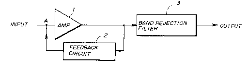
Referring to FIG.2, an amplifier circuit has a
high-gain amplifier 1, a feedback circuit 2 and a band
rejection filter tBRF) 3. The feedback circuit 2 is
connected between the input terminal and output terminal
of the high-gain amplifier 1. The band rejection filter
3 has an input terminal connected to the output terminal
of the high-gain amplifier 1, and an output terminal at
which an amplified signal is obtained.
The feedback circuit 2 feeds back an unstable
output obtained at the output terminal of the high-gain
amplifier 1 to the input terminal thereof, and causes
the high-gain amplifier 1 to oscillate at a
2S predetermined frequency (inherent oscillation
frequency). The unstable output obtained at the output
terminal of the high-gain amplifier 1 results from a
noise appiied to the high-gain amplifier 1 when no input
signal is applied thereto, and has a level equal to or
less than a predetermined level of the output signal
output by the high-gain amplifier 1. It is not required
that the above unstable output signal be amplified. The
band rejection filter 3 eliminates an oscillation output
obtained while the high-gain amplifier 1 is
oscillating.
The output signal of the high-gain amplifier 1
is partially fed back to the input terminal thereof due
.. .. .
. . .
.. .. ..
., ....................... .,.~.~ , ' . .
2 r~
-- 4 --
1 to the function of the feedback circuit 2. During the
above operation, the feedback circuit 2 functions to
cause the high-gain amplifier 1 to oscillate at the
inherent oscillation frequency thereof. However, it is
necessary to prevent the high-gain amplifier 1 from
oscillating at frequencies which are required to be
output. In other words, it is not required that the
feedback circuit 2 oscillate at frequencies of the
output signal to be output.
The high-gain amplifier 1 has an input/output
characteristic as shown in FIG.3. The input/output
characteristic curve illustrated by the solid line in
FIG.3 has a flat portion in which the output of the
high-gain amplifier 1 is substantially constant, and a
changing portion in which the output decreases
substantially linearly as the input decreases. The
high-gain amplifier 1 has a threshold output level Th
which is a boundary between a stable output range and an
unstable output range. In this unstable output range,
the output signal of the high-gain amplifier 1
fluctuates. In other words, the high-gain amplifier has
a saturated state, and has a high gain when the input
signal is small, and a low gain when the input signal is
high. The feedback circuit 2 functions to feed back
signal components having levels equal to or less than
the threshold level Th. It is not required that such
signal cGmponents be amplified.
The signal components fed back to the input
signal of the high-gain amplifier 1 ~unction as a
trigger signal which causes the high-gain amplifier 1 to
oscillate at its inherent oscillation frequency. The
osc~llation frequency is prevented from passing through
the band rejection filter 3. With the above-mentioned
arrangement, it is possible to prevent the amplifier
clrcu~t shown in FIG.2 from outputting noise components
when no input signal is applied thereto.
FIG.4 illustrates the configuration shown in
.... . . .. . .
:
. , , ' ,"" ' ' .
~ - . -.
:, ~.' '
- 5 - ~o3~S~9~
1 FIG. 2 in more detail. A hybrid circuit (HYB) 24 has an
output terminal connected to the input terminal of the
high-gain amplifier 1. The hybrid circuit 24 has a
first input terminal receiving an input signal, and a
5 second input terminal receiving a feedback signal from
the feedback circuit 2, and generates a combined signal
applied to the high-gain amplifier 1 by combining the
signals, for example, in phase with each other. A
coupler (CPL) 21 has an input terminal connected to the
output terminal of the high-gain amplifier 1, a first
output terminal connected to the input terminal of the
band rejection filter 3, and a second output terminal
connected to the input terminal of the feedback circuit
2. The coupler 21 outputs a part of the output signal
from the high-gain amplifier 1 to the feedback circuit
2.
The feedback circuit 2 has an attenuator (ATT)
22 and a variable length coaxial line 23 connected in
series. The attenuator 22 has an input terminal
connected to the second output terminal of the coupler
21, an output terminal connected to an input terminal of
the variable length coaxial line 23, and a control
terminal for receiving the aforementioned threshold
level Th. The variable length coaxial line Z3 has, in
addition to the above-mentioned input terminal, an
output terminal connected to the second input terminal
of the hybrid circuit 24. The attenuator 22 allows the
signal components equal to or less than the threshold
level Th to pass through the attenuator 22. The
inherent oscillation frequency which causes the
high-gain amplifier 1 to oscillate is determined based
on the length of the variable length coaxial line 23.
For example, the variable length coaxial line 23 is
adjusted so that the inherent oscillation frequency now
labeled ~OSC is equal to the frequency o~ the input
signal. A rejection ~requency FRJC of the band
rejection ~ilter 3 is determined so that it is equal to
..
- 6 - 2i3
1 the oscillation frequency fosc (fRJC = fosc).
When no signal is applied to the high-yain
amplifier 1 via the hybrid circuit 24, the signal
components equal to or less than the threshold level Th
pass through the attenuator 22 and the variable length
coaxial line 23, and are applied to the hybrid circuit
24. The above signal components pass through the hybrid
circuit 24, the high-gain amplifier 1 and the coupler
21, and are applied to the attenuator 22. In this way,
the signal components, that is, noise components of the
high-gain amplifier 1, are drawn into the inherent
oscillation frequency, so that the high-gain amplifier 1
is maintained in the oscillating state. Since the
rejection frequency FRJC of the band rejection filter
3 is equal to the inherent oscillation frequency fosc
no noise components are output via the band rejection
filter 3.
On the other hand, when an input signal in the
stable output range is applied to the high-gain
amplifier 1 via the hybrid circuit 24, it amplifies the
input signal without oscillating. An amplified input
signal passes through the coupler 21 and the band
rejection filter 3.
It will be noted that if the attenuator 22 is
not provided, the high-gain amplifier 1 will oscillate
in response to any input signal. For example, even if
an input signal in the stable output range is applied to
the high-gain amplifier 1, it will oscillate. For the
above reason, the attenuator 22 extracts signal
components which are equal to or less than the threshold
level Th, it not being required that they be amplified
and output. The extracted signal components function to
oscillate the high-gain amplifier 1. The setting of the
threshold level Th is carried out, taking into account
the branch ratio in the coupler 21.
FIG.5 illustrates a variation of the
configuration shown in FIG.4. In FIG.5, those parts
l which are the same as those shown in FIG.4 are given the
same reference numerals. A narrow bandpass filter (BPF)
25 is substituted for the variable length coaxial line
23. The narrow bandpass filter 25 has a bandpass range
which passes the signal components which cause the
high-gain amplifier l to oscillate.
FIG.6 illustrates another variation of the
configurations shown in FIGS.4 and 5. The variable
length coaxial line 23 shown in FIG.4 or the narrow
bandpass filter 25 shown in FIG.5 is provided between
the coupler 21 and the attenuator 22.
The present invention is not limited to the
specifically disclosed embodiments, and variations and
modifications may be made without departing from the
scope of the present invention.