Note: Descriptions are shown in the official language in which they were submitted.
-1- 2036~75
TIMB DIFFERENCE CO-P~CTION CIRCUIT FOR BRIGHTNB88 AND
CHROMINANCE 8IGNAL8
R~C~.rPOUND OF THE INVBNTION
The present invention relates to a time
difference correction circuit for brightness and
chrominance signals. As shown in Fig. 1, in playback
operation of a prior art VCR Video Cassette Recorder
system, a teletext signal or a video signal recorded on a
tape 1 is detected through a head 2 and the detected signal
passes via a pre-amplifier 3 to a frequency demodulator 4
and a 3MHz, low pass filter 5, in sequence, to detect a
brightness signal. The signal from the tape 1 also passes
through a second low pass filter 9 a main convertor 10 and
a band pass filter 11, in sequence, to detect a chrominance
signal. The detected brightness and chrominance signals
are added through an adder 6 to produce a composite video
signal 7. However, the prior VCR system has a disadvantage
in that when the signal recorded on tape 1 is played back,
a time difference between the brightness and chrominance
signals is generated which causes the brightness signal to
deviate from the chrominance signal in time and therefore
the picture image is not clear at the high frequency
characteristics of a brightness signal.
8UMMARY OF THB INVENTION
In accordance with one aspect of the invention,
there is provided a time difference correction circuit for
correcting time differences between luminance and
chrominance signals derived from a detected signal from a
videotape. The circuit includes luminance signal detecting
means, chrominance signal detecting means, mixing means,
vertical synchronization means and timing control means.
The luminance signal detection means extracts a luminance
signal from the detected signal. The chrominance signal
detection means extracts a chrominance signal from the
deleted signal and includes a controllable delay line for
delaying the chrominance signal by a controllable amount of
D
. K ,~
2036475
time to produce a time difference corrected chrominance
signal. The mixing means mixes the luminance signal and
the time difference corrected chrominance signal to produce
a composite video output signal. The vertical
synchronization means detects a vertical synchronization
signal in the luminance signal and delays the vertical
synchronization signal to produce a delayed vertical
synchronization signal. The timing control means
determines a time difference between the luminance and
chrominance signals for each field in a horizontal
interval, in response to the delayed vertical
synchronization signal and outputs a control signal to the
controllable delay line, the control signal corresponding
to the time difference between the luminance signal and the
chrominance signal. The delay produced by the time delay
is varied to correct the time difference.
Preferably, the vertical synchronization means
includes a synchronizing divider for extracting a
synchronizing signal from the detected signal of a tape, a
vertical synchronizing divider for extracting a vertical
synchronizing signal from the synchronizing signal and a
delay element for delaying the vertical synchronizing
signal to produce a delayed vertical synchronization signal
delayed to a start point of a modulated video signal.
Preferably, the timing control means includes
switching means including a monostable-multivibrator for
generating a pulse having a predetermined pulse width in
response to the delayed vertical synchronization signal, a
comparison circuit for comparing the respective amplitudes
of the luminance signal and the time difference corrected
chrominance signal to produce a comparison output signal,
first and second switches for switching the brightness and
chrominance signals to selectively apply the signals to the
comparison circuit in response to the pulse from the
monostable-multivibrator and control signal producing means
for producing the control signal in response to the
comparison output signal.
~ ~A
--- 2036475
--3--
Preferably, the control signal producing means
includes a first diode for passing only the positive
component of the comparison signal a first integrator and
a first differentiator connected to the first diode, for
integrating and differentiating the positive component of
the comparison signal to produce first integrated and first
differentiated output signals respectively, a second diode
connected to the first differentiator for passing only the
negative component of the first differentiated output
signal, a sampler connected to the second diode, for
sampling that portion of the integrated output signal which
occurs simultaneously with the negative component of the
differentiated signal, a holder connected to the sampler
for holding a held output signal of the sampler to a start
point of the next field and means responsive to the held
output signal for producing the control signal for
controlling the delay line, including a voltage controlled
oscillator, the voltage control oscillator having an output
for producing the control signal, the control signal having
a frequency responsive to the negative component of the
held output.
Preferably, the timing control means includes a
second differentiator for differentiating the output signal
of the comparison circuit to produce a second
differentiated signal, a second holder for holding the
second differentiated output signal to a start point of the
next field to produce a held differentiated output signal
and an inverter for inverting the held output signal in
response to the held differentiated output signal to
extract the negative component of the held output signal
for controlling the voltage controlled oscillator.
Preferably, the apparatus further includes a
reset circuit including a third differentiator for
differentiating the vertical synchronizing signal to
produce a third differentiated output signal and a third
diode for passing only the positive component of the third
~4~ 2036475
differentiated output signal, the output of the third diode
acting as a reset signal operable to reset the holders.
BRIBF D~P~PTPTION OF THB DRA~ING~
In drawings which illustrate embodiments of the
invention,
Figure 1 is a block diagram of a composite video signal
producing circuit according to the prior art;
Figure 2 is a block diagram of a circuit according to a
first embodiment of a time difference correction
circuit according to the invention; and
Figures 3 - 8 are waveforms of output signals appearing at
various location in the circuit shown in
Figure 2.
DBT~TT~l; n D~P"PTPTION
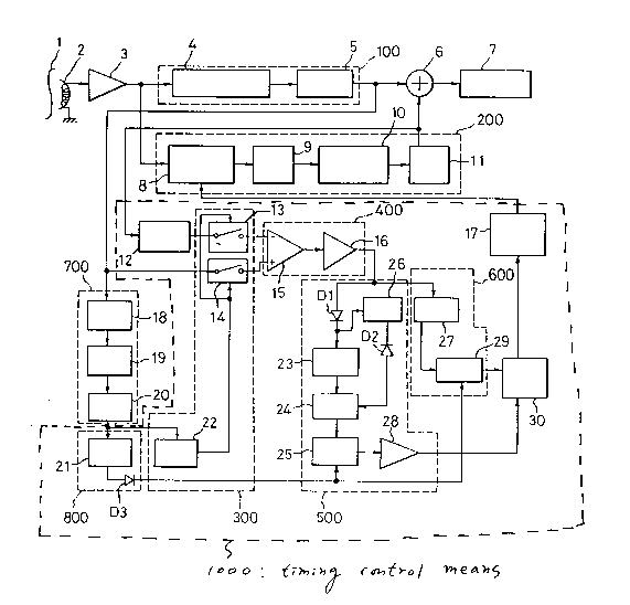
Referring to Figure 2, a VCR includes a time
difference correction circuit for correcting a time
difference between brightness and chrominance signals. The
circuit includes a head 2 for detecting a video signal from
a tape 1, and a preamplifier 3 for amplifying the detected
video signal.
The circuit further includes a luminance signal
detection circuit 100 including a frequency demodulator 4
for demodulating a frequency-modulated brightness signal
from said detected video signal and, a first 3MHz low pass
filter 5.
The circuit further includes a chrominance signal
detection circuit 200 including a CCD Charge Coupled Device
delay line element 8 for delaying an output signal of the
preamplifier 3 for 1 horizontal interval, a second low pass
filter 9 for filtering an output of the CCD delay line
element 8, a main converter 10 for converting the low-pass
filtered chrominance signal into a high-pass filtered
chrominance signal to return its original frequency, and a
band pass filter 11 for filtering an output signal of the
main converter 10.
~.,
- 2036475
--5--
An adder 6 is further provided for adding output
signals from the first low pass filter and the band pass
filter 11 to produce a composite video signal.
An envelope detector 12 circuit is further
provided for detecting the envelope of a chrominance signal
from an output signal of the band pass filter 11.
A timing control circuit 1000 is further provided
and includes a switching circuit 300 including first and
second switches 13 and 14 for switching an output of the
envelope detector 12 and an output of the low pass filter
11 to a comparison circuit ~00. The switching circuit
includes a monostable-multivibrator 22 for outputting an
on/off control signal to the switches 13 and 14. The
comparison circuit 400 further includes a comparator 15 for
comparing the outputs of the first and second switches 13
and 1~ which are applied to inverting and non-inverting
terminals, respectively thereof. The comparison circuit
further includes an amplifier 16 for amplifying the output
of the comparator 15. The output of the amplifier 16 is
applied to a difference signal generation circuit 500
including an integrator 23 and a differentiator 26 for
integrating and differentiating only the plus or positive
component of the amplified signal of the comparison
circuit 400.
The timing control circuit further includes a
sampler 24 for sampling only that portion of the integrated
signal which is associated with the minus or negative
component of the differentiated signal, a holder 25 for
holding the output of the sampler 24 before the next field
interval in which a reset signal is applied, and an
amplifier 28 for amplifying an output signal of the holder
25 by a predetermined amplification factor.
The timing control circuit further includes a
difference signal detection circuit 600 including a
differentiator 27 for differentiating the output signal of
the comparison circuit 400, and a holder 29 for holding the
-6- 2036475
output of the differentiator 27 before the next field
interval in which a reset signal is applied.
The timing control circuit further includes a
vertical synchronizing signal generation circuit 700
including a synchronizing divider 18 for dividing a
synchronizing signal from an output signal of the low pass
filer 5, a vertical synchronizing divider 19 for dividing
out a vertical synchronizing signal from the synchronizing
signal and a delay 20 for delaying the divided vertical
synchronizing signal to a start point of the modulated
video signal.
The timing control circuit further includes a
reset circuit 800 including a differentiator 21 for
differentiating the delayed signal from the delay 20 and a
lS diode D3 for passing only the plus or positive portion of
the output signal of the differentiator 21 to holders 25
and 29 as a reset signal.
OPERATION
The operation of the invention will now be
described in detail with reference to Fig. 2 through
Fig. 8.
During playback operation of the VCR, the signal
recorded on tape 1, such as a teletext signal or a video
signal, is detected by the head 2 which produces an output
signal as shown in Fig. 3A. The detected signal is
amplified by the preamplifier 3 by a predetermined
amplification factor. The amplified signal is then
demodulated in the frequency demodulator 4 and filtered
through the 3MHz low pass filter 5, the output of which is
applied to the adder 6 as a brightness signal as shown in
Fig. 3B. The amplified signal from preamplifier 3 is also
supplied to the CCD delay line element 8 of the chrominance
signal detection circuit 200 which delays the signal by 1
horizontal interval lH. High-band noise generated in the
CCD delay line element 8 is removed by the low pass filter
9 and the main converter 10 converts the low-pass filtered
- 2036475
--7--
chrominance signal into a high-pass filtered chrominance
signal to return its original frequency. The resulting
output signal is applied to the band pass filter 11 which
removes low and high frequency noise, generated in the main
converter 10, to produce a chrominance signal as shown in
Fig. 3C. This chrominance signal is applied to the adder
6 and to the envelope detector 12.
The adder 6 adds the brightness signal and the
chrominance signal to produce a composite video signal 7 as
shown in Fig. 3E.
The remainder of the circuit acts to increase or
decrease the time delay provided by the CCD delay element
8 to the chrominance signal to remove the time difference
between brightness and chrominance signals. The principle
of operation to remove the time difference between
brightness and chrominance signals is described as follows:
The output of the 3MHz low pass filter 5 is
applied to the switch 1~ of the switching means 300 and to
the synchronizing divider 18 of the vertical synchronizing
signal generation circuit 700, respectively. The
synchronizing divider 18 divides the brightness signal seen
at Fig. 3B and produces a synchronizing signal as shown in
Fig. 3F. This synchronizing signal is applied to the
vertical synchronizing divider 19 which divides the
synchronizing signal to produce a vertical synchronizing
signal as shown in Fig. 3G. This vertical synchronizing
signal is applied to the delay circuit 20 which delays it
to a start point of the video signal which is a modulated
2OT signal as shown in Fig. 3H and included in the vertical
blanking interval.
The delayed vertical synchronizing signal is
applied to the differentiator 21 of the reset circuit 800
and to the monostable-multivibrator 22 of the switching
circuit 300. The signal produced by the differentiator
acts as a reset signal and is applied to the holders 25 and
29. The output signal of the monostable-multivibrator 22
has a pulse width corresponding to lH interval as shown in
2036475
--8--
Fig. 3I and is applied to switches 13 and 1~ as a control
signal.
When the control signal from the monostable-
multivibrator 22 is active, the chrominance signal as shown
in Fig. 3D through the envelope detector 12 and a
brightness signal as shown in Fig. 3B are applied to the
comparison circuit 400. Thus, only brightness and
chrominance signals as shown in Fig. 3B and C,
corresponding to the modulated 20T signal are applied to
the inverting and non-inverting terminals of the comparator
15 of the comparison circuit 400 through switches 13 and
14, respectively.
The comparator 15 compares the level of the
brightness signal as shown in Fig. 3B with that of the
chrominance signal as shown in Fig. 3C and outputs a signal
corresponding to the difference between them. As shown in
Fig. 4, when there is no time difference between the
brightness and chrominance signals as shown in Fig. 4B and
C, of a composite video signal as shown in Fig. 4A, there
is no output of the comparator 15 as shown in Fig. 4D so
that the output signal of the amplifier 16 is negligible as
shown in Fig. 4E.
However, as shown in Fig. 5, when a brightness
signal as shown in Fig. 5A appears in advance of the
chrominance signal as shown in Fig. 5B, the comparator 15
outputs a signal as shown in Fig. 5C so that the amplifier
16 outputs a rectangular wave signal as shown in Fig. 5D.
On the other hand, as shown in Fig. 6, when a chrominance
signal as shown in Fig. 6B appears in advance of the
brightness signal as shown in Fig. 6A, the comparator 15
outputs a signal as shown in Fig. 6C so that the amplifier
16 outputs a rectangular wave signal as shown in Fig. 6D.
The output signal of the comparator 15 is
amplified through the amplifier 16 so that the rectangular
wave signal is applied to the integrator 23 and to the
differentiator 27. Only the plus or positive portion of
the signal is passed through diode Dl as shown in Fig. 3J
`~ ~036~75
g
and is integrated in the integrator 23 as shown in Fig. 3K.
The integrated signal is applied to the sampler 2~. At the
same time, the plus or positive component of the
rectangular wave signal is differentiated by the
differentiator 26 as shown in Fig. 3L and only the minus or
negative component of the differentiated signal is passed
through diode D2 and is applied to the sampler 2~.
Therefore, the sampler 24 samples only that portion of the
integrated signal which is associated with the
differentiated signal. The sampled signal is applied to
the holder 25 to hold its level for 1 field that is, to the
start point of the next field and the output of the holder
25 is amplified by the amplifier 28 by a predetermined
amplification factor and then applied to the inverter 30.
On the other hand, the differentiator 27
differentiates the rectangular wave from the amplifier 16
as shown in Fig. 5D and Fig. 6D and the holder 29 holds the
differentiated signal before the reset signal is applied
from the reset circuit 800. When a brightness signal
appears in advance of the chrominance signal, as shown in
Fig. 7B, the differentiator 27 differentiates the output
signal of the comparison circuit 400 as shown in Fig. 7A.
When a chrominance signal appears in advance of the
brightness signal, as shown in Fig. 7D, it differentiates
the output signal of the comparison circuit 400 as shown in
Fig. 7C. The holder 29 holds the output of the
differentiator as shown in Fig. 7B or D for 1 field
interval, that is, before the reset signal is applied.
When the vertical synchronizing signal generation
circuit 700 outputs to the reset circuit 800 a pulse as
shown in Fig. 8A, corresponding to the vertical
synchronizing signal, the differentiator 21 differentiates
the pulse as shown in Fig. 8B and the minus or negative
component of the differentiated signal is removed through
diode D3 so that only the plus or positive component is
outputted as shown in Fig. 8C. The plus or positive
portion of the differentiated signal is applied to holders
-lO- 2036475
25 and 29 as a reset signal at the end of 1 field interval.
The output of the holder 29 is applied to the inverter 30
as a control signal so that when the plus or positive
portion of the differentiated signal is applied it is
disabled, whereas when the minus or negative component is
applied, it inverts the signal from the difference signal
generation circuit 500.
The output signal of the inverter 30 is applied
to the voltage controlled oscillator 17 as a control signal
so that when there is no input signal, it oscillates
normally, but when there is an input signal, it increases
or decreases the oscillating frequency by an amount
corresponding to the level and polarity of the input signal
and produces an output control signal to control the
clocking of the CCD delay line element 8. The CCD delay
line element 8 delays the output of the amplifier 3 to
advance or retard the delay provided to the amplifier
signal. When the oscillating frequency increases, it
decreases the delay and when it decreases, it increases the
delay. Accordingly, a nominal lH delay is increased or
decreased so that the difference between brightness and
chrominance signals is corrected.
As above-stated, in the present invention, the
time difference between brightness and chrominance signals
is corrected so that degradation of picture quality is
prevented. This allows picture quality to be maintained,
even during playback of successively recorded video
signals.
While specific embodiments of the invention have
been described and illustrated, such embodiments should be
considered illustrative of the invention only and not as
limiting the invention as construed in accordance with the
accompanying claims.
~'