Note: Descriptions are shown in the official language in which they were submitted.
CA 02036595 1999-07-20
SAMPLIPJG RATE CONVERTER FOR SIGNALS HAVING A
NON-INTEGER SAMPLING RATIO
BACKGROUND OF THE INVENTION
This present invention relates to a sampling rate
converter, and is suitably applied to a~case where a
sampling freque.ncy~of component digital video signals
based on D-I(625/5.0) format Is converted to a sampling
frequency corresponding. to composite digital video
signals based on D-2 format, for example.
Heretofore, there used to be a sampling rate
converter which is constituted by a digital filter for
converting digital signals, which are obtained by
sampling analog signals at a predetermined frequency,
to an arbitrary sampling frequency.
Such a sampling rate converter is constituted by a
high order oversampling filter to strictly observe the
NYquist frequen~~y as a conversion characteristic of the
transmission syF;tem.
In FIGS. IA-ID, roughly illustrated is an
operation of a sampling rate converter constructed by
an oversampling filter having for example. In such an
oversampling filter, input digital signals (indicated
bY character in FIG. LA) are inputted to the
1
oversampling filter, the input digital signals being
provided by sampling imaginary analog signals SVT as
shown in FIG. lA at a first sampling frequency f1 (FIG.
1B).
Subsequently, the oversampling filter oversamples
input digital signals at a frequency fll 11 #imes
larger as shown in FIG. 1C as ~rell as resamples them at
a second sarinpling frequency f2 (FIG. 1D)to obtain
output digital signals which have values indicated by
characters p in FIQ. 1A and $re mate converted into
frequency f,2.
When a sampling frequency of oomponent digital
video signals based on D-1(625/50), format in digital
video tape recorder (L1VTR) is converted ,into a sampling
frequency corresponding to PAL composite digital video
signals based on the D-2(PAL) format; it is not
possible to dir'eotly convert sampling frequency between
digital video signals since the sampling frequency is '
rate converted from a frequency 13.5 Mliz to a frequency
17.734475 MHz. It is thus necessary to build an
oversampling filter having approximately a length ~f an
order of about 16500.
Also in the converse case where a sampling
frequency of PAL composite digital video signals is
2
~~~'J~~
converted into a sampling frequency corresponding to
B25/60 component digital video signals, it is necessary
to build an oversampling filter in the same circuit
scale as the above described case since the sampling
frequency is rate oonverted from a frequency 17.?34476
MHz to a frequency 13.5 MHz. It is thus inevitable
that the overall circuit soale becomes complicated and
large sized.
To solve such a problem, a sampling rate converter
has been proposed in which a oversampling filter
reduced the circuit scale is built so that on the basis
of the relationship of sampling frequencies 13.5 MHz
and 1:734495 MHz between 826/50 component digital
vidoo signals and PAL composite digital vidoo signals,
a oversampiing trequenoy is set, and filter
coefficients input changeably to one multiplier
corresponding to a magnification of the oversampling to
v~reight tho sampling data.
FIG. 2 illustrates a basic construct9on of a
sampling rate converter 1 having changeable
coefficient. In a case where in a sampling rate
converter 1 as shown in FIG. 2, a sampling frequency of
625/50 component digital video signals is converted
into a sampling frequency corresponding to PAL
3
N~~~~~~~r~
s
composite digital video signals, for example, 625/54
component digital video signais SINDl and output clock
signals CKDy corresponding to the sampling frequency
thereof are inputted to the timing adjusting circuit 2.
This timing adjusti~ag circuit 2 outputs data of
the 82b/50 component digital video signals SpNDl
inputted at the rate of the clock signal CKDf at the
#iming of the rate oP the clock signal CKD2 so as to
exchange the cL.oek as well as control the timing of the
data transference described below.
In addition to this, frame pulses Pp,Dl
corresponding to one frame of 625/50 component digital
video,signals slND1 are inputted to reset terminals of
a phase locked Loop (PLL) circuit 3 and a counter 4.
The output of PLL circuit 3 is feedbacked through
a frequency divider 6 with a ,dividing ratio
1/709379) correspondingto the number of samples of
otaa frame (_ 709379) of PAL composite digital vidao
Signals;
This enables the PLL circuit 3 to correctly
synchronize with frame pulses PrDf of 625/50 component
digital video signals, and the I'LL circuit 3 generates
output clock signals CKD2 corresponding to the sampling
frequency of the PAL composite digital video signals
4
41 ~ ~u t
and supplies them to a count input terminal of a
counter 4, the timing adjusting circuit 2 and an
oversampling filter 6.
The counter 4 is reset according to frame pulses
PFD1' and counts output clock signals CIfD2' inputted
from the PLL cirouit 3, every frame. Consequently,
count data DCNT K'hich is zero to 709373 is sequentially
sent'to a,coeffioient address control circuit T.
The coefficient address control circuit 7
generates coefficient address data DCOE according to
the oount data DCNT to read coefficients COEF'
COEFE, .., from coefficient generating circuits 9A,
98, . whioh are R0M (read only memories),. the
aoaffloiants COEFA' COEFB' ~~~ baing to fad to
multipliers BA, BB, .,. which are weighfiing means of
the oversampiing filter & of which part is illustrated
in FIC3: 5.
The relationship between coetficients COEFA'
C~EFB, . . supplied to the rziultipliers SA, BR, .,, and
tlhe ooeffieient address data DCOE is illustrated
schematically ire FIG. 4. In FIG. 4, a longitudinal°
axis represents the ooeffieient C~EF and lateral axis
represents the coefficient address data DCOE. The
lateral axis also be able to see as a time axis. "N"
S
is the order of the oversampling filter and is derived
from the characteristic of the oversampling filter
required. An impulse response characteristic of the
oversampling filter is formed by N groups of the
coefficient C~~F. It is got that a practical impulse
response characteristic is illustrated in FIG. 4, it is
illustrated schematically.
°'Ie'T" represents numbers of division between
sarnpl ing points to tha input signal BINZ)1, that is~ a
resolution capability, by which the oversampling
frequenoy is decided, The groups of coefficient are
divided b.y M groups so as to store them in the
ooefficient generating circuits 9A; BB, .., the number
of which are M/N. The address a0.., an, b~... bn are
apointed with a coefficient address data DCOE generated
at the rata of the clock signal CKD2 in the coefficient
address control circuit so that the groups of
ooeffioient cOEF stored is read out.
The relationship between the count data DC~T and
the address of the coefficient generating circuits 9A,
9B; ... apointed with the coefficient address data °bCOE
is illustrated in FIG. 5. In the case illustrated in
FIG. 6, the oversampling filter is constructed with
orders N = 4554, M = 506. The coefficients which form
6
the impulse response characteristic of the oversampling
filter are stored in sequence at the addresses ffrom a0,
b0, ~~~ i0 to x605' b505. In the under portion of FIG.
5, the coefficient addresses DCO~ which are generated
at the timings of each of the count data DC~~, are
illustrated. In FIG. 6, with the count data DG~~,
exchanged in sequence n, n+1, n+2, .., at the rate of
clock signal CKD2, the coefficient address data DGGE is
generated so that the addresses a0 - a505' b0 b6'05'
00 °606' ~~~ are apointed in sequence (a0, b0,
...1~(a388' b388' 0388' ~..1' (x288' b28B'
0288' ...]. ....
The apointment of the address in each of the
0oeffioiant generating circuit is performed on the
basis of the relationship between the sampling period
of 825160 component digital video signal and the
sampling pet~iod of PAL composite digital video signal
so as to shift by 388 addresses cyclS'cly among
addresses 0 - 606 as following equation.
13.5
608 * - 388 ... (1)
17.7
7
~~~~~~i
The coefficients CpEFA CpEFI generated in the
coefficient generating circuit 9A - 8I are rnultipiied
by the output data in the multiplier. When the count .
data DCNT becomes predetermined values, for instance
DCNT becoming DCNT = n + 1 in FIG. 5, it is necessary
to multiply a coefficient corresponding to DCNT = n + 1
by the same data as the flip-flop output data
multiplied at the timing DCNT = n. In this case, the
coefficient address control circuit 9 generates a shift
control signal DEFT to stop the data transference in
the flip-flop circuits l0A - l0I(this means having
shifted one block data) so as to be able to multiply in
the multiplier using the same flip--fiop output data.
The shift control signal DAFT also is provided to
the timing adjusting circuit. This result in stopping
the exchange of the clock according to stopping the
operation of the data transference from the flip--flop
circuits l0A - 10I; whereas the exchange of the clock
continues in the timing adjusting circuit 2.
As described above, the timing adjusting circuit 2
adjusts timing of inputted 625/50 component digital°
video signals ~IND1 to send to the oversampling filter
6 according to the output clock signals CKD1, the
output clock signals CKD2, and the shift control data
8
DSFT'
The oversarnpling ffilter 8 performs oversampling by
multiplying the 825/60 component digital video signals
SINDi thus inputted by coefficients C~EFA' COEFB' " '
according to the shift control data DSFT and the
coefficient address data DCCE, and provides outputs
aocording to output clock signals CKD2. In this
manner, output digital video signals SpUTD2 are
obtained by canverting the sampling frequency of 625150
component digital video signals to a sampling frequency
corresponding to PAL composite digital video signals.
It is to be noted that in the oversampling filter
8 input digital signals SIN are fed to a series circuit
flip-flops 10A, lOB, ... having a delay according to
outpu# olock signals CKD2. Delayed digital signals
sentout from each of the flip-flops IOA, tOB, .., are
inputted to suhsequent flip-flops 1OB, ... and to
corresponding multipliers $A, SB,....
Predetermined ooefficients CQE~;A, COEFB' "
described above are inputted from the coefficient
generating circuits OA, OB, ... to respective
multipliers 8A, SB, ..., and consequently, the delayed
digital signals are multiplied by respective
coefficients CpEP,A' COEFB' " "
9
2~~~~~
Results of the multiplication are inputted to each
of adders llA, 118, .., for providing a total, and the
result of this addition is sent out as output digital
video signals BOUT'
The sampling rate converter 1 with such a
construction has a large scale circuit configuration in
which the counter 4 counts a value 0 to 709878. Also,
the coefficient address control circuit 7 inevitably
has a large scale circuit configuration for processing
oount data DCNT from the counter 4. Consequently,
there is a problem in that the sampling rate converter
1 beoorues large sized.
SUMMARY OF THE INVENTION
In view of the foregoing,'an object of this
Invention is to provide a sampling rate converter which
is oapa:ble of oonverting a samgling frequency of
digital signals sampled at a first sampling frequency
to a second sampling frequency with a simple
construction.
In accordance with a first aspect of this
invention, there is provided a sampling rate converter
20 for converting a sampling frequency of digital
signals sampled at a first sampling frequency to a
second sampling frequency, the sampling rate converter
including an oversampling filter 8 having coefficient
generation means 9A., 9B for generating coefficients.
CoEF~, CCEFB to be provided to weighting means 8~., 8B
according to coefficient addresses DCCE1, there are
according to the present invention provided for solving
such a problem: counting means 21 for counting output
clocks CKD2 in a cyclic fashion; correction value
generation means 22, 28 for generating a coefficient
correction value DHC in accordance with a number of
counts of a maximum value CDC and the periodicity of
the first and second sampling frequencies, the number
of counts of the maximum value being obtained by
counting maximum value information 5C~ sent from the
counter means 21 every time the counter means counts to
the maximum ve~lue; and coefficient address generation
moans 23, 2d, 2? for generating the coefficient
addresses DCpEl in acoordanco with the counted value
DCIQT1; inputted iroxn the countor means 21, and the
coefficient correction value DDC inputted from the
correction value generation means 22, 26.
In thus construction, output clocks CICD2
corresponding to the second sampling frequency are
counted in the cyclic fashion from the initial value to
11
~t3~~~f~w~
the maximum value based on periodicity of the first and
second sampling frequencies. Coefficient addresses
DCOE1 are generated in ~.ceordanea to the resulting
count value DCNT1 and the coefficient correction value
DHC in accordance with the number of counts of the
maximum value CHC and the periodicity of the first and
second sampling frequencies, the number of the maximum
value counts being the number of times of counting to a
maximum value. The sampling frequency of digital
signals sampled at the first sampling frequency is thus
converted to the second sampling frequenoy with a
simple oonstruction of counting from the initial value
to the maximum value.
The nature, principle and utility of the invention
will become more apparent from the following detailed
description when read in conjunction with the
accompanying drawings in which like parts are
designated by like reterence numerals or charaoters.
BRLEF DESCRIPTION OF THE D12AWINGS
In the accompanying drawings: °
FIG. l is a timing chart illustrating the
oversampling operation;
FIG. 2 is a block diagram showing the conventional
12
s -
sampling rate converter;
FIG. 3 is a block diagram showing part of the
oversampling filter;
FIG. 4 is a graph showing. the relationship between
the coefficient and the coefficient address data;
FIG. 6 is a schematic diagram showing the
relationship between the count data DENT and the
coefficient address data DGOE;
FIG. 8 is a block diagram showing one embodiment
of the sampling rate converter according to this
invention; and
FIG. ? is a schematic diagram showing the shift of
th.e coefficient address data with the correction.
DETAILED DESCRIPTION OF THE INVENTION
Prefsrred embodiments of this invention will be
described with reference to the accompanying drawings:
(1) Principle of the Embodiment
In a sampling rate converter of this embodiment,
the sampling frequency ef component digital video
signals based on the D-1(825/64) format in digital °
video tape recorder (DVTB) is converted to a sarupling
frequency corresponding to PAL composite digital video
signals based on the D-2(P1~L) format.
1~
In practice, the sampling frequency of component
digital video signals based on the D-1(82b/50) format
is defined to 13.5 MHz, and the number of samples per a
line of digital video signals is hence 864. The total
number of samples of one frame amounts to 540,000.
The sampling frequency of PAL composite digital
video signals based on the D-2(PAL) format is 17.734475
MHz which is four times the sub-carrier frequency f~C
calculated based on the following equation, provided
the horizontal frequency fh is 15.825 KHz:
1 50
fSC ~ (284 - )fh +
4 2
_ 4.43361875 (MHz) . (2)
Accordingly, the number of samples par a line of
digital video signals is 1135:0064, and the total
number of samples of one frarae is 70937$.
As described, the ratio in number of samples per a
line of the 625/50 component digital video signals'over
the PAL composite digital video signals is
804:1135.0084, and it is understood that the ratio does
not have an appropriate integer relationship.
When a sampling frequency is converted using an
oversampling filter with a sufficient length, the
oversampling filter may be of_ a coefficient switch type
construction. In this case, the combination of
coefficients given to the oversampling filter must
correspond to the phase between the pre-conversion
sampling frequency and the pst-conversion sampling
frequency.
As already described, there is no relatively small
integer ratio between the pre-conversion sampling
frequency and the post--conversion sampling frequency,
and if is hence necessary to count sampling points per
a frame so as to generate a coefficient corresponding
to the count value.
The sampling cycle of the 625/50 camponent digital
video signals is computed from the following equation:
1
- 74.074074 (nsec) ... {3)
1 S . 5 ( TviH z ) '
~'he sampling cycle of the FAL composite digital video
signals is computed from the following equation:
1
- 56.58734724 (nsee)
X7.734495 (MHz)
... (4)
By detecting the time difference between the
sampling point corresponding to the sampling frequency
of 625150 component digital video signals and the
sampling point corresponding to the sampling frequency
of PAL composite digital video signals from the top of
a frame, the number of samples of the 625?50 component
digital video signals becomes a value given as equation
below at a time point of 423 samples of PAL composite
digital video signals when counter! from the top of the
frame:
56.38734724 (nseC) ~x 423
_ 321.9999464
?4.074074 (nsee)
... (5) °
the sampling points of both become closer in timing.
Sampling points of both which correspond to the
16
sampling cycles of 626/b0 component digital video
signals and FAL composite digital video signals.become
closer every multiple of 423 sample points at the
sampling cycle of PAL composite digital video signals.
In this embodiment, coefficient addresses and the
data shift control are held between 423 sample points
with reference to the sampling cycle of the PAL
composite digital video signals. In this manner,
correction of time given by the equation below is .
performed every 423 sample points at tho sampling cycle
of the PAL composite digital video signals.
b6.38734724 (nsec) x 423
- 74.074074 (nsec) x 322
- 0.00386786 (,nseo) ... (g)
In phase shifting and generatibn of coefficients, the
correction above described is carried out by providing
a counter which counts sampling within a small range
between 423 sample poin s: This enables the ss:mpling
frequency to be converted at a high accuracy with ~e
simple construction.
(2) Sampling hate Converter of the Embodiment
17
~~~~~~~5
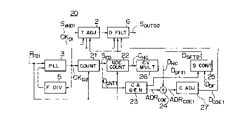
In FIG. B, in which corresponding parts of FIG. 2
are given the same reference numerals, 20 generally
designates a sampling rate convErter which converts a
sampling frequency of B25/50 component digital video
signals to a sampling frequency according to PAL
composite digital video signals, for example. In this
embodiment, frame pulses P~,~1 which correspond to every
one Prame of 625/50 component digital vidoo signals
SINI31 are inputted to a PLL circuit S, a reset input
terminal of a oounter 21, and a reset terminal of a
number-of-corrections counter 22.
The counter 21 is adopted in place of the
conventional counter 4 which counts to ?09378 and is
designed to aount output clook signals CKD2 in a cyclic
manner from zero to 922 on the ba is of the principle
stated in connection with the' equations (3) to (8)
daring one frame of 025/60 component digital video'
signals SINT1],.
The uountar 21 thus oounts output olock signals
CICDZ during one frame. The counter 21 sends resulting
count data DGNTI which is from zero to 422 to a
coefficient address generation circuit 23, and also
sends a carry signal SCE, which is' generated every time
the counted value exceeds 422, to the correction
18
.~ ~.~ i3 '~ R.
frequency counter 22.
The coefficient address generation circuit 23
generates an coefficient address ADRCCE and shift data
D~F~,1(this signal has, the same function as the function
of shift control signal DEFT' 1~e, data transference
function and clock exchange stopping function) in
response to the inputted count data DC~TZ, and sends
them to an adder 24 and a shift control circuit 26,
respectively.
During one frame, the number-of-corrections
counter 22 counts inputted carry signals SCO to
generate number-of-corrections data CRC, which is sent
to a corrected value multiplier 2B.
The corrected value multiplier 26 calculates
number-of-corrections data CDC by multiplying the
correction value (= 0.00396796 (nsee)) described in
connection with the equation (6) with the number-of-
corrections data CHC, the corrected value data DRC
corresponding to correction of the coefficient address
ADRCOE based on the number of corrections. The
corrected value data DHC is fed to the adder 24.
The adder 24 adds the coefficient address ADRCOE
and the corrected value data DDC to produce a corrected
coefficient address ADR , which is
COE1 Provided to a
19
coefficient adjusting circuit 2?.
On the basis of the corrected coefficient address
ADyCOEi° this coefficient adjusting circuit 27
generates coefficient address data DCOE1 and sends it
coefficient generating circuits 9A, 9B, ... of the
oversampling titter 6.
Ivioreover the coefficient adjusting circuit 27
detects whether or not the coefficient address ADRCOE1
is in overflow comparing with the coefficient address
ADRCOE before correction so as to send the resultant to
ttae shift control circuit 25 as a overflow data DOF.
Hence, the overflow means the fact following. In FIG.
7, when the count data DCNT is DCNT ° n the address
x137 is appointed as the address o! the coefficient
g~nerating circuit; subsequently when the count data
DCNT becomes DCNT - n + 1 the, address ap is appointed
b3~lmeans of correction. On the contrary, when the
counC data 11C~~, beepmes DCNT ~ n ~' 1~ the address asOb
is'appointed unless the address moves by means of
correction.
The overflow means that the address exceeds a'
round where the accesses of a round is from a~ to ab05'
if thus overflow generates, it is needs to process as
follow. That is, if there is an address relationship
as FIG. 7, the output data of the flip-flop circuit l0A
to be multiplied by the coefficient having the address
a0 needa to data transfer afresh by one Block, unless'
it is such data as stopped transfering the data which
is multiplied by the coefficient. The operation "stop
of data transference" and "stop of clock exchange"
described above are put a stop to.
The shift control circuit 25 detects whether or
not there is need "stop of data transference" and "stop
of clock exchange" And sands the resultant signals
as shift control signals SgFT2 to the timing adjusting
circuit 2 and the oversampling filter B.
Consequently, the timing adjusting circuit 2
controls timing of sending inputted &26/50 component
digital video signals SfNDl to the oversampling filter
6 according to the output clock signals CKD1, the
output olack signais C%D2, and the shift control data
DSFT2'
The oversampling filter 6 performs oversampling by
multiplying the 626/50 component digital video signals
SIND1 thus inputted by coefficients C~EFA, COEFB' '~"
according to the shift control data DgFT2 and the
coefficient address data DCOEI, and conducts resampling
according to the output clock signals CK~2 and outputs
21
'~~~~'~~~
the resultant data. In this manner, output digital
video signals spUTD2 "'hick are produced by converting
the sampling frequency of 825/50 component digital
video signals to the sampling frequency of PAL
composite digital videa signals are obtained.
The oversampling filter 6 has coefficients equal
in number to 606 times oversampling filter, and hence
has a resolution,of 1/505. In fact, the correction (_
0.00396;795 (nsec)) stated about the equation (6) i~s
0.027068 times as large as the resolution. This value
means that correction is carried out 45 times (that is,
0.178 (nseo)) at the trailing end of one frame. To do
this, the counter 21 and the number-of-corrections
oaunter 22 are controlled to be placed in initialized
states by resetting them every frame.
According to the foregoing construction, sampling
points are sequentially scanted in a small range of 423
sampling points; and the predetermined eorrection is
aarrie'd out every 423 sampling points. The sampling
rate converter 20 is realized which enables the counter
circuit to be built with a simple circuit construction
y,~hich counts zero to 422, and which is capable of
converting a sampling frequency of 825/50 component
digital video signals to a sampling frequency according
zz
to PAL composite digital video signals at a high
accuracy.
lyioreover, according to the foregoing construction,
the coefficient address generation circuit 2S is also
built with a simple circuit construction by
constructing the counter 21 with a simple circuit
construction which counts z~aro to 422. A sampling rate
converter is thus realized which is capable of reducing
in circuit scale to about 1/1677 of the conventional
sampling rate converter 1 (FIG. 2), resulting in a
remarkable reduction in overall scale.
Z3
~Q~~~~
(3) Other Embodiments
(3--1) In the embodiment above, a case where a sampling
frequency of $25150 component digital video signals is
converted to a sampling frequency according to PAL
composite digital video signals is stated but this
invention is not limited to this. This invention is
suitably applied to a case where a sarripling frequency
of PAL composite digital video signals is converted to
a sampling frequency according to 625/50 component'
digftal video signals.
It is to be understood that in this case an effect
similar to that of the preceding embodiment will be
aohieved by adding the aorreotion (= 0.00396795 (nsec))
described about the equation (6) every 322 sampling
points of a sampling cycle of 625/50 component digital
videa-signals according to the principle of this
linven.tion stated about the equations (3) to (5).
(3-2) In the preceding embodiments, oases where a
sampling frequency of PAL composite digital video
signals or 625/50 component digital video signals is
converted to a sampling frequency according to 825/50
component digital video signals or PAL composite
digital video signals are stated, but this invention is
not restricted to these. This invention is suitably
24
applied to various cases where a sampling frequency of
digital signals is converted to a new sampling
frequency which is not in a relationship of a simple
integer ratio with the sampling frequency.
(3~3) fn the preceding embodiments, a case where a
range among every 423 sampling points of a sapnpling
cycle of h'AL composite digital video signal is counted
i~ s.tated, but this invention is not limited to this.
This invention is suitably applied to a case where a
range among every sampling points being integer times
as many as 423 is counted.
While there has been described in connection with
the preferred embodiments of the Invention, it will be
obvious to those slcilled in the art that various
ohanges and modifications ruay be made therein without
departing from he invention, and it is aimed,
therefore,, to cover in tho appended claims all such
ohanges anrl modifications as fall within the true
spirit and soop~ of the invention.