Note: Descriptions are shown in the official language in which they were submitted.
`-` 2~7~
LEAD FRAM~
BACKGROVN~ OF THE INVEN~ION
The present invention relates to a lead frame u3ed, for
example, as a component for producing a multi-co~e optical
modula.
A multi-core optical module, in which a plurali$y of
optical operation elements (laser-diodes, photo diodes, etc.)
are linked to a number of optical fibers, is used for
building an optical communication system such as an optical
local area network ~LAN).
To produce such a multi-core optical module, electronic
circuit elements are mounted on a substrate portion la of a
lead frame (Fig. 1 or 2) and optical connectors fixing
optical operation elements are connected to the substrate
portion through wires. Subsequently, the lead frame is
attached to a mold die, after which the multi-core optical
module is produced by filling the mold die with resin.
However, when the optical operation elements including
optical transmission circuits and optical receiving circuits
are mounted on the single substrate portion la of the
conventional lead fram 1 as shown in Fig. 1, signals of the
optical transmission circuits may flow into the optical
receiving circuits (cross talk) since they have a common
ground, so that erroneous operations are apt to occur.
Further, the substrate portion la has an unnecessarily large
area, so that a thermal stress ak and after the molding step
-- 1 --
:'
~ - ~ \
`- 2~0~i
may cause deterioration by cracks generated in a ~ormed resin
portion.
On the other hand, when the substrate portion la is
divided into two parts a~ in the conventional lead frame 1 as
shown in Fig. 2, each being supported by three portions to
electrically insulate the circuits, the substrate portion la
is apt ~o move before the molding step, so that wires
connecting the optical operation element to the substrate
portion la are ant to be damaged. Further, the substrate
portion la is ap~ to vibrate due to an ultrasonic applied at
the wire bonding, so that it is difficult to assure a
sufficient strength of wire bonding.
SUMM~RY OF THE INVENTION
Therefore, an object of the presen~ invention is to
provide a lead frame in which a plurality of substrate
portions are sufficiently fixed and are sufficiently
insulated from each other in a final product. `
This ob~ect is accomplished by providing a lead frame
including a frame portion, a plurality of substrate portions
on which electronic circuit elements are to be mounted, and a
support portion for supporting the plurality of substrate
portions to the frame portion, the support portion having a
plurality of separated end portions connected to the
respective substrate portions at the position where a molded
resin member is covered, and at least two of the plurality of
end portions being combined into one body to b~ connected to
. ~, . -. .
- . . ..
-'''' ~' '' ',
,'' ~'',' ~'
.
~, .
2 ~
the frame portion at the posi~ion where the molded resin
member is not covered.
According to the lead f rame of the present invention,
since the respective substrate portions are connected to the
support portion, the substrate portions are sufficiently
ixed to the frame portion. Further, sinoe the support
portion has the separated end portions at the position where
the molded resin member i5 covered, the plurality of
substrate portions are insulated from each other by cutting
the end portions after resin molding.
BRIEF DESCRIPTION OF THE DRAWINGS
FIGs. 1 and 2 illustrate lead frames of prior art;
FIG. 3 shows the first embodiment of a lead frame
according to the present invention; and
FIGs. 4 to 7 show lead frams according to the second,
third, fourth and fifth embodiments of the present invention,
respectively.
DETAILED DESCRIPTION OF THE INVENTION
Preferred embodiments of the present invention will be
described with reference to the accompanying drawings.
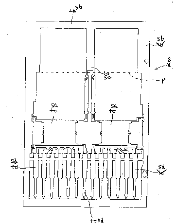
Fig. 3 shows a lead frame according to a first e~bodiment
of the present invention. In Fig. 3, a lead frame 5 includes
a support portion 5c disposed between a frame portion 5b and
substrate portions 5a r and lead pins 5d. The lead frame is
attached to a mold die at resin molding, and a resin is
~illed into a cavity of the mold die so that a package
~ 3 --
;
. . .
;
- 2~3~0~
portion is formed. A dotted line in the figure schematically
shows the package portion P ~ormed integrally by the resin
molding. The support portion Sc has two separated end
portions inside the resin package portion P so as to support
the respective substrate portions 5a and the lead pins Sd to
the fxame portion 5b. The separated end portions are
combined into one body outside the package portion P to ~e
connected to the frame portion 5b. Accordingly, the
substrate portions 5a are sufficiently fixed to the frame
portion 5b and the substrate portions are sufficiently
insulated from each other by cutting the separated end
portions after the resin molding.
When the above lead frame is used to form a multi-core
optical module, electronic circuit elements are mounted on
the substrate portions 5a and are connected to the lead pins
5d and to optical operation elements fixed to optical
connectors. Then the lead frame is subjected to the resin
molding to form the multi-core optical module.
FIG. 4 shows a second embodiment of the present
invention. The second embodiment is equivalent to the first
embodiment except that the support portion Sc has a stress
absorbing portion 5f which is a thin zigzag portian provided
in the support portion 5c.
The stress absorbing portion 5f will readily deform under
applied stress. Thus, even if the support portion 5c becomes
shorter due to the contraction of résin after resin molding,
- 4 -
: - .
. ~:
~ . . ~ , . ...
2 {~ 3 r~ 9 ~ ~;
the stress absorbing portion Sf will stretch to compensate,
relieving the frame portion Sb f rom undesired stress . Slnce
the frame portion 5b is no longer pushed, ~he lead pins 5d
are no longer forced out of the inside of the formed resin.
There is no clearance at the in~erface between the lead pins
5d and the formed resin portion, and consequently, humidity
resistance and pull-out strength of the lead pins 5d are not
diminished. Because no substantial stress is applied to the
inner portion of the lead pins, wires bonded to the lead pin
5d are safe from breaking. Further, when unnecessary
portions of the lead frame in a final product are cut off by
a stamping die, it is possible to cut the portions at an
accurate position, because ~here is no deformation of the
frame portion caused by the undesired stress.
FIG. 5 shows a third embodiment of the present invention
This embodiment is equivalent ko the second embodimet except
that stress absorbing portions lSf are disposed on a frame
portion 5b. In this embodiment, when the support portion 5c
becomes shorter due to the contraction of resin after resin
molding, the stress absorbing portions 15f will contract to
compensate, releiving the frame portion 5b from undesired
stress.
FIG. 6 shows a lead frame according to the fourth
embodiment of the present invention. This embodiment is
equivalent to the third embodiment shown in FIG. 5 except
that the separated support portion is combined into one body
... . ..
, , ;,
2~7~
at the frame portion. This embodiment has ~l~o ~he same
effects as those in the second embodiment. In this ca~é, a
resin may enter into portion ~ between the ~eparated portion8
of support portion at the molding step, so that burrs are
formed. However, this burrs can be removed at a subsequent
step.
FIG. 7 shows a lead frame according to the fifth
embodiment of the present invention. ~his embodiment is
equivalent to the second embodiment shown in FIG. 4 except
that three substrate portions 5a and two support portions 5c
are provided. This embodiment has also the same effects as
those in the former embodiments. That is, the present
invention is also applicable to a multi-core optical m~dule
having more than three cores.
It will be readily apparent to those skilled in the art
that other embodiments of the present invention may be
implemented without departing from the scope of inventive
concept expressed by the following claims.
- : , .
.
.
.. ~ . ~ .
.